Wafer Inspection Equipment Market Size and Share
Wafer Inspection Equipment Market Analysis by Mordor Intelligence
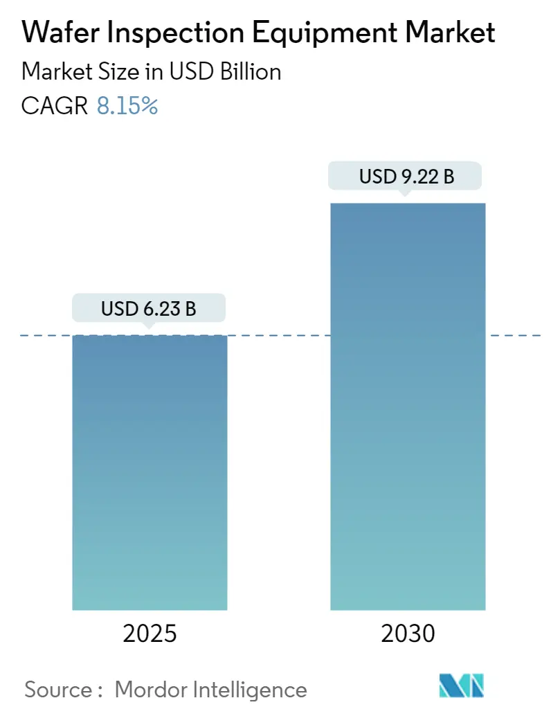
The Wafer Inspection Equipment Market size is estimated at USD 6.23 billion in 2025, and is expected to reach USD 9.22 billion by 2030, at a CAGR of 8.15% during the forecast period (2025-2030).
- The wafer inspection equipment market is a critical component of the semiconductor manufacturing industry, ensuring high-quality and defect-free wafers for downstream processing. With the growing demand for advanced electronic devices and integrated circuits, the need for precise and reliable inspection solutions has surged. Wafer inspection equipment plays a vital role in identifying defects, contaminants, and structural irregularities during various stages of semiconductor fabrication. This has become increasingly important as the industry moves toward smaller and more complex node sizes, requiring higher precision and accuracy in defect detection.
- The market is witnessing significant growth due to the rising adoption of semiconductor devices in applications such as smartphones, IoT devices, automotive electronics, and data centers. As these applications demand higher performance and efficiency, the manufacturing processes for wafers are becoming more intricate, necessitating advanced inspection technologies. Additionally, the proliferation of 5G networks and AI-driven applications has fueled the production of next-generation semiconductors, further driving the demand for wafer inspection equipment. Manufacturers are increasingly investing in innovative inspection systems that utilize advanced imaging, machine learning, and automated analysis for enhanced defect detection.
- Technological advancements are a key driver of the market, with equipment manufacturers focusing on developing more sophisticated tools capable of handling extreme ultraviolet (EUV) lithography and advanced packaging techniques. These tools are designed to address the challenges associated with inspecting wafers at nanoscale resolutions while maintaining high throughput. The integration of AI and machine learning in inspection systems is transforming defect classification, enabling more accurate and faster analyses. These innovations not only improve productivity but also help semiconductor manufacturers reduce costs by minimizing wafer rejections and process inefficiencies.
- For instance, in December 2023, Hitachi High-Tech Corporation unveiled the Hitachi Dark Field Wafer Defect Inspection System DI4600, a tool designed to inspect particles and defects on patterned wafers in semiconductor production lines. The DI4600 boasts enhanced detection capabilities,due to a dedicated server that significantly boosts data processing power for identifying particles and defects. Additionally, the system's throughput has seen a roughly 20% improvement over its predecessor, achieved by minimizing wafer transfer times and optimizing operations during inspections.
- Despite its growth, the wafer inspection equipment market faces challenges, including high equipment costs and the complexity of integrating new inspection tools into existing semiconductor fabrication lines. Additionally, the market is highly competitive, with key players focusing on R&D to maintain their technological edge. Companies are also expanding their geographical footprint to cater to the growing demand from emerging markets in Asia-Pacific, where semiconductor manufacturing is rapidly expanding. Overall, the increasing emphasis on defect-free production and technological innovation will continue to drive the market’s expansion in the coming years.
Global Wafer Inspection Equipment Market Trends and Insights
Optical Wafer Inspection Equipment Accounts For Major Share
- Optical wafer inspection equipment dominates the market due to its ability to provide high-speed, non-destructive inspection solutions critical for modern semiconductor manufacturing processes. These systems utilize advanced imaging techniques to detect surface defects, pattern misalignments, and contaminants on wafers, ensuring production quality. The growing complexity of integrated circuits and the increasing demand for high-performance chips have amplified the need for reliable inspection technologies, placing optical inspection systems at the forefront of the industry. Their capability to operate efficiently at high throughput rates makes them indispensable in large-scale production environments.
- One of the key factors contributing to the dominance of optical wafer inspection equipment is its versatility in inspecting both patterned and unpatterned wafers. Patterned wafer inspection is particularly significant as it involves identifying defects in intricate designs, which are becoming increasingly complex with shrinking node sizes. Optical systems are equipped with advanced light-based technologies that allow manufacturers to detect even the smallest deviations in wafer patterns. This precision is essential for industries such as consumer electronics, automotive, and telecommunications, where product reliability is critical.
- The adoption of optical inspection systems is further driven by advancements in imaging and automation technologies. Modern optical equipment integrates artificial intelligence (AI) and machine learning algorithms to enhance defect detection accuracy and improve classification efficiency. These advancements enable manufacturers to streamline their inspection processes, reducing downtime and increasing overall productivity. Additionally, the ability of optical systems to adapt to various wafer sizes and materials makes them a preferred choice across multiple semiconductor manufacturing applications.
- Despite the availability of alternative technologies like electron beam inspection, optical wafer inspection systems maintain their dominance due to their cost-effectiveness and ease of integration into existing production lines. While electron beam systems excel in providing detailed analyses at the nanoscale, their slower throughput and higher operational costs make them less suitable for high-volume manufacturing. Optical inspection systems, with their balance of speed, accuracy, and affordability, continue to lead the market as semiconductor manufacturers prioritize efficiency and scalability in their production processes.
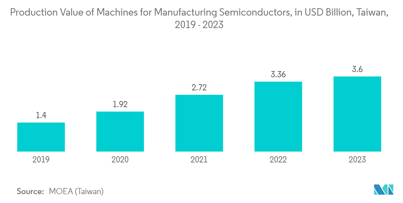
- The production value of manufacturing equipment for semiconductors in Taiwan, which amounted to over USD 3.60 billion in 2023, highlights the significant role that advanced equipment plays in the semiconductor industry. Wafer inspection equipment is a critical component of this machinery, ensuring that high-tech semiconductor products are free from defects and meet stringent quality standards. As Taiwan continues to be a global leader in semiconductor production, with companies like TSMC driving the demand for advanced manufacturing technologies, the need for sophisticated wafer inspection systems becomes even more crucial. These systems enable the detection of minute defects and irregularities on wafers, which is essential for the production of smaller, more powerful semiconductor devices. The increasing value of manufacturing equipment in Taiwan underscores the ongoing investment in state-of-the-art technologies, including wafer inspection systems, to maintain the high standards required for cutting-edge semiconductor manufacturing.
Asia Pacific Dominates The Market
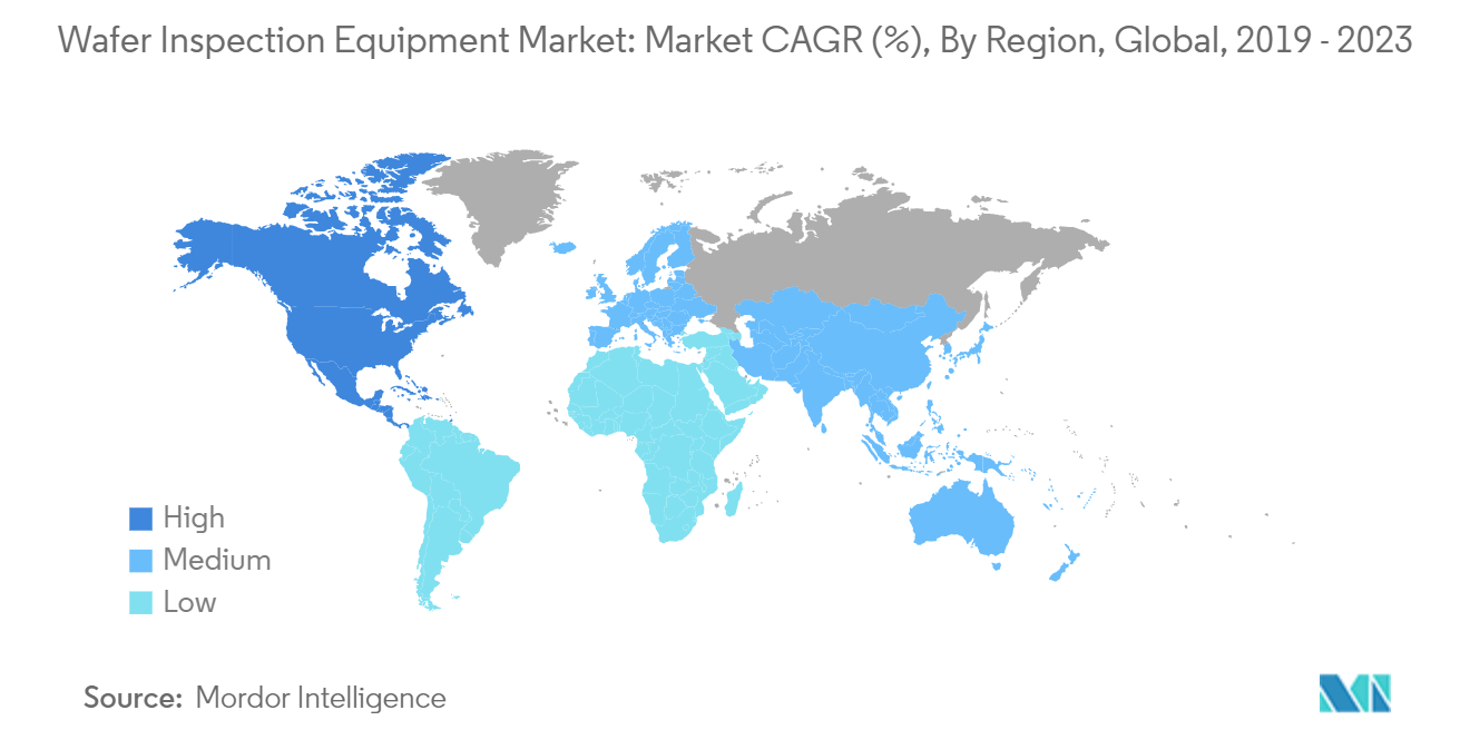
- The Asia-Pacific region dominates the wafer inspection equipment market, primarily due to its significant presence in the semiconductor manufacturing industry. Countries like Japan, South Korea, Taiwan, and China are home to some of the world’s largest semiconductor foundries, which play a crucial role in driving the demand for advanced inspection technologies. The region's focus on high-quality and efficient semiconductor production to meet the rising demand for electronic devices is a key factor contributing to the dominance of Asia-Pacific in the wafer inspection equipment market. As these countries continue to lead the global semiconductor production, the need for precise and reliable wafer inspection systems grows exponentially.
- In particular, Taiwan and South Korea are pivotal players in the semiconductor manufacturing landscape. Taiwan, with its world-leading semiconductor foundry TSMC, is one of the largest consumers of wafer inspection equipment. South Korea, home to global semiconductor giants such as Samsung Electronics and SK Hynix, also plays a major role in driving the demand for wafer inspection systems. These companies require state-of-the-art equipment to ensure the production of high-performance, defect-free wafers, especially as chip sizes shrink and the demand for more advanced semiconductor devices continues to rise.
- The rapid growth of the electronics industry, driven by the increasing adoption of consumer electronics, 5G technologies, and the expansion of the automotive sector, is also a key factor behind the Asia-Pacific region's dominance. As the demand for faster, smaller, and more efficient semiconductors continues to grow, the need for reliable and high-precision wafer inspection systems becomes even more critical. Additionally, the region’s emphasis on research and development in semiconductor technologies and manufacturing processes ensures that the demand for cutting-edge wafer inspection equipment remains high.
- Furthermore, the Asia-Pacific region benefits from the presence of numerous local and international wafer inspection equipment manufacturers. This has resulted in competitive pricing and a diverse range of inspection solutions, making it easier for semiconductor manufacturers to find systems that meet their specific needs. As the region continues to lead in semiconductor production and technological innovation, it is expected to maintain its dominant position in the global wafer inspection equipment market.
Competitive Landscape
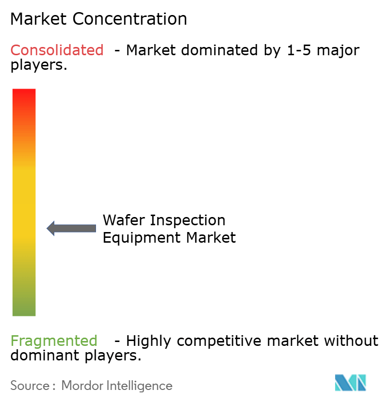
The wafer inspection equipment market is fragmented, with major players such as KLA Corporation, Applied Materials, Inc., ASML Holding N.V., Hitachi High-Tech Corporation, and Lam Research Corporation leading the industry. These companies are heavily investing in research and development to innovate and enhance their product offerings, focusing on improving defect detection accuracy, throughput, and scalability. Competition is also driven by advancements in technology, including the integration of AI and machine learning for real-time defect analysis and automated inspection processes. Strategic collaborations, acquisitions, and partnerships are common as companies seek to expand their market presence and enhance technological capabilities. Additionally, regional players are emerging in key markets such as Asia-Pacific, increasing competition and providing tailored solutions for local semiconductor manufacturers.
Wafer Inspection Equipment Industry Leaders
-
KLA Corporation
-
Applied Materials, Inc.
-
ASML Holding N.V.
-
Hitachi High-Tech Corporation
-
Lam Research Corporation
- *Disclaimer: Major Players sorted in no particular order
Recent Industry Developments
- April 2024: Onto Innovation unveiled a groundbreaking sub-surface inspection feature for its Dragonfly G3 platform, which specializes in sub-micron 2D/3D inspections and metrology. This enhancement allows for comprehensive wafer inspections, targeting critical defects that could jeopardize yields, potentially resulting in lost dies or even entire wafers breaking in later processing stages.
- March 2024: Hitachi High-Tech Corporation unveiled its latest innovation, the LS9300AD, a high-sensitivity and high-throughput wafer surface inspection system tailored for wafer manufacturers. The LS9300AD excels in identifying shallow microscopic defects, leading to decreased manufacturing costs and enhanced yields.
Global Wafer Inspection Equipment Market Report Scope
The wafer inspection equipment market refers to the industry focused on providing specialized tools and systems for detecting defects, contaminants, and irregularities in semiconductor wafers during manufacturing. These systems are essential for ensuring the quality and precision of wafers used in the production of integrated circuits and other semiconductor devices. Wafer inspection equipment includes optical, electron beam, and other advanced technologies designed to improve yield and efficiency in semiconductor production.
The Wafer Inspection Equipment Market is Segmented by type (optical inspection systems, electron beam inspection systems), wafer type (silicon wafers, compound semiconductor wafers), technology (patterned wafer inspection, unpatterned wafer inspection), application (logic and memory, led devices, mems devices, cis devices, other applications), end-use industry (semiconductor manufacturing, consumer electronics, automotive electronics, industrial, and other end-use industries), and geography (North America, Europe, Asia Pacific, Latin America, and Middle East and Africa). The market sizes and forecasts are provided in terms of value (USD) for all the above segments.
| Optical Inspection Systems |
| Electron Beam Inspection Systems |
| Silicon Wafers |
| Compound Semiconductor Wafers |
| Patterned Wafer Inspection |
| Unpatterned Wafer Inspection |
| Logic and Memory |
| LED Devices |
| MEMS Devices |
| CIS Devices |
| Other Applications |
| Semiconductor Manufacturing |
| Consumer Electronics |
| Automotive Electronics |
| Industrial |
| Other End-use Industries |
| North America |
| Europe |
| Asia |
| Australia and New Zealand |
| Latin America |
| Middle East and Africa |
| By Type | Optical Inspection Systems |
| Electron Beam Inspection Systems | |
| By Wafer Type | Silicon Wafers |
| Compound Semiconductor Wafers | |
| By Technology | Patterned Wafer Inspection |
| Unpatterned Wafer Inspection | |
| By Application | Logic and Memory |
| LED Devices | |
| MEMS Devices | |
| CIS Devices | |
| Other Applications | |
| By End-Use Industry | Semiconductor Manufacturing |
| Consumer Electronics | |
| Automotive Electronics | |
| Industrial | |
| Other End-use Industries | |
| By Geography*** | North America |
| Europe | |
| Asia | |
| Australia and New Zealand | |
| Latin America | |
| Middle East and Africa |
Key Questions Answered in the Report
How big is the Wafer Inspection Equipment Market?
The Wafer Inspection Equipment Market size is expected to reach USD 6.23 billion in 2025 and grow at a CAGR of 8.15% to reach USD 9.22 billion by 2030.
What is the current Wafer Inspection Equipment Market size?
In 2025, the Wafer Inspection Equipment Market size is expected to reach USD 6.23 billion.
Who are the key players in Wafer Inspection Equipment Market?
KLA Corporation, Applied Materials, Inc., ASML Holding N.V., Hitachi High-Tech Corporation and Lam Research Corporation are the major companies operating in the Wafer Inspection Equipment Market.
Which is the fastest growing region in Wafer Inspection Equipment Market?
North America is estimated to grow at the highest CAGR over the forecast period (2025-2030).
Which region has the biggest share in Wafer Inspection Equipment Market?
In 2025, the Europe accounts for the largest market share in Wafer Inspection Equipment Market.
What years does this Wafer Inspection Equipment Market cover, and what was the market size in 2024?
In 2024, the Wafer Inspection Equipment Market size was estimated at USD 5.72 billion. The report covers the Wafer Inspection Equipment Market historical market size for years: 2019, 2020, 2021, 2022, 2023 and 2024. The report also forecasts the Wafer Inspection Equipment Market size for years: 2025, 2026, 2027, 2028, 2029 and 2030.
Page last updated on:
Wafer Inspection Equipment Market Report
Statistics for the 2025 Wafer Inspection Equipment market share, size and revenue growth rate, created by Mordor Intelligence™ Industry Reports. Wafer Inspection Equipment analysis includes a market forecast outlook for 2025 to 2030 and historical overview. Get a sample of this industry analysis as a free report PDF download.
