
Vertical Cavity Surface Emitting Laser Market Size and Share
Market Overview
| Study Period | 2020 - 2031 |
|---|---|
| Market Size (2026) | USD 2.94 Billion |
| Market Size (2031) | USD 6.91 Billion |
| Growth Rate (2026 - 2031) | 18.64 % |
| Fastest Growing Market | Middle East |
| Largest Market | Asia Pacific |
| Market Concentration | High |
Major Players *Disclaimer: Major Players sorted in no particular order Image © Mordor Intelligence. Reuse requires attribution under CC BY 4.0. | |
Vertical Cavity Surface Emitting Laser Market Analysis by Mordor Intelligence
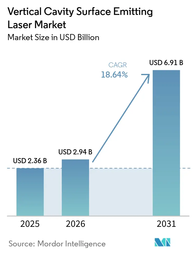
The Vertical Cavity Surface Emitting Laser Market size is expected to increase from USD 2.36 billion in 2025 to USD 2.94 billion in 2026 and reach USD 6.91 billion by 2031, growing at a CAGR of 18.64% over 2026-2031. In terms of shipment volume, the market was valued at 4.72 billion units in 2025 and is expected to grow from 6.46 billion units in 2026 to 20.18 billion units by 2031, at a CAGR of 25.60% during the forecast period (2026-2031).
Demand is shifting from legacy 3D sensing toward 200 gigabits-per-lane optical interconnects inside AI-optimized hyperscale data centers, as well as toward multi-junction arrays powering solid-state LiDAR for Level 3 autonomy. Sovereign-AI infrastructure mandates in North America and Europe favor VCSEL links over power-hungry silicon photonics for distances below 300 meters, while automotive original equipment manufacturers embed arrays with power consumption ranging from 70 watts to 400 watts to satisfy forward-collision warning rules. Epitaxial wafer suppliers are reallocating furnace capacity from gallium arsenide to indium phosphide even as yield constraints curb near-term long-wavelength supply. Shortwave-infrared devices are gaining traction due to wider eye-safety windows, and gallium nitride on silicon prototypes promise visible-light cost breakthroughs that could unlock augmented-reality and medical-diagnostic applications.
Key Report Takeaways
- By wavelength, near-infrared devices held 56.72% revenue share in 2025; shortwave-infrared is forecast to expand at a 19.37% CAGR through 2031.
- By die size, 0.06-0.4 mm² formats commanded 39.14% of the vertical cavity surface emitting laser market share in 2025, while 1.0-7.5 mm² dies are projected to grow at a 19.61% CAGR to 2031.
- By end-user industry, mobile and consumer electronics led with 47.39% revenue share in 2025; automotive is set to register the fastest 19.89% CAGR to 2031.
- By application, datacom transceivers accounted for 42.62% of the vertical cavity surface emitting laser market size in 2025, and ADAS LiDAR is advancing at a 20.56% CAGR through 2031.
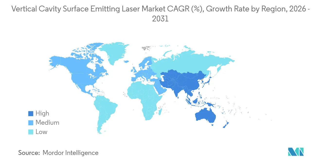
- By geography, the Asia-Pacific region dominated with a 35.77% share in 2025, whereas the Middle East is poised for the fastest 19.73% CAGR over the forecast period.
Note: Market size and forecast figures in this report are generated using Mordor Intelligence’s proprietary estimation framework, updated with the latest available data and insights as of January 2026.
Market Trends and Insights
Drivers Impact Analysis of Vertical Cavity Surface Emitting Laser Market*
| Driver | (~) % Impact on CAGR Forecast | Geographic Relevance | Impact Timeline |
|---|---|---|---|
| Surging adoption of VCSEL-based optical links in AI-optimized hyperscale data centers | +4.2% | Global, with concentration in North America and Asia-Pacific | Medium term (2-4 years) |
| Rapid integration of 3D sensing VCSEL arrays in flagship and mid-tier smartphones | +3.8% | Global, led by Asia-Pacific manufacturing hubs | Short term (≤ 2 years) |
| Transition to long-wavelength (1.3 µm) VCSELs enabling under-display biometric modules | +2.9% | Asia-Pacific and Europe, with early adoption in premium smartphone segments | Medium term (2-4 years) |
| Multi-junction VCSELs powering high-resolution solid-state LiDAR for ADAS | +3.6% | Europe, North America, and China, driven by automotive safety mandates | Long term (≥ 4 years) |
| GaN-on-Si VCSEL platforms lowering cost per emitter and expanding visible-light markets | +2.1% | Global, with manufacturing scale-up in Asia-Pacific | Medium term (2-4 years) |
| Government-backed semiconductor reshoring incentives accelerating new VCSEL fabs | +1.8% | North America and Europe, with spillover to Middle East | Long term (≥ 4 years) |
| Source: Mordor Intelligence | |||
Surging Adoption of VCSEL-Based Optical Links in AI-Optimized Hyperscale Data Centers
Hyperscale operators are upgrading from 100 gigabit to 200 gigabit lanes to satisfy east-west traffic that scales 4.2 times faster than traditional cloud workloads. Two-dimensional 64-emitter arrays now deliver 1.6 terabit throughput per module, reducing transceiver cost by 18% per gigabit and lowering power draw to 3.8 watts per terabit compared to silicon-photonics alternatives.[1] Front-panel modules are giving way to co-packaged optics that seat VCSEL dies on switch ASICs, cutting hop latency by 12 nanoseconds and driving preference for short-reach multimode links. As Microsoft Azure and other providers strive to achieve power-usage-effectiveness ratios below 1.15, the efficiency advantage of VCSELs bolsters the vertical cavity surface-emitting laser market. Capital-intensive fabs funded by CHIPS Act grants ensure local supply security and accelerate product qualification cycles.
Rapid Integration of 3D Sensing VCSEL Arrays in Flagship and Mid-Tier Smartphones
Smartphone brands have pushed 940-nanometer flood illuminators into devices priced under USD 400, doubling the addressable unit base between 2024 and 2027. New dot projectors exceed 1.2 watts peak power yet unlock faces in under 0.4 seconds under bright sunlight.[2] Compact 2.4 mm × 3.2 mm monolithic modules shave 34% board space, easing adoption in foldable hinges and wearables. Depth-map quality supports on-device AR filters and gesture navigation, while cross-industry volumes with automotive cabin cameras erode die cost by USD 0.14 annually. The use case breadth sustains double-digit growth for the vertical cavity surface-emitting laser market, even as overall smartphone shipments plateau.
Transition to Long-Wavelength 1.3 µm VCSELs Enabling Under-Display Biometric Modules
Emission at 1,300 nanometers traverses organic LED stacks with 2.8 dB less loss than 940-nanometer light, enabling secure fingerprint capture beneath 1.2-millimeter displays. Wall-plug efficiency now tops 28%, lowering battery drain to 12 milliwatts per unlock event. However, indium phosphide wafers carry 62% higher cost and yield only 74%-78%, constraining supply.[3] Equipment vendors are racing to achieve yields of over 82% by late 2026, a milestone that could open up mass-volume mid-tier smartphones to long-wavelength sensors. Until then, premium devices and medical scanners will anchor demand, ensuring a stable revenue pool for the vertical cavity surface-emitting laser market.
Multi-Junction VCSELs Powering High-Resolution Solid-State LiDAR for ADAS
Three- to five-junction stacks now deliver a peak output of 70 watts to 400 watts, enabling 200-meter pedestrian detection and meeting Euro NCAP 5-star protocols for 2026 vehicles. Automotive original equipment manufacturers prefer solid-state architectures because they reduce sensor costs from USD 1,200 to USD 380 per unit and improve the mean time between failures compared to mechanical scanners. Regulatory momentum, notably the European General Safety Regulation, creates non-discretionary demand that propels the vertical cavity surface-emitting laser market well beyond consumer electronics cycles. Thermal design remains challenging, yet breakthroughs in microchannel cooling hint at the possibility of continuous-wave operation for upcoming highway-speed autonomous vehicles.
Restraints Impact Analysis of Vertical Cavity Surface Emitting Laser Market*
| Restraint | (~) % Impact on CAGR Forecast | Geographic Relevance | Impact Timeline |
|---|---|---|---|
| Limited yield for InP-based VCSEL epitaxy constrains long-wave supply | -2.4% | Global, with acute impact in Asia-Pacific epitaxial wafer fabs | Short term (≤ 2 years) |
| Short optical reach versus silicon photonics in next-generation data center architectures | -1.8% | North America and Europe, concentrated in hyperscale data centers | Medium term (2-4 years) |
| IP concentration raises licensing costs for emerging VCSEL suppliers | -1.3% | Global, with higher barriers in North America and Europe | Long term (≥ 4 years) |
| Tight eye-safety regulations cap output power in automotive cabin applications | -1.1% | Europe and North America, driven by IEC 60825 compliance | Medium term (2-4 years) |
| Source: Mordor Intelligence | |||
Limited Yield for InP-Based VCSEL Epitaxy Constrains Long-Wave Supply
Defect densities in indium phosphide wafers remain 2.3 times higher than those in gallium arsenide, suppressing yield and keeping die costs USD 1.80 above those of 940-nanometer equivalents, a burden for price-sensitive consumer gadgets. Substrate prices average USD 420 for a 3-inch wafer, while metal-organic chemical vapor deposition reactors run at only 68% utilization, far from scale economies. Planned expansions worth USD 48 million will not reach full output until late 2027, prolonging shortages for under-display sensors and long-reach datacom links. The bottleneck temporarily hinders the otherwise robust growth of the vertical cavity surface-emitting laser market.
Short Optical Reach Versus Silicon Photonics in Next-Generation Data Centers
VCSEL multimode links top out near 300 meters at 400 gigabit speeds, whereas single-mode silicon photonics spans 2-10 kilometers. Co-packaged silicon photonics modules already consume 4.2 watts per terabit and cut hop latency by 18 nanoseconds. Hyperscalers with campus-scale fabrics must add active optical cables or hybrid architectures when VCSEL reach proves insufficient, inflating capital expenses. Precision-aligned single-mode VCSEL prototypes promise a 2-kilometer reach, but the packaging budget rises by USD 2.40 per transceiver, and volume shipments are unlikely before 2028. This technical gap siphons momentum from the vertical cavity surface-emitting laser market within ultra-large data halls.
*Our forecasts treat driver/restraint impacts as directional, not additive. The impact forecasts reflect baseline growth, mix effects, and variable interactions.
Vertical Cavity Surface Emitting Laser Market Segment Analysis
By Wavelength:
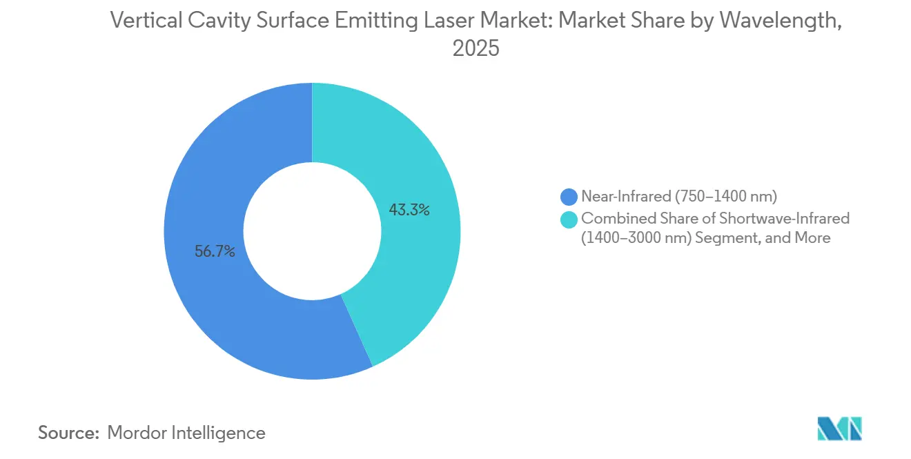
Eye-Safety Drives Shortwave-Infrared MomentumNear-infrared devices, ranging from 750 nanometers to 1,400 nanometers, controlled 56.72% of the revenue in 2025, an anchor segment for datacom transceivers and smartphone depth cameras. Shortwave-infrared emitters between 1,400 nanometers and 3,000 nanometers are expanding at a 19.37% CAGR due to looser IEC 60825 limits that allow 10 times higher optical power, a game-changer for cabin monitoring systems that must scan beyond 1.2 meters without triggering retinal-hazard warnings.
Lumentum documented 34% year-over-year growth in shortwave-infrared shipments in 2025, with automotive tier-1 suppliers integrating 1,550-nanometer arrays into head-up displays. Red wavelengths below 750 nanometers continue to fade as optical mice give way to capacitive interfaces. Bifurcated supply chains emerge: gallium arsenide fabs prioritize high-volume orders for 850 nanometer and 940 nanometer, while indium phosphide specialists chase automotive and medical margins, collectively reshaping the vertical cavity surface-emitting laser market.

By Die Size:
Large-Format Arrays Satisfy LiDAR Power BudgetsThe footprints of 0.06-0.4 mm² held a 39.14% share in 2025, as they balance thermal load with facial-recognition performance inside smartphones. To meet the 8 kW/cm² irradiance threshold required for a 200-meter LiDAR, formats ranging from 1.0 to 7.5 mm² are witnessing an impressive annual growth rate of 19.61%. This growth is driven by the increasing demand for high-performance LiDAR systems in applications such as autonomous vehicles, robotics, and advanced mapping technologies, where precise and efficient sensing capabilities are critical.
ams OSRAM now ships 3.5 mm² multi-junction arrays that reach 100-watt peaks for mid-range passenger cars. TRUMPF’s 7.2 mm² dies demonstrated 400-watt bursts, although limited to 0.8% duty cycles, prompting the implementation of microchannel cooling programs. Larger die areas yield 72% versus 88% for mid-sizes, prompting fabrication-line analytics to mitigate scrap. The scale shift highlights how ADAS adoption reconfigures revenue pools within the vertical cavity surface-emitting laser market.
By End-User Industry:
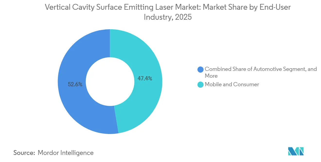
Automotive Becomes the Fastest ClimberMobile and consumer electronics accounted for 47.39% demand in 2025, fueled by 3D sensing in handsets, tablets, and XR headsets. Driven by Euro NCAP and Chinese mandates, solid-state LiDAR has become indispensable in modern automotive systems. This development has propelled automotive demand to a 19.89% CAGR, significantly outpacing consumer growth by 4.2 percentage points. The increasing emphasis on safety and regulatory compliance has further solidified the role of solid-state LiDAR as a critical component in the automotive market.
The European regulation suite lifts VCSEL dollar content per vehicle from USD 18 in 2024 to USD 64 in 2028. Lumentum reported 52% growth in automotive shipments for fiscal 2025. The telecom and medical segments remain steady, while the industrial processing sector taps into VCSEL energy density for plastic welding and selective laser sintering. Regulatory pull, rather than consumer refresh cycles, is increasingly governing the vertical cavity surface-emitting laser market's trajectory.
By Application:
ADAS LiDAR Surges Past Legacy Datacom GrowthDatacom still represents 42.62% deployment volume, anchored by 100 gigabit and 400 gigabit modules in enterprise fabrics. Multi-junction arrays, which enable centimeter-level depth resolution even at highway speeds, are driving significant growth in the ADAS LiDAR market. This technology is contributing to a robust 20.56% CAGR, highlighting its critical role in enhancing advanced driver-assistance systems.
Beyond forward-collision systems, cabins are adopting gesture control cameras to reduce driver distraction by 18%, opening incremental emitter sockets. Facial recognition, proximity sensing, and laser autofocus remain sizable but mature niches, while medical diagnostics pilots leverage 1,550-nanometer light for non-invasive glucose monitoring. The widening application spread keeps the vertical cavity surface-emitting laser market resilient, even if any single end-use stalls.
Geography Analysis
APAC Vertical Cavity Surface Emitting Laser Market
In 2025, the Asia-Pacific region commanded a dominant 35.77% share, buoyed by Taiwanese and Japanese epitaxial fabs running at an impressive 82% utilization rate. This strong performance highlights the region's pivotal role in the global semiconductor market, driven by advancements in manufacturing capabilities and robust demand for cutting-edge technologies. Meanwhile, China's CNY 28 billion investment in its compound semiconductor fund is strategically targeting self-sufficiency in 850-nanometer and 940-nanometer technologies by 2027, reflecting the country's commitment to reducing reliance on imports and strengthening its domestic semiconductor ecosystem.
North America and Europe Vertical Cavity Surface Emitting Laser Market
Coherent and Lumentum have expanded in North America, bolstered by USD 1.8 billion in CHIPS Act grants, which mitigate supply risks for hyperscalers by ensuring a more stable and secure supply chain. This funding supports the development of advanced photonics technologies critical for hyperscale data centers. Meanwhile, Europe, centered in Germany's photonics belt, benefits from its closeness to automotive tier-1 plants, which not only reduces VCSEL lead times from 14 weeks to just 9 but also enhances collaboration opportunities with key automotive manufacturers, fostering innovation in photonics applications.
MEA Vertical Cavity Surface Emitting Laser Market
Sovereign funds are increasingly investing in hyperscale campuses in Saudi Arabia and the UAE, driving a projected 19.73% CAGR in the Middle East and Africa. These investments aim to support the training of localized large-language models, which are critical for advancing regional technological capabilities. Additionally, geographic diversification is playing a key role in mitigating political supply chain risks, thereby strengthening the global vertical cavity surface-emitting laser market and ensuring its resilience against geopolitical uncertainties.
Regulatory Landscape
VCSEL shipments for consumer, automotive, and industrial sensing are shaped by laser safety compliance under IEC 60825-1:2014, which classifies products by accessible emission limits across 180 nm to 1 mm. For suppliers selling into the United States, FDA Laser Notice 56 recognizes IEC 60825-1 classification as an accepted path for meeting US laser product requirements, making IEC-aligned design controls and labeling central to product qualification for 940 nm and 1,550 nm arrays used in 3D sensing and cabin/ADAS systems.
For datacom and telecom applications, component qualification commonly references EN 62149 performance standards (including EN 62149-2 for 850 nm devices and EN 62149-7 for 1,310 nm devices), which define test and reliability procedures used by transceiver and module integrators. In parallel, VCSELs and related photonic components can fall under US Export Administration Regulations as dual-use items on the Commerce Control List depending on end use and performance, while defense-specific configurations may be subject to ITAR. These requirements add licensing and customer-screening steps that affect cross-border supply, particularly for higher-performance sensing and networking products.
Value Chain Analysis
The value chain starts with compound semiconductor substrates and epitaxy, dominated by GaAs for high-volume 850 nm to 940 nm devices, while InP remains more constrained for long-wavelength (1.3 um and 1.55 um) VCSEL-related supply. Front-end wafer fabrication and epitaxial capacity is concentrated in the United States, Taiwan, and Japan, while back-end assembly, packaging, and final test are more geographically distributed across China, Southeast Asia, and Mexico. This split reflects capital-intensive wafer processing versus labor- and ecosystem-driven module buildout.
Upstream enablers include MOCVD tooling (notably from Veeco and Aixtron) and specialty process gases (including arsine and phosphine). Scale-up is also constrained by tool lead times and availability of high-reliability automotive test capacity. Downstream, OSATs and module integrators pair VCSEL dies with optics, drivers, and thermal solutions into smartphone 3D sensing modules, multimode datacom transceivers, and multi-junction arrays for LiDAR. The supply base also leans on a small set of high-volume GaAs foundries (for example, WIN Semiconductors) when suppliers transfer recipes for higher-speed and higher-density array production.
Competitive Landscape
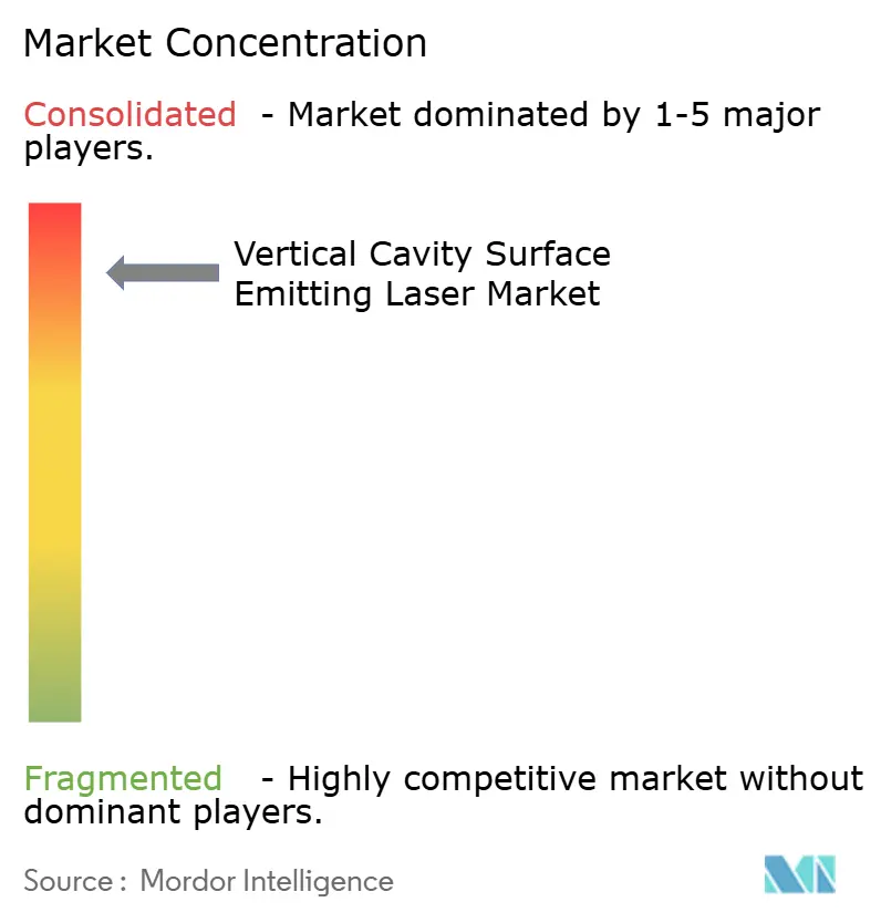
Global epitaxial capacity is moderately concentrated, with the top five companies accounting for approximately 68%. However, downstream packaging remains fragmented, featuring more than 30 integrators. Incumbents extend their advantage through vertically integrated wafer-to-module lines, which shave 14%-18% off the cost compared to fabless peers. Coherent added 14 patents on array thermal management in 2025, bringing its portfolio to 420 families and reinforcing automotive LiDAR moats.
Entrants face a cap on gross margins at 32% due to licensing fees of USD 0.18-0.24 per die for distributed Bragg reflector and oxide-aperture know-how, especially in the absence of cross-licenses. These licensing fees significantly impact the profitability of new players in the market, creating a challenging environment for those without established partnerships or proprietary technologies. Meanwhile, gallium nitride on silicon competitors are luring augmented-reality and medical buyers by slashing visible-light emitter prices by as much as 28%. This aggressive pricing strategy is encouraging buyers to diversify their supplier base, potentially reshaping the competitive landscape in these application areas.
Single-mode architectures for 2-kilometer datacom links remain a white space because silicon photonics dominates today, yet several VCSEL suppliers have joined co-packaged optics consortia to co-develop switch-ASIC-mounted arrays that eliminate front-panel modules. These alliances could shift market share in high-bandwidth AI clusters, adding fresh momentum to the vertical cavity surface-emitting laser market.
Vertical Cavity Surface Emitting Laser Industry Leaders
-
Coherent Corporation
-
Lumentum Operations LLC
-
Hamamatsu Photonics KK
-
TRUMPF Group
-
ams OSRAM AG
- *Disclaimer: Major Players sorted in no particular order
Vertical Cavity Surface Emitting Laser Market Companies Covered in this Report
- Coherent Corporation
- Lumentum Operations LLC
- ams OSRAM AG
- TRUMPF Group
- Broadcom Inc.
- Hamamatsu Photonics KK
- HLJ Technology Co. Ltd
- Teledyne FLIR Systems Inc.
- Vertilite Inc.
- Leonardo Electronics US
- Santec Corporation
- IQE plc
- WIN Semiconductors Corp.
- Bandwidth10 Inc.
- VERTILAS GmbH
- Ushio America Inc.
- Inneos LLC
- Frankfurt Laser Company
- Alight Technologies ApS
Market Opportunities and Future Outlook
A key whitespace is the migration from front-panel optics to near-package and co-packaged optical architectures inside AI-focused data centers, where VCSEL-based short-reach links compete on energy per bit and integration density for sub-300 meter fabrics. Recent actions by named suppliers reinforce this direction. In March 2026, Lumentum announced a new US manufacturing initiative anchored by acquiring a 240,000-square-foot facility in Greensboro, North Carolina from Qorvo to produce indium phosphide optical devices and ultra-high-power lasers for AI data centers. NVIDIA also announced strategic partnerships with both Lumentum and Coherent to expand capacity and R&D for next-generation optics technology.
Another opportunity is scaling automotive-grade multi-junction arrays and eye-safer wavelength choices for in-cabin and ADAS LiDAR. IEC 60825-1 constraints push OEMs and tier suppliers toward architectures that deliver range while maintaining Class 1 compliance. On the manufacturing side, cost and throughput improvement programs, including moves toward 6-inch wafer platforms and new patterning approaches highlighted by tool shipments into Asian VCSEL foundries, create room for differentiation through yield learning, packaging automation, and qualification depth across consumer, datacom, and automotive programs.
Recent Industry Developments in Vertical Cavity Surface Emitting Laser Market
- June 2026: NVIDIA announced a strategic partnership with Coherent to develop optics technology for next-generation data center architectures, including support for US-based manufacturing and capacity expansion. The initiative strengthens supply assurance for high-speed optical networking components used in AI clusters and increases competitive pressure on alternative short-reach interconnect approaches.
- March 2026: NVIDIA announced a strategic partnership with Lumentum focused on advancing optics technology and expanding capacity, supported by a USD 2 billion investment. This partnership reinforces domestic production priorities for critical laser components and aligns Lumentum product roadmaps with hyperscale AI interconnect requirements.
- June 2024: TRUMPF Photonic Components highlighted VCSEL-based laser heating approaches for battery electrode manufacturing, citing reductions in operational expenditure and CO2 footprint. The industrial processing use case broadens demand beyond consumer sensing and datacom by linking VCSEL deployments to manufacturing efficiency programs.
Vertical Cavity Surface Emitting Laser Market Report Scope and Research Methodology
Market Definition and Coverage
This market covers revenues generated from vertical-cavity surface-emitting laser (VCSEL) devices sold into commercial and government use cases, where demand is created by sensing, short-reach datacom, and other optical functions that need compact laser sources.
Scope exclusions: It excludes downstream module assembly and system integration value (for example, full camera modules or LiDAR systems) when those revenues are not attributable to the VCSEL device itself.
Segments Covered in This Report
- By Wavelength
- Red (650–750 nm)
- Near-Infrared (750–1400 nm)
- Shortwave-Infrared (1400–3000 nm)
- By Die Size
- 0.02 – 0.06 mm²
- 0.06 – 0.4 mm²
- 0.4 – 1.3 mm²
- 1.0 – 7.5 mm²
- By End-User Industry
- Telecom
- Mobile and Consumer
- Automotive
- Medical
- Industrial
- Aerospace and Defense
- By Application
- Datacom
- Facial Recognition and Depth Camera
- Gesture Recognition
- Proximity Sensing
- Laser Autofocus
- Iris Scan
- Medical Diagnostics
- ADAS LiDAR
- Industrial Processing
- Optical Mouse
- Other Application
- By Geography
- North America
- United States
- Canada
- Mexico
- Europe
- Germany
- United Kingdom
- France
- Russia
- Rest of Europe
- Asia-Pacific
- China
- Japan
- India
- South Korea
- Australia
- Rest of Asia-Pacific
- Middle East and Africa
- Middle East
- Saudi Arabia
- United Arab Emirates
- Rest of Middle East
- Africa
- South Africa
- Egypt
- Rest of Africa
- Middle East
- South America
- Brazil
- Argentina
- Rest of South America
- North America
Data Sources, Market Sizing, and Validation
Desk Research
For desk research, we start by building a clean fact base on the optoelectronics supply chain and on where VCSELs are actually deployed. Public sources such as the US International Trade Commission trade statistics, UN Comtrade, the US Patent and Trademark Office, IEEE and other peer-reviewed journals, and standards bodies and industry groups in optics and telecom are used to set context on technology direction and adoption.
We then connect those signals with company disclosures such as annual reports, earnings commentary, and investor presentations, plus reputable press coverage on data center buildouts, smartphone sensing changes, and automotive ADAS roadmaps. A limited set of paid database subscriptions is also used for company financials and intelligence, patent lookups, and import and export shipment-level checks where available, which helps cross-check volumes and pricing logic. These sources are illustrative only, and many other public references were also used for data collection, validation, and clarification during the work.
Primary Interviews and Surveys
Primary work focuses on interviews and structured questionnaires with VCSEL ecosystem participants, including component suppliers, wafer and epitaxy related experts, module makers, and buyers across consumer electronics, datacom, automotive, and industrial uses. We cover APAC, EMEA, and the Americas so that regional demand shifts, qualification cycles, and pricing movements are not overgeneralized from one geography. Inputs from these discussions are used to confirm adoption timing, realistic ASP ranges, and how mix changes between sensing and datacom affect revenue.
Distribution of primary research fieldwork respondents
| Company type | Respondent position | Region |
|---|---|---|
| Top tier: 38% | CXOs: 12% | APAC: 49% |
| Mid tier: 48% | Functional/Unit leaders: 32% | EMEA: 33% |
| Smaller Players: 14% | Managers: 56% | Americas: 18% |
Market-Sizing & Forecasting
Sizing starts with a top-down build where end-use demand pools are reconstructed by linking VCSEL-relevant application volumes to penetration assumptions and price curves. In practice, this means we map adoption in areas like 3D sensing and proximity functions in consumer devices, short-reach optical interconnect needs in data centers, and emerging VCSEL use in ADAS and LiDAR, and then translate those into device value using realistic ASP bands.
To keep the totals grounded, the results are corroborated with selective bottom-up approximations, such as sampled supplier revenue splits, channel checks on typical module content, and sanity checks on unit volumes implied by application ramps. Key model inputs include VCSEL wavelength mix (red, near-infrared, and shortwave-infrared), die size mix, average selling price progression, regional shipment mix, and adoption timing by end-user industry, which are adjusted when primary feedback shows a different qualification or ramp pattern. Forecasting leans on scenario analysis supported by a small set of macro and industry drivers, and then the scenarios are filtered through expert consensus on timing for device refresh cycles and data center optics upgrades. Where bottom-up signals are incomplete, gaps are handled using conservative interpolation based on adjacent application behavior and confirmed pricing ranges.
Data Validation & Update Cycle
Validation is done through a set of cross-checks that compare the modeled totals against independent signals, including regional demand direction, observed price movement patterns, and the implied mix between sensing and datacom. When outliers show up, assumptions are revisited, and selective experts are re-contacted to confirm whether the variance is caused by timing, scope, or a real market shift.
Before sign-off, the work goes through multi-step analyst reviews that look for arithmetic errors, inconsistent unit conversions, and unrealistic adoption curves by region. Reports are refreshed annually, and interim updates are performed when material events occur, such as major capacity changes or step shifts in a large end-market. Right before delivery, a final review pass is completed so clients receive the latest updated view.
Mordor Intelligence's Vertical Cavity Surface Emitting Laser Market Size Compared Against Other Published Estimates
Published VCSEL market numbers often look inconsistent because different studies count different parts of the value chain and then apply different assumptions for adoption timing and pricing. Variation also comes from how each publisher treats newer use cases like datacom interconnects and automotive sensing, which can ramp unevenly by region.
The main gap comes from whether revenues are counted at the VCSEL device level or whether packaged modules and adjacent optical components are blended into the total, and in this study Mordor Intelligence keeps the value strictly tied to the VCSEL device with ASPs and mix shifts cross-checked by wavelength, die size, and end-use adoption signals.
Benchmark comparison
| Source | Market Size | Gaps in Research Methodology |
|---|---|---|
| Mordor Intelligence | USD 2.94 B (2026) | |
| Regional Consultancy A | USD 1.30 B (2024) | Uses a narrower demand view that is heavily weighted to sensing, and it typically assumes slower ASP expansion and fewer datacom and automotive ramps in the base case. |
| Trade Journal B | USD 2.82 B (2024) | Often mixes shipment-based reporting with revenue sizing, and the conversion to value can depend on broad average prices that do not fully reflect die size and wavelength mix changes. |
Taken together, the spread is largely explained by scope and by how pricing and mix are treated over time. Our approach stays traceable because each major end-use ramp is linked to a clear adoption driver, and the revenue build is repeatedly checked against practical volume and ASP ranges before finalizing the totals.
Key Questions Answered in the Report
What is the current value of the vertical cavity surface emitting laser market?
The market reached USD 2.94 billion in 2026 and is projected to hit USD 6.91 billion by 2031.
Which application is growing fastest for VCSELs?
ADAS LiDAR leads with a 20.56% CAGR through 2031 as automakers adopt solid-state depth sensing to meet safety mandates.
Why are shortwave-infrared VCSELs gaining traction?
IEC 60825 Class 1 limits allow higher optical output at 1,550 nanometers, providing longer range and safer operation for automotive cabin monitoring.
How are hyperscale data centers using VCSEL technology?
Operators deploy 200 gigabit-per-lane multimode links and co-packaged optics to support bandwidth-intensive AI training clusters with lower power budgets.
Which region is expected to record the highest growth rate?
The Middle East projects a 19.73% CAGR due to sovereign investments in localized AI infrastructure.
What manufacturing hurdle limits long-wavelength VCSEL supply?
Indium phosphide epitaxial yields remain below 78%, raising die costs and constraining 1.3 µm and 1.55 µm device availability.