| Study Period | 2019 - 2030 |
| Market Size (2025) | USD 0.77 Billion |
| Market Size (2030) | USD 1.05 Billion |
| CAGR (2025 - 2030) | 6.35 % |
| Fastest Growing Market | Asia Pacific |
| Largest Market | Asia Pacific |
| Market Concentration | Medium |
Major Players
*Disclaimer: Major Players sorted in no particular order |

Thin Wafer Processing And Dicing Equipment Market Analysis
The Thin Wafer Processing And Dicing Equipment Market size is estimated at USD 0.77 billion in 2025, and is expected to reach USD 1.05 billion by 2030, at a CAGR of 6.35% during the forecast period (2025-2030).
The semiconductor industry is experiencing significant transformation driven by massive investments in manufacturing infrastructure and technological advancement. Global semiconductor market revenues are projected to reach USD 676 billion in 2022, reflecting the industry's robust growth trajectory and increasing demand across various applications. Major industry players are making substantial investments to expand their manufacturing capabilities, exemplified by Intel's announcement in 2023 to invest up to EUR 80 billion in the European Union's semiconductor value chain over the next decade, focusing on research and development, production, and packaging technologies.
The thin wafer processing landscape is witnessing a notable shift towards more specialized applications and advanced manufacturing processes. Manufacturers are increasingly focusing on developing ultra-thin wafers for three-dimensional integrated circuits, which are becoming essential in space-constrained applications such as portable consumer electronics, sensors, and industrial products. The industry is seeing particular advancement in wafer thinning technologies, with some manufacturers achieving thickness reductions to 10-50 micrometers, enabling improved thermal management and enhanced performance in various electronic devices.
The manufacturing infrastructure is undergoing substantial expansion, particularly in 200mm and 300mm fab capabilities. According to SEMI, 200mm fab equipment spending reached USD 5.3 billion in 2021, with manufacturers worldwide aiming to boost 200mm fab capacity by 21% to reach 6.9 million wafers per month by the end of 2024. The industry is also witnessing significant development in 300mm wafer fabrication facilities, with the number of operational 300mm wafer fabs expected to exceed 130 globally by 2024, indicating substantial investment in advanced manufacturing capabilities.
The industry is experiencing a notable trend towards silicon-carbide (SiC) wafer production and processing, driven by increasing demands from electric vehicle manufacturers and renewable energy applications. Manufacturers are investing in new semiconductor wafer processing equipment and technologies to handle these specialized materials, with several companies transitioning from 6-inch to 8-inch SiC wafer production to improve efficiency and reduce costs. This transition is accompanied by developments in plasma dicing and stealth dicing technologies, which are becoming increasingly important for processing these advanced materials while maintaining high quality and yield rates.
Thin Wafer Processing And Dicing Equipment Market Trends
Increasing Demand for Smart Cards, RFID Technology, and Automotive Power ICs
The increasing adoption of smart cards and RFID technology across various industries is driving significant demand for wafer handling equipment and wafer grinding equipment. In the retail sector, RFID technology has become crucial for improving inventory accuracy and supporting processes like store fulfillment and buy-online-pick-up-in-store (BOPIS) operations. The healthcare industry has also witnessed increased RFID adoption, particularly in tracking and ensuring the safety of vaccines and pharmaceutical products. The World Health Organization's estimation that one in every ten medical products across low- and middle-income countries are counterfeit has led to widespread implementation of RFID tracking systems, with major pharmaceutical companies like Pfizer and GlaxoSmithKline (GSK) incorporating RFID inlays in their product packaging to combat counterfeiting.
The automotive sector's transformation towards electric and autonomous vehicles has created substantial demand for power semiconductor components with sophisticated conversion schemes that decrease power consumption and heat. The advancement in automotive power ICs has been further accelerated by breakthrough innovations in semiconductor technology, such as IBM's 2nm chip technology that delivers 45% better performance and 75% lower energy consumption compared to 7nm node chips. This technological progression is particularly significant for electric vehicle applications, where power management and efficiency are crucial. The integration of multiple features on single chips and the trend toward 3D circuit architecture built onto ultra-thin silicon wafers has become essential for meeting the demanding requirements of modern automotive electronics, particularly in hybrid and electric cars where consumer demand for constant connectivity drives the need for more sophisticated semiconductor solutions. These advancements necessitate the use of specialized wafer dicing saw and IC packaging equipment to ensure precision and efficiency in production.
Understand The Key Trends Shaping This Market
Download PDF
Segment Analysis: By Equipment Type
Thinning Equipment Segment in Thin Wafer Processing and Dicing Equipment Market
The thinning equipment segment continues to dominate the thin wafer processing and dicing equipment market, holding approximately 65% market share in 2024. This significant market position is primarily driven by the increasing demand for memory, CMOS image sensors, power SiC components, and LED applications. The segment's growth is further bolstered by the rising need for miniaturization associated with enhanced performance in mobile devices and other consumer products. Advanced automation in wafer grinding equipment has enabled manufacturers to achieve the highest possible quality levels while reducing wafer thicknesses to less than 0.050 mm. The segment's dominance is also attributed to the widespread adoption of chemical-mechanical planarization (CMP) and other advanced technologies that effectively remove edge chipping and microcracking caused by standard grinding processes, particularly in memory and logic applications.
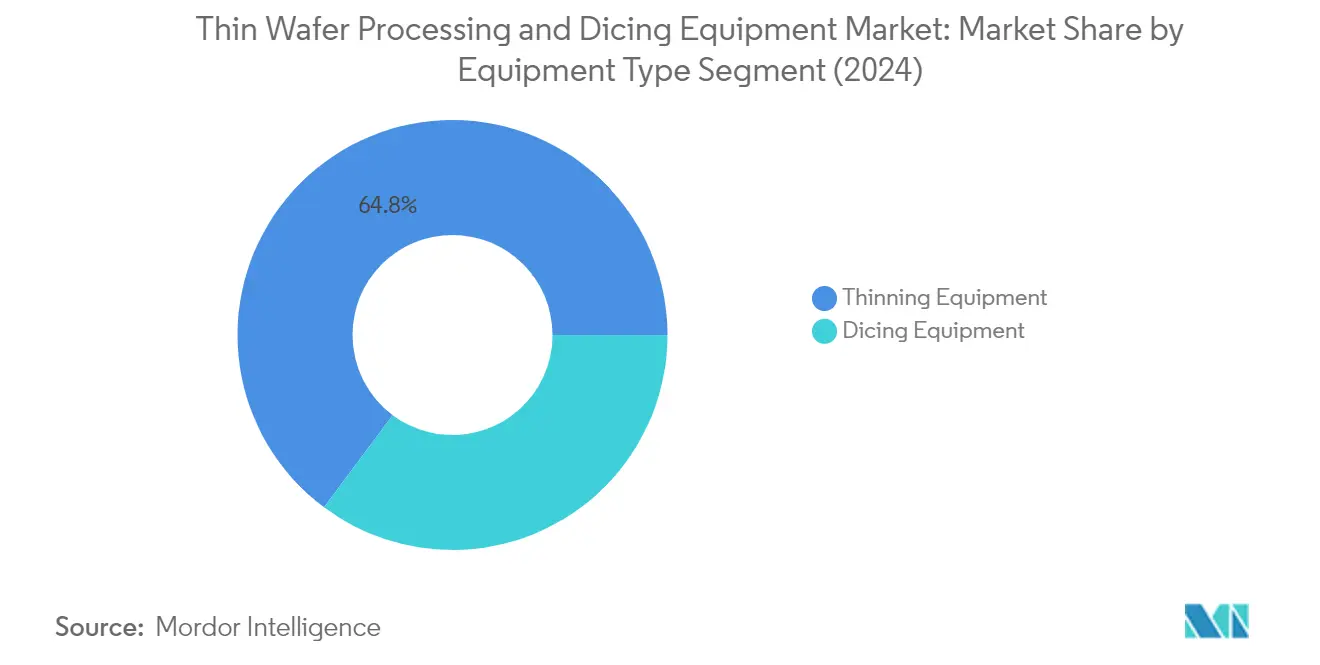
Dicing Equipment Segment in Thin Wafer Processing and Dicing Equipment Market
The dicing equipment segment is experiencing the fastest growth in the market, with an expected growth rate of approximately 7% from 2024 to 2029. This accelerated growth is driven by increasing demand for accurate dicing/cutting, grinding, and polishing among end-user sectors. The segment's expansion is supported by technological advancements enabling the dicing blade industry to venture into new application areas. The growth is particularly notable in plasma dicing applications, which are gaining prominence due to their ability to reduce the distance between chips on the scribe line and increase the number of chips per wafer. The segment is also benefiting from innovations in stealth dicing technology, which is becoming increasingly important for high-speed, high-quality dicing of ultra-thin semiconductor wafers, particularly in MEMS device production. The use of wafer dicing saw technology is pivotal in achieving precision and efficiency in these applications.
Segment Analysis: By Application
CMOS Image Sensors Segment in Thin Wafer Processing and Dicing Equipment Market
The CMOS image sensors segment dominates the thin wafer processing and dicing equipment market, holding approximately 59% market share in 2024. This significant market position is driven by the increasing integration of advanced imaging capabilities in smartphones, automotive applications like backup cameras and advanced driver assistance systems (ADAS), and emerging applications in security and medical imaging. The demand is further bolstered by the trend toward backside-illuminated (BIS) image sensor technology, which requires sophisticated wafer thinning processes to achieve optimal performance. Major manufacturers are expanding their production capacities and investing in new facilities to meet the growing demand for CMOS image sensors in applications ranging from consumer electronics to industrial and automotive sectors.
MEMS Devices Segment in Thin Wafer Processing and Dicing Equipment Market
The MEMS devices segment is experiencing the fastest growth in the thin wafer processing and dicing equipment market, with an expected growth rate of approximately 7% between 2024 and 2029. This rapid growth is attributed to the expanding applications of MEMS in diverse fields including wearable devices, smartphones, automotive sensors, and IoT devices. The adoption of stealth dicing technology has become particularly significant in MEMS manufacturing, as it offers superior cutting quality without debris contamination, which is crucial for sensitive MEMS structures. The segment's growth is further supported by increasing investments in MEMS manufacturing capabilities and the development of new applications in areas such as autonomous vehicles, industrial automation, and healthcare monitoring devices.
Remaining Segments in Application Market Segmentation
The remaining segments, including Power Devices, Memory and Logic (TSV), and RFID, each play vital roles in shaping the thin wafer processing and dicing equipment market. The power devices segment is particularly significant in supporting the growing electric vehicle market and renewable energy sectors. The Memory and Logic segment is crucial for advanced packaging technologies and 3D integration, while the RFID segment serves essential applications in retail, logistics, and security systems. These segments are experiencing varying levels of growth driven by their respective end-use applications, with power devices showing strong momentum due to electrification trends, while RFID maintains steady growth through expanding applications in supply chain management and contactless technologies.
Segment Analysis: By Wafer Size
8 inch Segment in Thin Wafer Processing and Dicing Equipment Market
The 8-inch wafer segment dominates the thin wafer processing and dicing equipment market, commanding approximately 36% market share in 2024, while also exhibiting the strongest growth trajectory with a projected growth rate of around 7% from 2024-2029. This segment's leadership position is driven by its widespread application across almost all types of integrated circuit production, including CMOS ICs, RFIDs, memory and logic, power devices, MEMS devices, and sensors. The versatility and cost-effectiveness of 8-inch wafers make them particularly attractive for manufacturers, as many electronic devices are built on ICs fabricated on 200mm wafers due to favorable pricing factors. Major semiconductor companies are actively expanding their 8-inch fab capabilities to address the growing demand, with significant investments being made in new facilities and capacity expansions. The segment's growth is further supported by the increasing adoption of 8-inch wafers in emerging technologies such as 5G, IoT, and automotive electronics, while also maintaining strong demand in traditional applications. The role of wafer handling equipment in managing these wafers efficiently is crucial to sustaining this growth.
Remaining Segments in Wafer Size Market Segmentation
The market's other segments include less than 4 inch, 5 inch and 6 inch, and 12 inch wafers, each serving specific industry needs and applications. The 5-inch and 6-inch segment maintains significant market presence due to its widespread use in RF devices, power semiconductors, MEMS, and sensor applications, particularly in the automotive and consumer electronics sectors. The less than 4-inch segment continues to serve niche applications in research and development, as well as specific industrial applications requiring smaller wafer sizes. The 12-inch segment, while representing the most advanced technology, primarily caters to high-end applications in memory, logic, and advanced semiconductor devices, with major foundries and integrated device manufacturers driving its adoption. These segments collectively complement the market by addressing diverse industry requirements across different technology nodes and applications, from legacy systems to cutting-edge semiconductor devices. The integration of semiconductor wafer processing equipment is essential in ensuring the efficiency and precision of these processes.
Thin Wafer Processing and Dicing Equipment Market Geography Segment Analysis
Thin Wafer Processing and Dicing Equipment Market in North America
North America represents a significant market for thin wafer processing and dicing equipment, driven by the region's prominence in semiconductor manufacturing equipment, design, and research activities. The United States and Canada form the key markets in this region, with both countries showing a strong commitment to strengthening their semiconductor manufacturing equipment capabilities through various initiatives and investments. The region's market is particularly influenced by the growing demand for semiconductors in automotive electronics, consumer devices, and emerging technologies like artificial intelligence and machine learning applications.
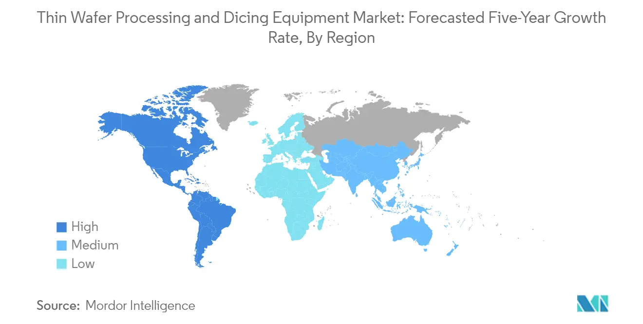
Thin Wafer Processing and Dicing Equipment Market in United States
The United States dominates the North American market as the largest country for thin wafer processing and dicing equipment. With approximately 89% market share in North America by 2024, the country maintains its leadership through significant investments in semiconductor manufacturing equipment and research activities. The US semiconductor industry maintains market leadership in activities that are most intensive in R&D, including chip design, EDA, and core IP, and manufacturing equipment. The government's recognition of the importance of bolstering America's semiconductor supply chains has led to various initiatives supporting domestic chip production and innovation, particularly focusing on enhancing the country's position in the global semiconductor ecosystem.
Thin Wafer Processing and Dicing Equipment Market in Canada
Canada emerges as the fastest-growing market in North America, with a projected growth rate of approximately 7% during 2024-2029. The country is strategically positioning itself in the semiconductor manufacturing equipment market through various initiatives, including the formation of the Semiconductor Council of Canada and the implementation of comprehensive roadmaps for semiconductor development. Canada's focus on developing and manufacturing chips for various applications, including automotive, healthcare, consumer electronics, and smart agriculture, demonstrates its commitment to becoming a significant player in the global semiconductor landscape. The country's emphasis on strengthening its semiconductor ecosystem through partnerships, research facilities, and government support programs is expected to drive sustained growth in the thin wafer processing and dicing equipment market.
Thin Wafer Processing and Dicing Equipment Market in Europe
The European market for thin wafer processing and dicing equipment is characterized by a strong focus on automotive applications, clean energy initiatives, and advanced manufacturing capabilities. The region encompasses key markets including the United Kingdom, Germany, France, Spain, and Italy, each contributing uniquely to the semiconductor ecosystem. European countries are actively investing in semiconductor research and development, with particular emphasis on power semiconductors and advanced packaging technologies. The region's strategic initiatives to reduce dependency on external semiconductor supplies and strengthen domestic manufacturing capabilities are shaping market dynamics.
Thin Wafer Processing and Dicing Equipment Market in United Kingdom
The United Kingdom stands as the largest market in Europe, commanding approximately 30% of the regional market share in 2024. The country's strength lies in its advanced semiconductor manufacturing capabilities and research initiatives, particularly in plasma dicing technologies and wafer processing solutions. The UK's focus on strengthening semiconductor supply chains through strategic partnerships and domestic manufacturing initiatives has positioned it as a key player in the European market. The country's semiconductor industry benefits from strong collaboration between academic institutions, research organizations, and manufacturing facilities.
Thin Wafer Processing and Dicing Equipment Market in Germany
Germany emerges as the fastest-growing market in Europe, with a projected growth rate of approximately 7% during 2024-2029. The country's market is primarily driven by its robust automotive industry and increasing adoption of electric vehicles, which require advanced semiconductor components. Germany's strategic focus on developing next-generation semiconductor technologies and its strong industrial base contribute to its rapid market growth. The country's emphasis on Industry 4.0 initiatives and automation technologies further supports the expansion of the thin wafer processing and dicing equipment market.
Thin Wafer Processing and Dicing Equipment Market in Asia Pacific
Asia Pacific represents the largest regional market for thin wafer processing and dicing equipment, with a diverse landscape encompassing major semiconductor manufacturing hubs. The region includes key markets such as China, Japan, Australia, and India, each contributing to the semiconductor ecosystem through various initiatives and investments. The market is characterized by significant investments in semiconductor manufacturing facilities, particularly in China and Japan, while emerging economies like India are developing their semiconductor capabilities through strategic initiatives and partnerships.
Thin Wafer Processing and Dicing Equipment Market in China
China dominates the Asia Pacific market as both the largest and fastest-growing country in the region. The country's semiconductor industry has experienced unprecedented growth in microsystems and semiconductor infrastructure over the past decade. China's focus on becoming self-sufficient in semiconductor manufacturing, coupled with significant investments in research and development, has positioned it as a key player in the global market. The country's strong manufacturing base and growing domestic demand for electronic devices continue to drive market expansion.
Thin Wafer Processing and Dicing Equipment Market in Latin America
The Latin American market for thin wafer processing and dicing equipment is characterized by growing adoption of semiconductor technologies across various industries, particularly in the automotive and consumer electronics sectors. Mexico and Brazil represent the key markets in this region, with Mexico emerging as both the largest and fastest-growing country. The region's market is driven by increasing investments in manufacturing facilities, particularly in Mexico's automotive sector, while Brazil shows promising growth potential through its focus on renewable energy applications and consumer electronics.
Thin Wafer Processing and Dicing Equipment Market in Middle East & Africa
The Middle East & Africa market for thin wafer processing and dicing equipment is experiencing steady growth, driven by increasing investments in semiconductor technologies and electronic manufacturing capabilities. Saudi Arabia and South Africa represent the key markets in this region, with Saudi Arabia emerging as both the largest and fastest-growing country. The region's market is characterized by growing investments in semiconductor manufacturing facilities and increasing adoption of advanced technologies across various industries, particularly in Saudi Arabia's Vision 2030 initiatives and South Africa's focus on renewable energy applications.
Get Analysis on Important Geographic Markets
Download PDF
Thin Wafer Processing And Dicing Equipment Industry Overview
Top Companies in Thin Wafer Processing and Dicing Equipment Market
The thin wafer processing and dicing equipment market is characterized by continuous product innovation from leading players like DISCO Corporation, SPTS Technologies, Plasma-Therm LLC, and Han's Laser Technology. Companies are focusing on developing advanced plasma dicing solutions, laser-induced systems, and automated processing equipment to meet the growing demand for thinner wafers. Strategic investments in R&D centers and manufacturing facilities, particularly in Asia-Pacific, demonstrate the industry's commitment to technological advancement. Market leaders are expanding their geographical presence through new office establishments and strategic partnerships, while simultaneously enhancing their service capabilities. The emphasis on developing comprehensive process solutions, including wafer breaking, expansion equipment, and integrated systems, showcases the industry's drive toward offering end-to-end solutions for semiconductor manufacturers.
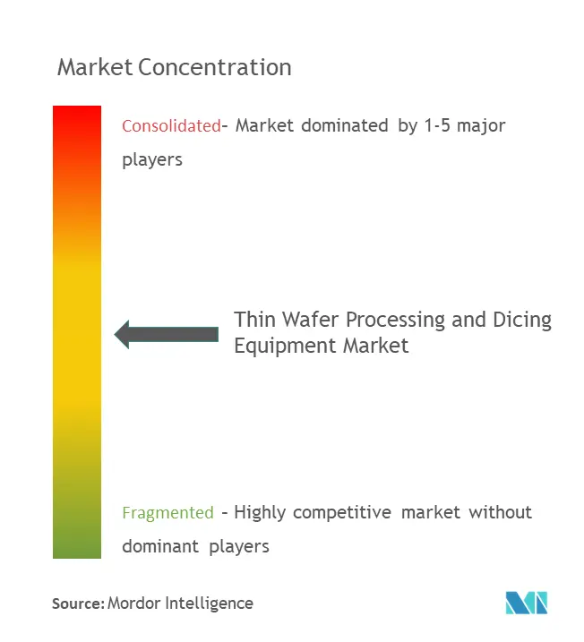
Market Dominated by Specialized Technology Leaders
The thin wafer processing and dicing equipment market exhibits a moderate level of consolidation, with a mix of global technology conglomerates and specialized equipment manufacturers. Japanese and European companies maintain significant market presence through their established technological expertise and long-standing relationships with semiconductor manufacturers. The industry has witnessed strategic acquisitions aimed at expanding technological capabilities, with companies like Plasma-Therm acquiring complementary businesses to enhance their product portfolios in areas such as PVD and RTP technologies.
The competitive landscape is shaped by companies' ability to provide customized solutions and maintain strong after-sales support networks. Market players are increasingly focusing on establishing regional manufacturing and R&D facilities to better serve local markets and reduce delivery times. The industry sees ongoing collaboration between equipment manufacturers and research institutions to develop next-generation processing technologies, particularly in emerging areas like stealth dicing and plasma-assisted processes.
Innovation and Service Excellence Drive Growth
Success in the thin wafer processing and dicing equipment industry increasingly depends on companies' ability to develop solutions that address the growing demand for thinner wafers while maintaining processing quality and yield rates. Incumbents are strengthening their market position by investing in advanced manufacturing capabilities, expanding their service networks, and developing specialized solutions for emerging applications like MEMS devices and power semiconductors. Companies are also focusing on building comprehensive quality management systems and obtaining relevant certifications to meet the stringent requirements of automotive and other high-reliability applications.
For new entrants and growing players, success lies in identifying and serving niche market segments while building strong technological capabilities. The industry's future will be shaped by companies' ability to address challenges in ultra-thin wafer handling, reduce processing costs, and develop solutions for next-generation semiconductor devices. Regulatory requirements related to environmental protection and hazardous materials are becoming increasingly important, requiring companies to invest in compliant technologies and processes. The concentration of end-users in the semiconductor industry necessitates strong relationship building and continuous innovation in processing solutions, including semiconductor manufacturing equipment and wafer bonding equipment.
Thin Wafer Processing And Dicing Equipment Market Leaders
-
Suzhou Delphi Laser Co. Ltd
-
SPTS Technologies Limited
-
Han's Laser Technology Industry Group
-
ASM Laser Separation International (ALSI) BV
-
Plasma-Therm LLC
- *Disclaimer: Major Players sorted in no particular order
Need More Details on Market Players and Competiters?
Download PDF
Thin Wafer Processing And Dicing Equipment Market News
- May 2024: ERS Electronic, the leader in thermal management solutions for semiconductor manufacturing, announced two new fully automatic machines from its Luminex product line. The machines, LUM300A1 and LUM300A2, are designed to handle 300 µm substrates. Both feature ERS’s state-of-the-art PhotoThermal debonding technology, which offers unparalleled flexibility, cost-effectiveness, and throughput for temporary bonding and debonding processes.
- December 2023: New York collaborated with tech giants IBM and Micron to invest USD 10 billion in an advanced chip research complex. This partnership aimed to establish a cutting-edge semiconductor research and development program, promising technological advancement and fostering growth in the semiconductor industry. Such progress will likely increase the demand for thin wafer processing and dicing equipment.
Thin Wafer Processing & Dicing Equipment Market Report - Table of Contents
1. INTRODUCTION
- 1.1 Study Assumptions and Market Definition
- 1.2 Scope of the Study
2. RESEARCH METHODOLOGY
3. EXECUTIVE SUMMARY
4. MARKET INSIGHTS
- 4.1 Market Overview
-
4.2 Industry Attractiveness Porter's Five Forces Analysis
- 4.2.1 Threat of New Entrants
- 4.2.2 Bargaining Power of Buyers
- 4.2.3 Bargaining Power of Suppliers
- 4.2.4 Threat of Substitute Products
- 4.2.5 Intensity of Competitive Rivalry
- 4.3 Industry Value Chain Analysis
- 4.4 Impact of COVID-19 Aftereffects and Other Macroeconomic Factors on the Market
5. MARKET DYNAMICS
-
5.1 Market Drivers
- 5.1.1 Increasing Demand for Smart Cards, RFID Technology, and Automotive Power ICs
- 5.1.2 Increasing Need for Miniaturization of Semiconductors
-
5.2 Market Restraint
- 5.2.1 Manufacturing Challenges
6. MARKET SEGMENTATION
-
6.1 By Equipment Type
- 6.1.1 Thinning Equipment
- 6.1.2 Dicing Equipment
- 6.1.2.1 Blade Dicing
- 6.1.2.2 Laser Ablation
- 6.1.2.3 Stealth Dicing
- 6.1.2.4 Plasma Dicing
-
6.2 By Application
- 6.2.1 Memory and Logic (TSV)
- 6.2.2 MEMS Devices
- 6.2.3 Power Devices
- 6.2.4 CMOS Image Sensors
- 6.2.5 RFID
- 6.2.6 Others
-
6.3 By Wafer Thickness
- 6.3.1 750 micrometers
- 6.3.2 120 micrometers
- 6.3.3 50 micrometers
-
6.4 By Wafer Size
- 6.4.1 Less than 4 inches
- 6.4.2 5 inches and 6 inches
- 6.4.3 8 inches
- 6.4.4 12 inches
-
6.5 By Geography***
- 6.5.1 North America
- 6.5.2 Europe
- 6.5.3 Asia
- 6.5.4 Australia and New Zealand
- 6.5.5 Latin America
- 6.5.6 Middle East and Africa
7. COMPETITIVE LANDSCAPE
-
7.1 Company Profiles
- 7.1.1 Suzhou Delphi Laser Co. Ltd
- 7.1.2 SPTS Technologies Limited
- 7.1.3 Plasma-Therm LLC
- 7.1.4 Han's Laser Technology Industry Group Co. Ltd
- 7.1.5 ASM Laser Separation International (ALSI) BV
- 7.1.6 Disco Corporation
- 7.1.7 Tokyo Seimitsu Co, Ltd (Accretech)
- 7.1.8 Neon Tech Co. Ltd
- 7.1.9 Advanced Dicing Technologies Ltd
- 7.1.10 Panasonic Corporation
- 7.1.11 Hitachi High-Tech Corporation
- *List Not Exhaustive
8. INVESTMENT ANALYSIS
9. MARKET OPPORTUNITIES AND FUTURE TRENDS
**Subject to Availability
***In the final report, Asia, Australia, and New Zealand will be studied together as 'Asia Pacific'
You Can Purchase Parts Of This Report. Check Out Prices For Specific Sections
Get Price Break-up Now
Thin Wafer Processing And Dicing Equipment Industry Segmentation
The need for miniaturization toward small-sized, high-performing, and low-cost device configurations has created the need for thin wafers. Most of these reach below 100 µm or even 50 µm for applications such as memory and power devices. Moreover, wafer dicing is the process of separating the die from a semiconductor wafer after the wafer has been processed.
The thin wafer processing & dicing equipment market is segmented by equipment type (thinning equipment and dicing equipment [blade dicing, laser ablation, stealth dicing, and plasma dicing]), application (memory and logic, MEMS devices, power devices, CMOS image sensors, RFID, and others), wafer thickness (750 µm, 120 µm, and 50 µm), wafer size (less than 4 inches, 5 inches and 6 inches, 8 inches, and 12 inches), and geography (North America, Europe, Asia-Pacific, Latin America, and the Middle East and Africa). The report offers the market sizes and forecasts for all the above segments in value terms (USD).
| By Equipment Type | Thinning Equipment | ||
| Dicing Equipment | Blade Dicing | ||
| Laser Ablation | |||
| Stealth Dicing | |||
| Plasma Dicing | |||
| By Application | Memory and Logic (TSV) | ||
| MEMS Devices | |||
| Power Devices | |||
| CMOS Image Sensors | |||
| RFID | |||
| Others | |||
| By Wafer Thickness | 750 micrometers | ||
| 120 micrometers | |||
| 50 micrometers | |||
| By Wafer Size | Less than 4 inches | ||
| 5 inches and 6 inches | |||
| 8 inches | |||
| 12 inches | |||
| By Geography*** | North America | ||
| Europe | |||
| Asia | |||
| Australia and New Zealand | |||
| Latin America | |||
| Middle East and Africa | |||
Need A Different Region or Segment?
Customize Now
Thin Wafer Processing & Dicing Equipment Market Research FAQs
How big is the Thin Wafer Processing And Dicing Equipment Market?
The Thin Wafer Processing And Dicing Equipment Market size is expected to reach USD 0.77 billion in 2025 and grow at a CAGR of 6.35% to reach USD 1.05 billion by 2030.
What is the current Thin Wafer Processing And Dicing Equipment Market size?
In 2025, the Thin Wafer Processing And Dicing Equipment Market size is expected to reach USD 0.77 billion.
Who are the key players in Thin Wafer Processing And Dicing Equipment Market?
Suzhou Delphi Laser Co. Ltd, SPTS Technologies Limited, Han's Laser Technology Industry Group, ASM Laser Separation International (ALSI) BV and Plasma-Therm LLC are the major companies operating in the Thin Wafer Processing And Dicing Equipment Market.
Which is the fastest growing region in Thin Wafer Processing And Dicing Equipment Market?
Asia Pacific is estimated to grow at the highest CAGR over the forecast period (2025-2030).
Which region has the biggest share in Thin Wafer Processing And Dicing Equipment Market?
In 2025, the Asia Pacific accounts for the largest market share in Thin Wafer Processing And Dicing Equipment Market.
What years does this Thin Wafer Processing And Dicing Equipment Market cover, and what was the market size in 2024?
In 2024, the Thin Wafer Processing And Dicing Equipment Market size was estimated at USD 0.72 billion. The report covers the Thin Wafer Processing And Dicing Equipment Market historical market size for years: 2019, 2020, 2021, 2022, 2023 and 2024. The report also forecasts the Thin Wafer Processing And Dicing Equipment Market size for years: 2025, 2026, 2027, 2028, 2029 and 2030.
Our Best Selling Reports
Thin Wafer Processing And Dicing Equipment Market Research
Mordor Intelligence offers a comprehensive analysis of the thin wafer processing and dicing equipment market. We leverage our extensive experience in semiconductor manufacturing equipment research to provide valuable insights. Our detailed report, available as an easy-to-download PDF, covers semiconductor wafer processing equipment trends and technological advancements. It encompasses the full range of equipment, from wafer handling equipment to wafer grinding equipment, offering stakeholders crucial insights into industry dynamics.
The report extensively examines wafer dicing saw technologies, wafer bonding equipment innovations, and advanced packaging equipment developments. This provides valuable intelligence for industry participants. Our analysis focuses particularly on IC packaging equipment technologies and their evolving applications in the semiconductor manufacturing equipment market. Stakeholders gain access to detailed technical specifications, emerging technology assessments, and comprehensive industry forecasts. This enables informed decision-making and strategic planning in this rapidly evolving sector.