Market Trends of Thin Layer Deposition Industry
Increase in Demand for Microelectronics and Consumer Electronics to Fuel the Demand
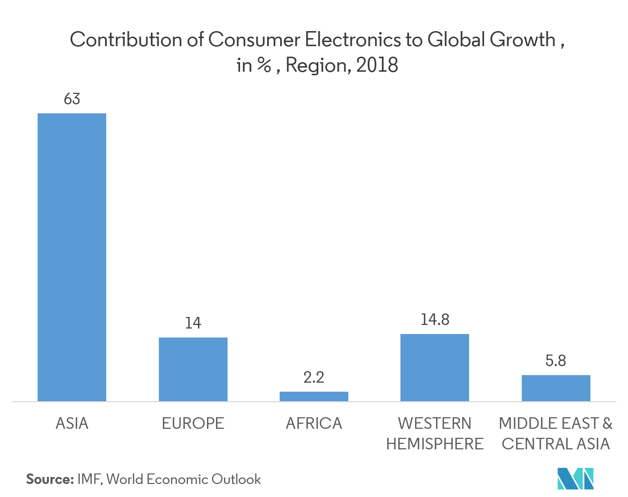
- The rise in the sale of microelectronics and consumer electronics is expected to fuel the demand for semiconductor ICs, during the forecast period. The increase in demand for semiconductor ICs is projected to improve the production capacity of semiconductor device manufacturers, which, in turn, may augment the demand for the atomic layer deposition market.
- Besides, governments and industry stakeholders are keenly following the advancements in the microelectronics industry, as these technologies might potentially disrupt and boost the Internet of Things. The industry has been investing in enhancing chip performance too. For e.g. in June 2018, Applied Materials Inc. announced a breakthrough in materials engineering, which accelerated chip performance in the AI and Big Data era. The company’s unique integrated materials solution combines dry clean, Atomic Layer Deposition (ALD), Physical Vapor Deposition (PVD), and Chemical Vapor Deposition (CVD) on the Endura platform, enabling the customers to quicken the adoption of cobalt.
- Many of the manufacturing companies prefer the atomic layer deposition technique to produce smaller components with comparatively low costs with the demand for miniaturization growing every day. As device requirements push toward smaller and more spatially demanding structures, ALD has demonstrated potential advantages over alternative deposition methods, such as chemical vapor deposition (CVD) and various physical vapor deposition (PVD) techniques, due to its conformality and control over materials thickness and composition. This broad adoption of ALD,CVD, PVD is expected to fuel the growth of the market studied.
Asia- Pacific Region to Dominate the Market
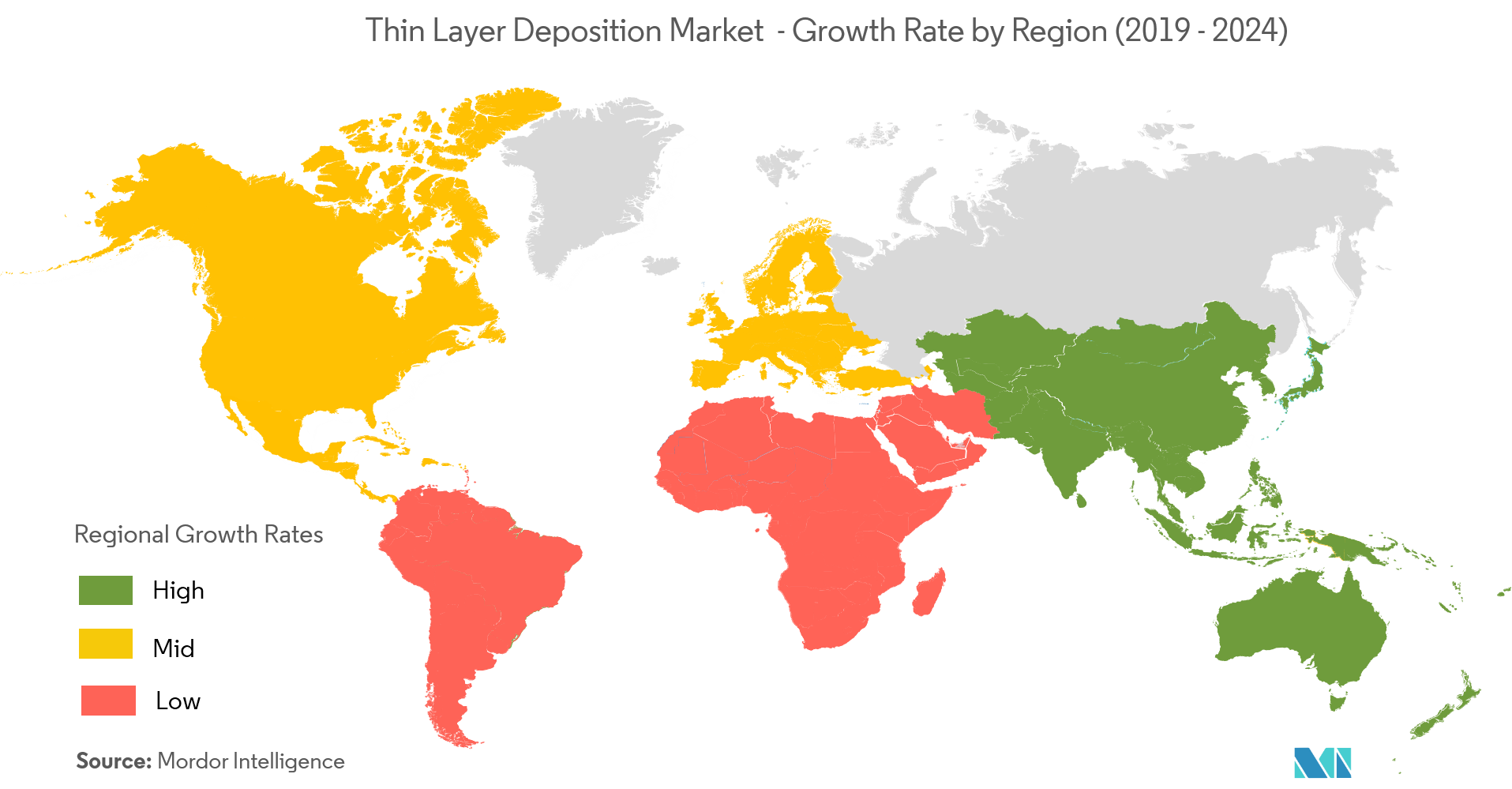
- Asia-Pacific accounted for the most significant market share in the thin layer deposition market. The growth of the regional market can be attributed to the progression of electronics and semiconductor industries, mainly in China. The deep-rooted electronics manufacturing bases in China, South Korea, and Taiwan led to an increased demand for deposition technologies.
- The rise in industrialization and increase in the number of end-user industries in developing economies, such as China and India, have offered numerous untapped opportunities. Moreover, China, Indonesia, Japan, South Korea, and Taiwan have led the thin layer deposition growth, due to increasing solar panel manufacturing and installations. For instance, on May 31, 2018, the Chinese government announced subsidy reductions for photovoltaic power generation, widely known as the 531 Policy.
- Moreover, the rising demand for electronic components in the automotive industry is anticipated to increase the demand for semiconductors, in the region. This, in turn, directly impacts the growth of the market studied, in a positive manner.


