
Semiconductor Wafer Polishing And Grinding Equipment Market Size and Share
Market Overview
| Study Period | 2020 - 2031 |
|---|---|
| Market Size (2026) | USD 1.67 Billion |
| Market Size (2031) | USD 2.22 Billion |
| Growth Rate (2026 - 2031) | 5.86 % |
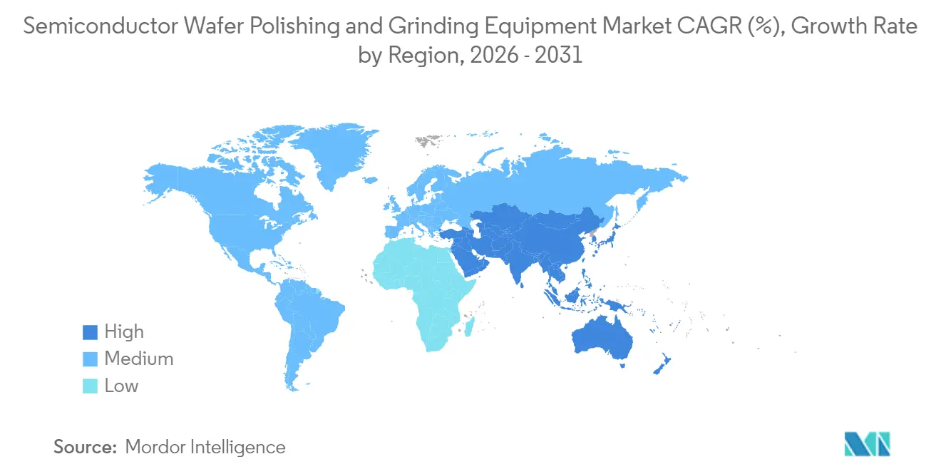
| Fastest Growing Market | Middle East and Africa |
| Largest Market | Asia Pacific |
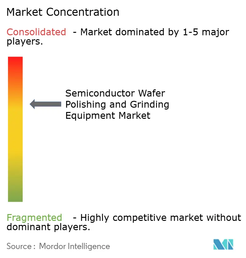
| Market Concentration | Medium |
Major Players *Disclaimer: Major Players sorted in no particular order Image © Mordor Intelligence. Reuse requires attribution under CC BY 4.0. | |
Semiconductor Wafer Polishing And Grinding Equipment Market Analysis by Mordor Intelligence
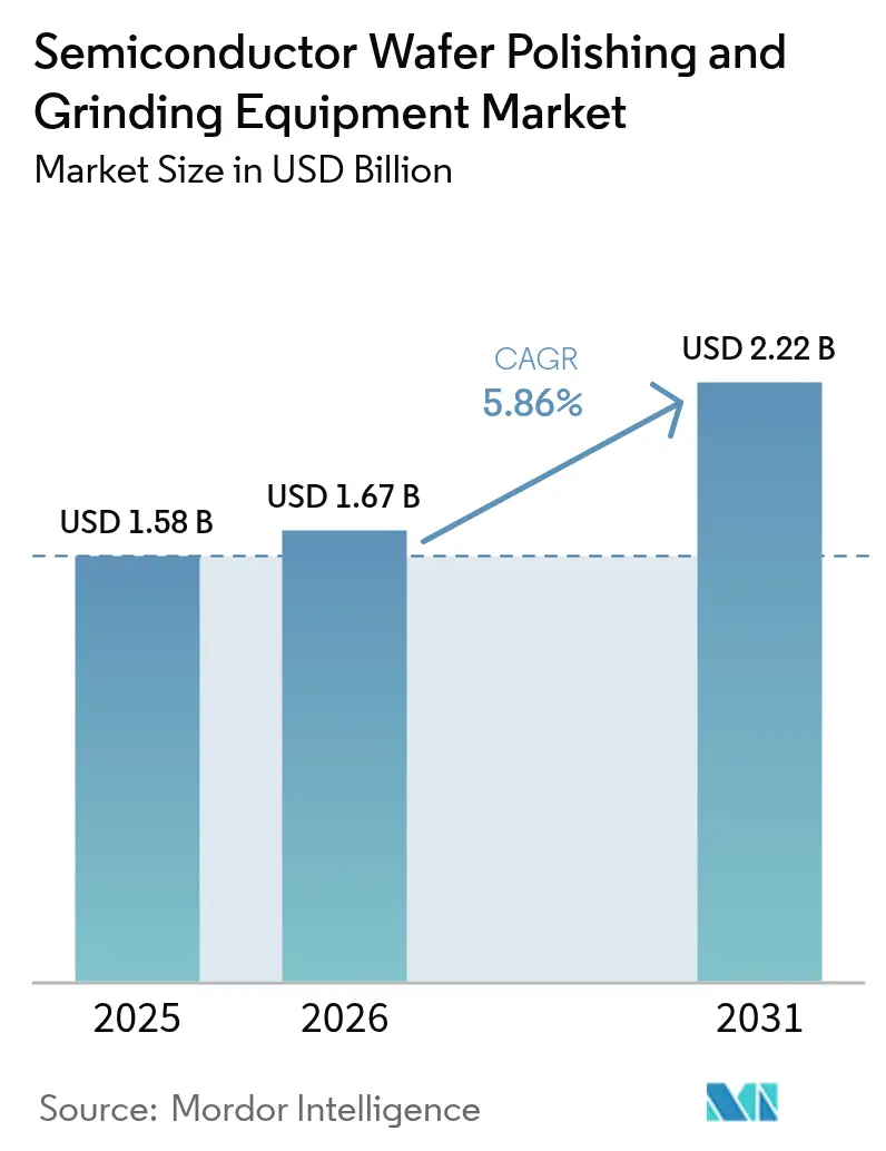
The semiconductor wafer polishing and grinding equipment market size is expected to grow from USD 1.58 billion in 2025 to USD 1.67 billion in 2026 and is forecast to reach USD 2.22 billion by 2031 at 5.86% CAGR over 2026-2031.Semiconductor Industry,” semiconductors.org">[1] During the period, capital spending on larger wafers, wide-bandgap materials, and automation tools has driven sustained order volumes for precision material-removal systems. Equipment suppliers scaled real-time process-control features to manage atomic-level tolerances, while AI-enabled diagnostics offset technician shortages and improved yield. Export-control rules reshaped sourcing strategies, prompting parallel investments in North America and Europe that reduced over-reliance on Asia and strengthened regional service footprints. Sustainability mandates also influenced tool selection, accelerating the shift toward slurry-free CMP pads and low-consumable grinding technologies.
Key Report Takeaways
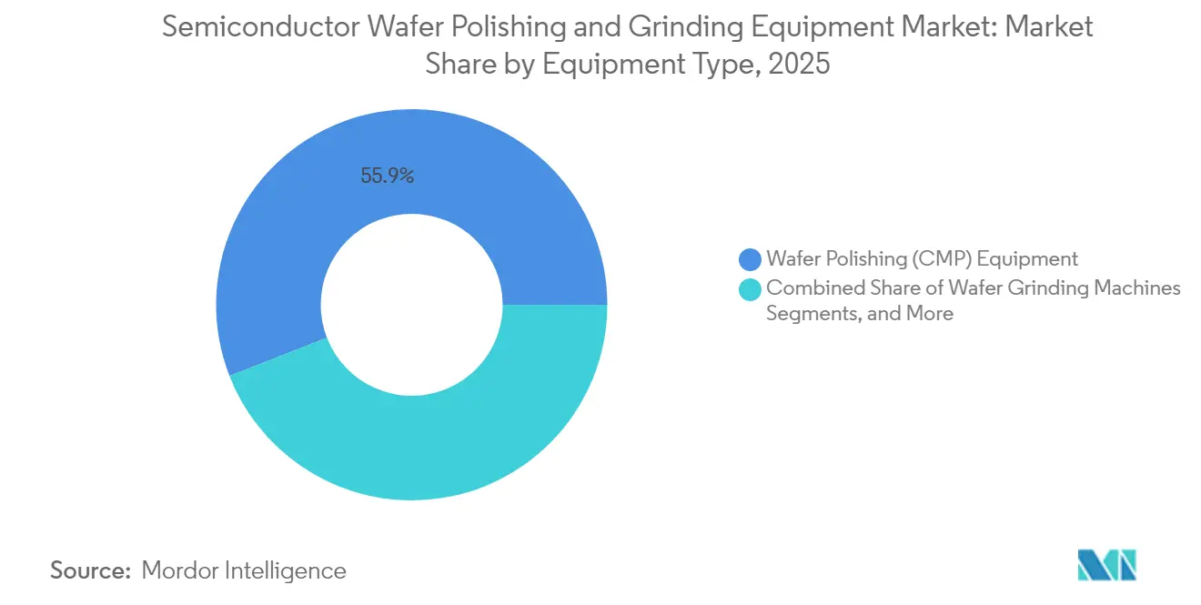
- By equipment type, Chemical Mechanical Polishing (CMP) led with 55.92% revenue share in 2025; integrated grinder-polisher tools are projected to expand at a 7.55% CAGR to 2031.
- By wafer size, 300 mm accounted for 61.88% of the semiconductor wafer polishing and grinding equipment market share in 2025, while the 450 mm and above segment is poised for an 10.84% CAGR through 2031.
- By technology, CMP tools commanded 55.92% revenue in 2025; edge-grinding and bevel-polishing solutions are advancing at an 8.56% CAGR over the forecast horizon.
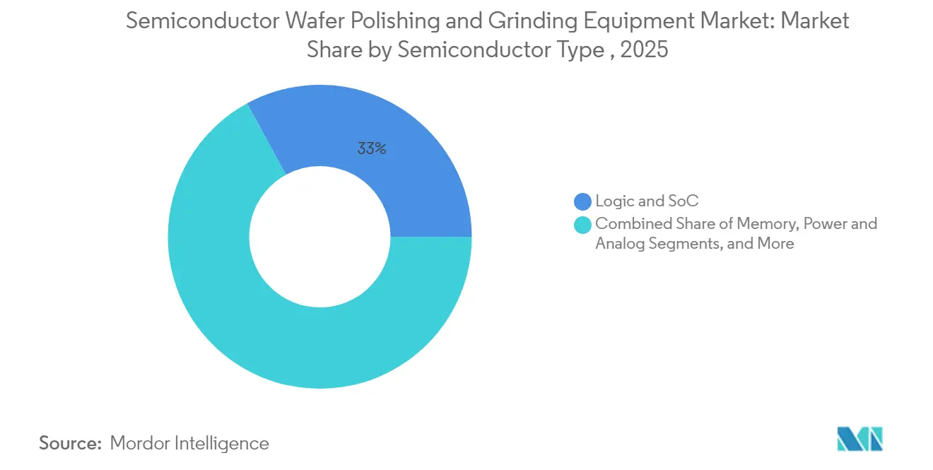
- By semiconductor type, logic and SoC devices held a 32.95% share in 2025, whereas SiC / GaN power devices are set for a 9.78% CAGR to 2031.
- By end-user, foundries represented 49.86% of demand in 2025, while OSAT and advanced-packaging facilities are growing at a 7.46% CAGR.
- By geography, Asia-Pacific dominated with 67.94% revenue in 2025; the Middle East and Africa region shows the fastest 8.84% CAGR from 2026-2031.
Note: Market size and forecast figures in this report are generated using Mordor Intelligence’s proprietary estimation framework, updated with the latest available data and insights as of 2026.
Market Trends and Insights
Drivers Impact Analysis of Semiconductor Wafer Polishing And Grinding Equipment Market*
| Driver | (~) % Impact on CAGR Forecast | Geographic Relevance | Impact Timeline |
|---|---|---|---|
| Growing consumption of consumer electronics with advanced-node chips | +1.2% | Asia-Pacific, spillover to North America and Europe | Medium term (2-4 years) |
| Miniaturization push driving demand for 300 mm and 450 mm CMP tools | +1.5% | Global concentration in Taiwan, South Korea, and Japan | Long term (≥ 4 years) |
| Foundry capacity investments in the U.S. and Europe under the CHIPS Act | +1.8% | North America, Europe | Medium term (2-4 years) |
| Transition to SiC/GaN power devices requires ultra-precision grinding | +1.3% | Global, early adoption in Japan, Germany, USA | Medium term (2-4 years) |
| Yield-enhancement needs for 3D-IC and heterogeneous integration | +0.9% | Global: Taiwan, South Korea, USA | Short term (≤ 2 years) |
| Sustainability mandates advancing slurry-free polishing technologies | +0.7% | Europe, North America, Japan | Long term (≥ 4 years) |
| Source: Mordor Intelligence | |||
Growing consumption of consumer electronics with advanced-node chips in Asia
Rapid uptake of flagship smartphones and AI-enabled wearables across China, India, and Southeast Asia accelerated demand for sub-3 nm devices that require atomically smooth wafer surfaces and defect densities measured in parts per billion. Local foundries expanded CMP and fine-grinding capacity despite export-license uncertainty, while tool makers introduced chlorine-free pads that met strict environmental codes without compromising planarity. As multi-core SoCs proliferated, process uniformity across diverse material stacks became critical, spurring investment in adaptive-control CMP systems tailored for heterogeneous layers.
Miniaturization push driving demand for 300 mm and 450 mm CMP tools
The search for cost-effective die density sustained 300 mm as the mainstream format, yet exploratory 450 mm development resurfaced because a larger blank yields 2.25 times more die area. Tool makers tackled the scale-up challenge by reinforcing platens, optimizing slurry distribution, and embedding in-situ metrology to maintain nanometer-level removal uniformity across wider surfaces. TSMC’s prototype 510 mm × 515 mm rectangular substrate hinted at an alternate path that could triple usable area without fully overhauling legacy tool architectures.
Foundry capacity investments in the U.S. and Europe under the CHIPS Act
Between 2024 and 2025, more than USD 450 billion of private projects were announced in the United States, while the European Chips Act mobilized EUR 43 billion to double the region’s output share by 2030. Both programs required localized CMP and grinding ecosystems that conform to tighter export-control rules and deliver rapid service response. Vendors responded by expanding U.S. refurbishment centers and EU demo labs, shortening lead times, and ensuring compliance with the Foreign Direct Product (FDP) regulations.
Transition to SiC/GaN power devices requires ultra-precision grinding
SiC and GaN wafers reached 16% penetration of power-device output in 2024 and are projected to exceed 32% by 2029, a shift that demanded harder wheels, ultrasonic assistance, and EDM-based non-contact methods to prevent subsurface damage. Material-removal rates lagged silicon by 30-50%, so tool builders prioritized process efficiency, integrating AI-driven spark-detection and coolant-flow analytics to safeguard wafer integrity and cut cycle time.
Restraints Impact Analysis of Semiconductor Wafer Polishing And Grinding Equipment Market*
| Restraint | (~) % Impact on CAGR Forecast | Geographic Relevance | Impact Timeline |
|---|---|---|---|
| High capital cost and long ROI cycle for 300 mm tools | -1.2% | Global, higher impact in emerging markets | Medium term (2-4 years) |
| Consumables cost inflation (pads, slurries, wheels) | -0.8% | Global | Short term (≤ 2 years) |
| Export controls and IP barriers limiting shipments to China | -1.4% | China with a global ripple | Medium term (2-4 years) |
| Skilled technician shortage for process setup and maintenance | -0.9% | Global, acute in North America and Europe | Long term (≥ 4 years) |
| Source: Mordor Intelligence | |||
High capital cost and long ROI cycle for 300 mm tools
A single 300 mm CMP platform carried a USD 3-5 million price tag in 2024, with facility upgrades adding USD 1-2 million, stretching payback beyond 4 years in lower-volume fabs. Smaller players delayed expansion and opted for refurbished or shared-capacity models, slowing overall tool uptake despite clear cost-per-die advantages at scale.
Export controls and IP barriers limiting shipments to China
The December 2024 U.S. interim rule expanded the FDP framework, cutting projected 2025 equipment shipments to China by up to 30% and forcing vendors to re-engineer modules that embed U.S. technology.[2] Chinese customers accelerated domestic tool programs, diversifying global demand but compressing margins for companies highly exposed to the market.
*Our forecasts treat driver/restraint impacts as directional, not additive. The impact forecasts reflect baseline growth, mix effects, and variable interactions.
Semiconductor Wafer Polishing And Grinding Equipment Market Segment Analysis
By Equipment Type:
CMP Dominates, Integrated Solutions AccelerateCMP tools generated 55.92% of 2025 revenue and remained central to advanced-node planarity targets that mandate removal accuracy below 0.1 nm. The semiconductor wafer polishing and grinding equipment market benefited as fabs adopted abrasive-free slurries and AI-assisted endpoint detection to push sub-3 nm yields upward. Integrated grinder-polisher platforms reduced wafer transfers, trimming particle risks, and cutting queue time.
Integrated systems’ 7.55% CAGR through 2031 outpaced standalone grinders as customers consolidated process steps to free cleanroom space. Vendors bundled closed-loop temperature control, predictive maintenance, and consumable-life analytics, enhancing OEE for high-mix production. Emerging lapping and slicing tools addressed diamond and other ultra-hard substrates, extending the semiconductor wafer polishing and grinding equipment market reach into niche photonics and quantum-device lines.

By Wafer Size:
300 mm Dominates, 450 mm EmergesThe 300 mm node held 61.88% of 2025 market revenue, underlining decades of process maturity, optimized consumables, and well-depreciated fab assets. Continuous enhancements in CMP pad texture and back-grinding wheel geometry further raised throughput, reinforcing the segment’s economic moat within the semiconductor wafer polishing and grinding equipment market.
Conversely, the 450 mm and above category registered the fastest 10.84% CAGR, driven by pilot lines exploring rectangular formats that promise 3× more die per wafer. Equipment makers prototyped enlarged platens, robotic handlers, and high-capacity slurry-delivery systems adaptable to multiple diameters, positioning themselves for potential mass adoption beyond 2028 as the semiconductor wafer polishing and grinding equipment industry evaluates ROI at scale.
By Technology:
CMP Leads, Edge-Grinding AcceleratesCMP, spanning metal and oxide steps, retained a 55.92% share in 2025 by combining chemical selectivity with mechanical abrasion that achieves angstrom-level flatness. Real-time friction sensing and machine-learning models cut within-wafer non-uniformity below 1.5%, a critical metric for gate-all-around transistors. These advances widened the semiconductor wafer polishing and grinding equipment market opportunity in logic, memory, and 3D-IC flows.
Edge-grinding and bevel-polishing saw an 8.56% CAGR as 300 mm and larger wafers raised stress at peripheries, triggering crack-containment efforts. Vendors launched auto-centering chucks and laser-measurement modules to safeguard thin dies destined for stacked packages. Double-side grinding sustained moderate growth, offering superior parallelism for immersion lithography depth-of-focus windows, whereas back-grinding thrived in advanced packaging where thickness targets fell below 50 µm.
By Semiconductor Type:
Logic and SoC Leads, Power Devices, SurgeLogic and SoC lines captured 32.95% of 2025 revenue, reflecting relentless compute demand from AI, edge, and cloud services. Multi-layer copper interconnects and high-k dielectrics multiply CMP steps per wafer, expanding the semiconductor wafer polishing and grinding equipment market addressable spend.
Power and analog devices based on SiC / GaN are projected to grow at a 9.78% CAGR, propelled by EV inverters and renewable power stages that tolerate higher voltages and temperatures. Nanometer-grade grinding minimized subsurface micro-cracks that degrade on-state resistance, making specialized wheels and coolant chemistries a decisive differentiator within the semiconductor wafer polishing and grinding equipment industry.
By End-User:
Foundries Dominate, OSAT Facilities AccelerateFoundries accounted for 49.86% of 2025 demand thanks to aggressive capacity ramps below 5 nm and stringent uptime commitments. Tool suppliers provided on-site field engineers and cloud-based analytics to meet multi-fab copy-exact requirements, reinforcing the semiconductor wafer polishing and grinding equipment market’s concentration at top-tier fabs.
OSAT and advanced-packaging houses are on track for a 7.46% CAGR because heterogeneous integration and chiplets re-located thinning, polishing, and bonding steps into back-end lines. These customers required compact footprints, wafer-level warpage control, and recipe agility to manage diverse substrate stacks, broadening system specifications, and fostering incremental semiconductor wafer polishing and grinding equipment market growth.
Geography Analysis
APAC Semiconductor Wafer Polishing and Grinding Equipment Market
Asia-Pacific retained 67.94% of global revenue in 2025, anchored by Taiwan, South Korea, Japan, and China, where integrated device roadmaps and foundry expansions sustained tool procurements. TSMC’s chlorine-free pad rollout and Japan’s subsidy-backed fab clusters reinforced a regional preference for environmentally optimized equipment. Export-control uncertainties nudged Chinese fabs to local suppliers, yet high-end CMP imports persisted via license exceptions, preserving baseline semiconductor wafer polishing and grinding equipment market demand.
North America Semiconductor Wafer Polishing and Grinding Equipment Market
North America experienced an investment renaissance following the 2022 CHIPS and Science Act, which mobilized USD 52 billion in incentives and prompted over 90 fab announcements worth nearly USD 450 billion through 2025. Capacity additions raised tool orders, although technician gaps of 67,000 positions by 2030 drove automation priorities and partnerships with academic consortia to accelerate workforce pipelines.
Europe Semiconductor Wafer Polishing and Grinding Equipment Market
Europe followed with the EUR 43 billion (USD 49.83 billion) Chips Act that targeted a 20% global output share by 2030. Germany’s precision-engineering firms, France’s advanced-packaging hubs, and Nordic material-science institutes demanded CMP systems featuring energy-recovery pumps and water-recycling loops, aligning procurement with EU Green Deal objectives and fostering differentiated semiconductor wafer polishing and grinding equipment market solutions.
Regulatory Landscape
Trade and export-control measures are increasingly influencing procurement and shipping routes for wafer polishing and grinding equipment. In the United States, a January 2026 Section 232 action introduced a 25% ad valorem tariff on imports of certain semiconductor manufacturing equipment and derivative products, with exclusions tied to U.S. technology supply chain buildout, repairs and replacements, and research and development use cases. This drives different landed-cost outcomes depending on end-use classification and the documentation submitted.
Export compliance requirements also tightened through U.S. Department of Commerce Bureau of Industry and Security (BIS) actions. In May 2026, BIS guidance reiterated license requirements for advanced computing-related items for entities headquartered in Country Group D:5 or Macau under 15 CFR part 742.6(a)(6)(iii)(A), regardless of where the entity is located. On the procurement side, a February 2026 Federal Acquisition Regulation (FAR) implementation on prohibitions for certain semiconductor products and services adds screening obligations for suppliers serving U.S. federal customers. April 2026 legislative activity (H.R. 8287, Semiconductor Controls Effectiveness Act of 2026) further indicates continued focus on semiconductor manufacturing equipment controls that can affect tool configuration, end-user checks, and aftermarket support models.
Value Chain Analysis
The value chain for semiconductor wafer polishing and grinding equipment includes precision subcomponent suppliers (platens, spindles, ceramic parts, vacuum and coolant systems, motion control), consumable-adjacent interfaces embedded in tool design (pad conditioning, slurry and filtration delivery hardware, grinding wheels), and OEM integration plus factory acceptance testing. After that, distribution occurs through direct sales with localized field service, spares depots, and process application support. Demand is pulled by device makers and foundries, and also by OSAT and advanced packaging lines, where wafer thinning, planarization, and surface preparation connect directly to hybrid bonding, HBM stacks, and heterogeneous integration yield requirements.
Upstream constraints and policy gating increasingly affect lead times and localization decisions for critical modules used across grinding and CMP platforms. Japan's 2024 tighter semiconductor manufacturing equipment export controls materially impacted shipments of advanced thinning and related precision tools to China, leading to both alternative sourcing and increased domestic tool development. At the same time, investment in leading-edge manufacturing drives tool ecosystem requirements, and Intel Foundry's high-volume manufacturing entry using ASML High NA EUV (July 2026 announcement) points to continued process intensification at advanced nodes. That typically increases CMP steps per wafer and raises the need for in-situ metrology and uniformity control across the polishing and grinding tool chain.
Competitive Landscape
Vendors compete on performance thresholds, patented slurry-delivery architectures, and dense service networks. Applied Materials held more than 70% share of CMP systems, leveraging proprietary platen designs and endpoint optics while bundling global support contracts that lock in consumable revenues. Tokyo Seimitsu (ACCRETECH), Ebara, Logitech, and DISCO filled strategic niches in grinding, edge polishing, and specialty back-grinding lines.
Technology roadmaps emphasized atomic-scale metrology, AI-driven feed-forward correction, and consumable lifecycle analytics that trimmed the total cost of ownership. Sustainability also emerged as a competitive axis; Fraunhofer’s low-CO₂ silica slurries entered joint qualification with multiple tool OEMs, while vendors advertised closed-loop filtration to cut slurry waste by 30%.[4] In May 2025, Mitsui purchased a 30% stake in Okamoto Machine Tool Works to expand sales reach and co-fund R&D for next-generation grinders, illustrating strategic alliances as a pathway to scale in specialized segments.
Regionalization trends reshaped after-sales models: U.S. labs added refurbishment lines to bypass export licensing delays, and EU subsidiaries localized spare-parts depots to hedge against transcontinental shipping risks. Smaller innovators such as Axus Technology captured SiC opportunities by offering modular CMP benches tailored for wide-bandgap wafers, thereby carving space in the broader semiconductor wafer polishing and grinding equipment market despite dominant incumbents.
Semiconductor Wafer Polishing And Grinding Equipment Industry Leaders
-
DISCO Corporation
-
Tokyo Seimitsu Co. Ltd (ACCRETECH)
-
Applied Materials Inc.
-
Ebara Corporation
-
Revasum Inc.
- *Disclaimer: Major Players sorted in no particular order
Semiconductor Wafer Polishing And Grinding Equipment Market Companies Covered in this Report
- Applied Materials Inc.
- Ebara Corporation
- DISCO Corporation
- Tokyo Seimitsu Co. Ltd (ACCRETECH)
- Revasum Inc.
- Komatsu NTC Ltd.
- Okamoto Machine Tool Works Co. Ltd.
- Lapmaster Wolters GmbH (Precision Surfacing Solutions)
- Logitech Ltd.
- Entrepix Inc. (Amtech Systems)
- G&N Genauigkeits Maschinenbau Nürnberg GmbH
- Hantop Intelligence Tech Co. Ltd.
- CMP-Tec Inc.
- Koyo Machinery Co. Ltd.
- Shanghai ShinEne Technology Co. Ltd.
- Qingdao Lapping & Polishing Equipment Co. Ltd.
- Nagase Integrex Co. Ltd.
- Strausbaugh Inc. (S-Cubed)
- Pureon AG
- Vibrantz Technologies Inc.
- Axus Technology
- SHANGHAI FAMOUS TRADE CO.,LTD (ZMSH)
- Huahai Machinery Group
- Hansung Engineering Co. Ltd.
- GPMT Co. Ltd.
Read Analysis of Semiconductor Wafer Polishing And Grinding Equipment Companies
Market Opportunities and Future Outlook
Advanced packaging and heterogeneous integration are broadening the specification envelope for CMP and fine grinding beyond conventional front-end planarization. This creates room for platforms that combine real-time sensing, multi-zone carrier control, and tighter within-wafer uniformity for hybrid bonding and HBM-related process flows. Applied Materials introduced the Opta Quad CMP platform in June 2026, positioned around real-time monitoring and dynamic adjustment during polishing for advanced packaging use cases, which reflects active vendor productization around packaging-led CMP requirements rather than incremental node-only upgrades.
Wide-bandgap materials and 300 mm migration in non-silicon workflows also add incremental demand, especially where process capability is the constraint rather than throughput alone. Mipox Corporation started full-scale operations of a 12-inch (300 mm) wafer-compatible CMP processing line in March 2026 and launched contract polishing services for 12-inch SiC wafers as well, highlighting a shift toward 300 mm-class tooling and services for harder substrates used in power electronics. On the supplier side, collaborations focused on accelerating process solution readiness support faster adoption cycles for new materials and process windows, including May 2026 when Applied Materials partnered with SCREEN Semiconductor Solutions at Applied's EPIC Center to co-develop advanced process solutions that can influence adjacent steps such as cleaning and surface preparation around CMP and grinding.
Recent Industry Developments in Semiconductor Wafer Polishing And Grinding Equipment Market
- June 2026: Applied Materials launched the Opta Quad CMP platform targeted at advanced packaging, with real-time monitoring and dynamic adjustment during polishing to improve within-wafer uniformity. The release aligns CMP tool roadmaps with hybrid bonding and HBM-driven planarity requirements, raising the bar for in-situ control and integration with metrology and factory automation.
- May 2026: Applied Materials partnered with SCREEN Semiconductor Solutions to co-develop advanced process solutions at Applied’s EPIC (Equipment and Process Innovation and Commercialization) Center. The collaboration tightens the linkage between process modules such as cleaning and surface preparation and downstream polishing steps, supporting faster qualification cycles for new materials stacks used in advanced nodes and packaging.
- December 2025: DISCO Corporation introduced the DFG8561, a fully automatic grinder for 300 mm wafers, highlighting higher productivity and a smaller footprint versus earlier systems. The launch addresses fab pressure to increase throughput per square meter while managing thin-wafer handling risk, strengthening DISCO’s positioning in high-volume grinding steps feeding advanced packaging and leading-edge device flows.
Semiconductor Wafer Polishing And Grinding Equipment Market Report Scope and Research Methodology
Market Definition and Coverage
This market covers revenue earned from brand-new semiconductor wafer polishing and grinding equipment, including integrated CMP systems, that are used to thin, flatten, and planarize wafers before device fabrication or advanced packaging.
Scope exclusions: We exclude polishing and grinding services, consumables, refurbished units, and machines used only for optical glass finishing.
Segments Covered in This Report
- By Equipment Type
- Wafer Grinding Machines
- Wafer Polishing (CMP) Equipment
- Integrated Grinder-Polisher Tools
- Others (Lapping, Slicing Thinners)
- By Wafer Size
- ≤150 mm
- 200 mm
- 300 mm
- 450 mm and Above
- By Technology
- Back-Grinding
- Double-Side Grinding
- Chemical Mechanical Polishing (CMP)
- Edge-Grinding / Bevel Polishing
- By Semiconductor Type
- Memory (DRAM, NAND)
- Logic and SoC
- Power and Analog (Si, SiC, GaN)
- MEMS and Sensors
- CMOS Image Sensors
- LED and Optoelectronics
- By End-User
- Foundries
- Integrated Device Manufacturers (IDMs)
- OSAT / Advanced Packaging Facilities
- Research and Development Institutes and Pilot Lines
- By Geography
- North America
- United States
- Canada
- South America
- Brazil
- Rest of South America
- Europe
- Germany
- United Kingdom
- France
- Italy
- Rest of Europe
- Asia-Pacific
- China
- Taiwan
- Japan
- South Korea
- India
- Rest of Asia-Pacific
- Middle East and Africa
- Middle East
- Saudi Arabia
- United Arab Emirates
- Turkey
- Rest of Middle East
- Africa
- South Africa
- Nigeria
- Rest of Africa
- Middle East
- North America
Data Sources, Market Sizing, and Validation
Desk Research
Desk work starts with mapping where tool demand comes from, which usually tracks fab and packaging capacity plans, node transitions, and wafer size migration. To keep the model grounded, we referenced public and official sources such as SEMI publications and event briefings, World Semiconductor Trade Statistics releases, OECD and World Bank macro indicators, and government trade statistics portals that show equipment-related import and export patterns.
We also reviewed company annual reports, investor presentations, earnings call transcripts, and credible semiconductor manufacturing press to understand shipment timing and typical buying cycles. When available, paid subscriptions for company financials and news were used to standardize reported revenue splits, and a patent database was used as a directional check on process shifts, for example CMP and back-grinding related filings. These desk sources are not exhaustive, and additional public references were used during data collection, validation, and clarification.
Primary Interviews and Surveys
Primary work was used to pressure test demand drivers and pricing assumptions, because tool purchases can shift with utilization and fab ramp schedules. We spoke with equipment-side and fab-side experts across major manufacturing hubs in APAC, EMEA, and the Americas to confirm what qualifies for polishing, grinding, or integrated CMP tool revenue, and to validate replacement cycles and lead times.
Distribution of primary research fieldwork respondents
| Company type | Respondent position | Region |
|---|---|---|
| Top tier: 30% | CXOs: 14% | APAC: 44% |
| Mid tier: 55% | Functional/Unit leaders: 39% | EMEA: 34% |
| Smaller Players: 15% | Managers: 47% | Americas: 22% |
Market-Sizing & Forecasting
Sizing starts with a top-down build where wafer starts, capacity additions, and equipment intensity per process step are used to reconstruct annual tool demand across key wafer sizes (100 mm to 450 mm) and process flows. Once the demand pool is formed, average selling price bands are applied for standalone polishers, grinders, and integrated CMP systems, and then adjusted for mix shifts tied to leading-edge and advanced packaging ramps.
To keep estimates realistic, we corroborate totals with selective bottom-up approximations, such as sampled supplier revenue roll-ups, channel checks on shipment timing, and ASP-by-volume sanity checks for major fab build cycles. Key inputs include fab and OSAT capital spending direction, capacity utilization and ramp rates, wafer size migration toward 300 mm, adoption of advanced packaging flows that require tighter planarization, and shipment lead times that shift revenue recognition between years. Forecasts are generated using scenario analysis around fab build schedules and utilization recovery, then tuned using what primary respondents expect on order books and delivery timing. Where bottom-up detail is missing for smaller countries or sub-scale installations, we bridge gaps using import signals and regional share patterns validated through interviews.
Data Validation & Update Cycle
Model outputs are checked against independent signals such as announced fab expansions, broad semiconductor equipment spending direction, and trade flow movements that typically show up when tool deliveries accelerate. Outliers are flagged, and assumptions like ASP progression, tool mix, and ramp timing are reviewed in a second pass before internal sign-off.
The work is refreshed on an annual cycle, with interim updates when major events occur, such as large fab delays, export control changes, or sharp shifts in utilization. Before delivery, a final review is performed so clients receive an updated view that matches the latest public signals and what experts are currently seeing.
Mordor Intelligence's Semiconductor Wafer Polishing and Grinding Equipment Market Size Measured Against Other Published Estimates
Published market sizes for wafer polishing and grinding equipment can look far apart because scope is not always defined the same way, and some models lean more on shipment cycles while others rely on long-range capex narratives. Differences also show up when authors combine tool revenue with services or consumables, or when currency timing and year labeling are handled loosely.
The main gap comes from whether adjacent CMP consumables and polishing services are bundled into the equipment number, and Mordor Intelligence counts only revenue from brand-new polishing, grinding, and integrated CMP tools while excluding services, consumables, and refurbished units, which keeps the total tied to tool shipment value. Additional spread is created when some estimates include optical glass finishing machines or broader planarization applications outside semiconductor wafer processing, and when aggressive ramp assumptions are used for new fab projects without later checks against delays.
Benchmark comparison
| Source | Market Size | Gaps in Research Methodology |
|---|---|---|
| Mordor Intelligence | USD 1.67 B (2026) | |
| Global Consultancy A | USD 5.40 B (2024) | Uses a broader category that can blend CMP related items beyond new tool revenue, and the earlier base year can also reflect a different capex peak timing and currency conversion window. |
| Industry Publisher B | USD 1.31 B (2025) | Tracks a CMP labeled market that appears to use a different inclusion set and study window, and may mix non-semiconductor applications or accessory categories that shift what is counted as equipment revenue. |
The comparison shows that most of the variance is explained by what gets included as equipment, plus how the base year aligns with the semiconductor capex cycle. By keeping the counting rule tight (new tool shipments only) and cross-checking ramp assumptions against capacity and utilization signals, the estimate stays traceable to clear drivers and repeatable steps.
Key Questions Answered in the Report
What is the current size of the semiconductor wafer polishing and grinding equipment market?
The market stood at USD 1.67 billion in 2026 and is projected to reach USD 2.22 billion by 2031, posting a 5.86% CAGR.
Which equipment type holds the largest revenue share?
Chemical Mechanical Polishing tools led with 55.92% revenue in 2025, owing to their critical role in achieving atomic-level planarity.
Why is the 450 mm wafer segment attracting renewed interest?
Larger substrates offer 2.25× more die area than 300 mm wafers, promising lower cost per chip once technical and capital hurdles are resolved.
How are export-control rules influencing equipment demand?
Stricter U.S., Dutch, and Japanese regulations have cut projected 2025 shipments to China by up to 30%, pushing vendors to localize supply chains in the U.S. and Europe.
What drives rapid growth in SiC / GaN power-device polishing tools?
Electric vehicles and renewable energy systems favor wide-bandgap devices, lifting demand for specialized grinders that handle ultra-hard materials and ensure minimal subsurface damage.