Semiconductor Silicon Wafer Market Size and Share
Market Overview
| Study Period | 2020 - 2031 |
|---|---|
| Market Volume (2026) | 13.41 Billion Square Inches (SI) |
| Market Volume (2031) | 17.14 Billion Square Inches (SI) |
| Growth Rate (2026 - 2031) | 5.03% CAGR |
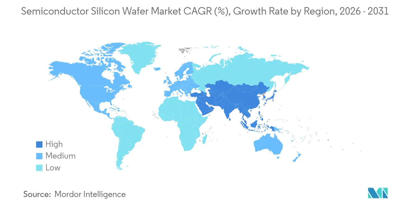
| Fastest Growing Market | Asia Pacific |
| Largest Market | Asia Pacific |
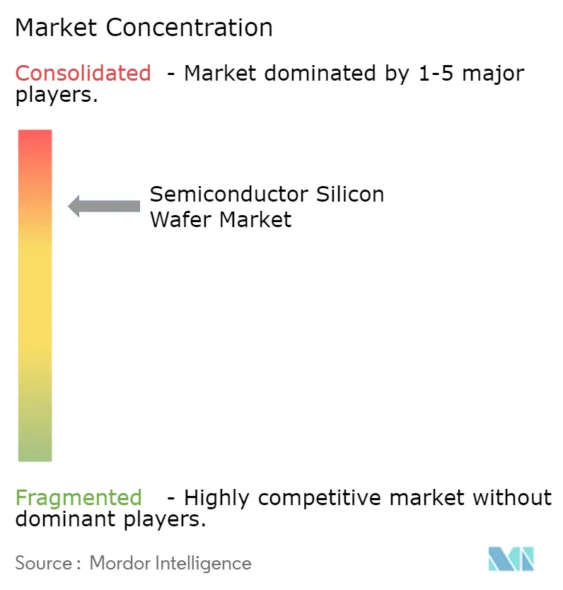
| Market Concentration | High |
Major Players *Disclaimer: Major Players sorted in no particular order Image © Mordor Intelligence. Reuse requires attribution under CC BY 4.0. | |
Semiconductor Silicon Wafer Market Analysis by Mordor Intelligence
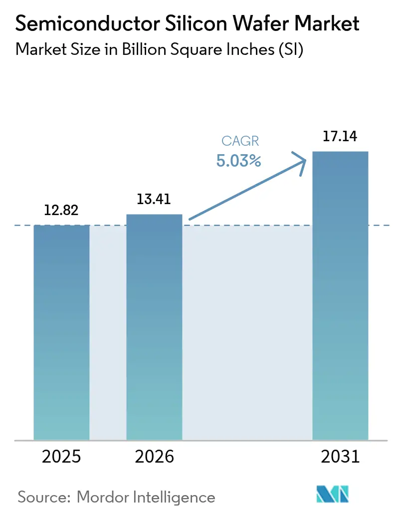
The semiconductor silicon wafer market size is projected to expand from 12.82 billion square inches in 2025, 13.41 billion square inches in 2026, to 17.14 billion square inches by 2031, registering a 5.03% CAGR over 2026-2031. Steady capacity additions at advanced logic foundries, sustained capital expenditures by memory makers, and policy-driven regional diversification are anchoring long-term demand. Equipment orders for 300 mm tools remain firm because extreme-ultraviolet nodes cannot be processed on smaller diameters, while mature-node devices continue to ride electrification and IoT tailwinds. Structural cost pressure on legacy fabs, coupled with the steep learning curve for ultra-flat substrates, protects incumbent suppliers even as Chinese newcomers lower prices on mature-grade wafers. Tightness in specialty 200 mm lines is lifting average selling prices, and automotive qualification requirements are lengthening contract horizons.
Key Report Takeaways
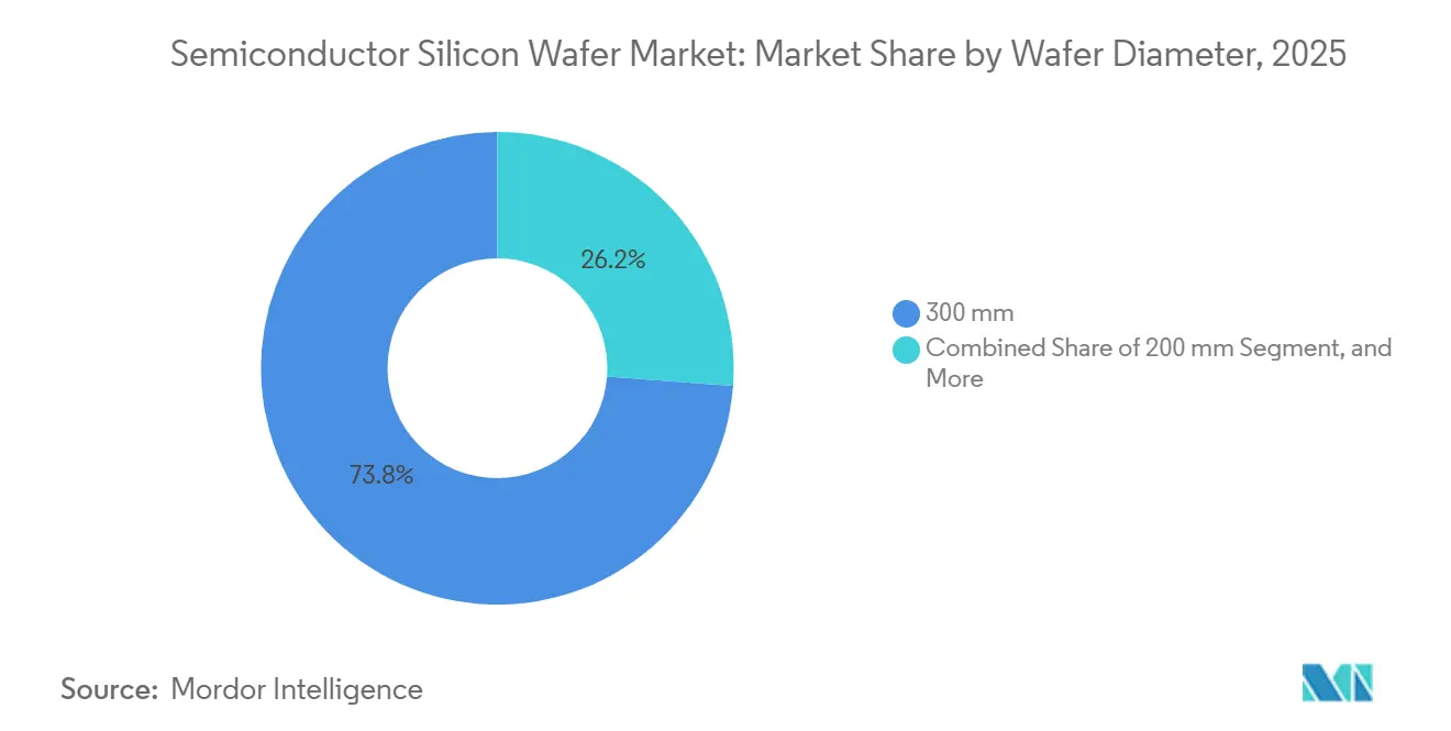
- By wafer diameter, 300 mm commanded 73.81% of 2025 volume, and the segment is advancing at a 5.18% CAGR through 2031.
- By semiconductor device type, discrete and power semiconductors held 14% of the semiconductor silicon wafer market share in 2025 and are forecast to grow at 6.22% CAGR to 2031.
- By technology node, advanced processes below 7 nm captured 24% of the 2025 semiconductor silicon wafer market size and are slated to post 7.04% CAGR during the forecast period.
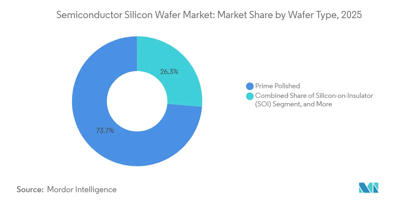
- By wafer type, prime polished substrates accounted for 73.66% of 2025 revenue, while silicon-on-insulator wafers are set to increase at a 5.42% rate to 2031.
- By end-user, automotive applications represented 8.31% of the 2025 semiconductor silicon wafer market size and will log the fastest 8.31% CAGR through 2031.
Note: Market size and forecast figures in this report are generated using Mordor Intelligence’s proprietary estimation framework, updated with the latest available data and insights as of 2026.
Global Semiconductor Silicon Wafer Market Trends and Insights
Drivers Impact Analysis*
| Driver | (~) % Impact on CAGR Forecast | Geographic Relevance | Impact Timeline |
|---|---|---|---|
| Rising Demand for 300 mm Wafers from Advanced Logic Fabs | +1.8% | Taiwan, South Korea, United States | Medium term (2-4 years) |
| Proliferation of 5G and IoT Consumer Devices | +1.2% | Asia-Pacific and North America | Short term (≤ 2 years) |
| Automotive-Grade Semiconductor Upswing (EVs and ADAS) | +1.5% | Europe, China, North America | Long term (≥ 4 years) |
| State-Subsidized Fab Build-Outs in China and Middle East | +0.9% | China, United Arab Emirates, Saudi Arabia | Medium term (2-4 years) |
| Specialty-Power 200 mm Line Tightness Elevating ASPs | +0.4% | Asia-Pacific and Europe | Short term (≤ 2 years) |
| Hybrid SOI and SiC-on-Si Substrates Expanding Silicon Area | +0.3% | Europe and North America | Long term (≥ 4 years) |
| Source: Mordor Intelligence | |||
Rising Demand for 300 mm Wafers From Advanced Logic Fabs
Advanced foundries now process every cutting-edge node on 300 mm equipment, as trip-gate and backside-power designs cannot run on smaller diameters. TSMC alone earmarked USD 52-56 billion of 2026 capital expenditure for 2 nm and 3 nm tools, while Samsung’s Taylor plant will install 50,000 wafers per month targeting 3 nm gate-all-around production in 2027.[1]Taiwan Semiconductor Manufacturing Company, “Quarterly Results and Capital Expenditure Guidance,” tsmc.com, Samsung Electronics, “Samsung Foundry Texas Fab Announcement 2024,” news.samsung.com Intel’s Arizona expansion, backed by USD 8.5 billion in CHIPS Act grants, adds 1.5 million 300 mm wafers monthly by 2028. Flatness requirements below 0.12 µm and total thickness variation under 0.30 µm exclude most new entrants, raising the moat around the five incumbent substrate makers. These locked-in volumes underpin a multiyear demand floor that persists even through cyclical downturns.
Proliferation of 5G and IoT Consumer Devices
Global 5G subscriptions climbed to 1.9 billion in 2025 as operators in China and the United States accelerated millimeter-wave deployments. RF-SOI wafers improve antenna-switch insertion loss by 0.3 dB, pushing Soitec’s order backlog to 18 months in early 2025.[2]Soitec, “Soitec Singapore RF-SOI Capacity Expansion Announcement,” soitec.com IoT endpoints consumed 800 million wafer-equivalent 200 mm substrates in 2025, up 12% year on year, as edge AI cameras and smart meters migrated to 40 nm mixed-signal flows. Bluetooth Low Energy 5.4 and Wi-Fi 7 chipsets entering mass production in 2026 keep mature-node fabs near full utilization, extending the life of 200 mm lines. Combined, consumer and IoT devices add steady, broad-based pull that cushions suppliers against memory downturns.
Automotive-Grade Semiconductor Upswing (EVs and ADAS)
Battery-electric vehicles reached 17% of global light-duty sales in 2025, each embedding 2,000-3,000 semiconductor devices versus 500 in combustion models. Silicon carbide modules moved to 200 mm wafers, with Wolfspeed and STMicroelectronics targeting 500,000 wafers annually by 2026.[3]Wolfspeed, “Wolfspeed 200 mm SiC Capacity Expansion Announcement,” wolfspeed.com Radar and camera processors remain on 28 nm and 40 nm, but must pass AEC-Q100 Grade 1, driving epitaxial wafer demand with doping uniformity below 2%.[4]Infineon Technologies, “Automotive Wafer Contracts Extended Through 2027,” infineon.com Automakers sign multiyear substrate contracts to guarantee supply, and tier-one suppliers pay 15-20% surcharges over 2024 levels to secure 200 mm capacity. Together, EV power and ADAS logic create the fastest-growing end-market for both 200 mm and 300 mm wafers.
State-Subsidized Fab Build-Outs in China and Middle East
China’s Ministry of Industry and Information Technology disbursed USD 70 billion in 2023-2025 subsidies that added 1.2 million 300 mm wafers per month of ingot capacity. The United Arab Emirates and Saudi Arabia pledged USD 10 billion for 200 mm specialty fabs aimed at automotive and industrial nodes.[5]Mubadala Investment Company, “Mubadala-GlobalFoundries UAE Fab Partnership Announcement,” mubadala.com These projects decouple regional wafer demand from traditional electronics cycles, but yield gaps of 10-15 percentage points versus Japanese peers slow penetration into advanced logic. Western device makers still prefer Japanese and European substrates to meet export-control compliance, effectively splitting the merchant market into dual supply chains. Nonetheless, subsidized capacity locks in incremental growth that lifts baseline global shipments.
Restraints Impact Analysis*
| Restraint | (~) % Impact on CAGR Forecast | Geographic Relevance | Impact Timeline |
|---|---|---|---|
| Ultra-Flat 300 mm Capex and Yield Challenges | -0.8% | Global entrants in China and Middle East | Medium term (2-4 years) |
| DRAM-Led Inventory Cycles Depressing Orders | -0.6% | South Korea and Taiwan | Short term (≤ 2 years) |
| Quartz Crucible and Polysilicon Purity Bottlenecks | -0.3% | Japan and China | Medium term (2-4 years) |
| SiC and GaN Material Substitution Risk | -0.2% | Early adopters in automotive and power | Long term (≥ 4 years) |
| Source: Mordor Intelligence | |||
Ultra-Flat 300 mm Capex and Yield Challenges
Building a modern 300 mm wafer plant costs more than USD 1 billion, and the 18-24 month learning curve pushes scrap rates to 30% before yields stabilize. Achieving total thickness variation below 0.30 µm requires tight control of crystal pulling, wire sawing, and chemical-mechanical polishing that only four or five firms have perfected over decades. Chinese suppliers lag incumbents by 10-15 yield points, restricting their access to 5 nm and 3 nm logic buyers. This steep entry barrier preserves the oligopoly and caps near-term supply elasticity despite state subsidies.
DRAM-Led Inventory Cycles Depressing Orders
Memory makers absorbed 28% of 300 mm wafer volume in 2025, yet they cut DRAM starts by 15% in late 2024 amid surplus inventory, driving a nine-month shipment dip for substrate vendors. Even as AI accelerators revived bit growth in early 2025, wafer orders lag device ramps by two to three quarters because contracts are locked six to nine months ahead. 3D NAND density gains also mean more bits per wafer, so fewer substrates cover the same storage growth.[6]Micron Technology, “3D NAND Layer Count Advances in 2025,” micron.com These swings inject ±5-7% volume volatility into annual shipments, complicating capacity planning for suppliers.
*Our forecasts treat driver/restraint impacts as directional, not additive. The impact forecasts reflect baseline growth, mix effects, and variable interactions.
Segment Analysis
By Wafer Diameter: Advanced Logic Keeps 300 mm on Top
The 300 mm category commanded 73.81% of wafer area in 2025, and this slice of the semiconductor silicon wafer market size is projected to expand at a 5.18% CAGR through 2031. Larger diameters let foundries amortize extreme-ultraviolet tool costs across more die, so every migration to 3 nm or 2 nm pulls incremental 300 mm volume. At the same time, 200 mm lines remain indispensable for power, analog, and mixed-signal chips that ship in high automotive and industrial grades, keeping utilization above 95%. Smaller 150 mm and 100 mm fabs survive on niche jobs, compound-semiconductor RF amps and sensor wafers, yet their combined share stays under 4%, underscoring an entrenched two-tier diameter landscape.
Capacity discipline explains the performance gap. Incumbent substrate makers prioritize ultra-flat 300 mm builds because premium pricing offsets the USD-billion capital outlay, whereas 200 mm expansions focus on specialty epitaxial or high-resistivity grades that lift margins without the same scale risks. As a result, foundries expect 80% of 300 mm output to feed advanced logic and HBM lines by 2031, while 200 mm retains its power-device stronghold. The widening bifurcation safeguards pricing for both diameters, ensuring balanced growth across mainstream and specialty flows.


By Semiconductor Device Type: Power Silicon Sets the Pace
Logic devices still led wafer consumption at 36.14% in 2025, but discrete and power semiconductors clock the fastest 6.22% compound growth as electrified vehicles and renewable energy systems multiply inverter counts. Silicon carbide and high-voltage insulated-gate bipolar transistors now rely on 200 mm substrates that boost throughput 40% versus 150 mm, sharpening volume demand. Memory, once the swing buyer, gradually surrenders share because each additional DRAM or NAND layer raises bits per wafer, diluting raw substrate needs even while bit shipments grow.
Analog gains ground too, as factory automation and vehicle sensor clusters require precision data converters on cost-optimized nodes. Optoelectronics, sensors, and MEMS, grouped at 8%, shift from 150 mm to 200 mm to cut scrap and standardize tooling. Together these moves rebalance the semiconductor silicon wafer market, tilting growth toward power and analog categories without upending logic’s headline leadership.
By Technology Node: Diverging Paths for Legacy and Leading Edge
Legacy geometries above 90 nm retained 40.57% of wafer area in 2025 because automotive controllers, connectivity transceivers, and cost-sensitive IoT chips value reliability over density. Mature nodes from 65 nm to 28 nm, holding 35%, strike a sweet spot for RF front-end and image-sensor integration, sustaining healthy orders for both 200 mm and 300 mm substrates. Advanced nodes below 7 nm captured 24% and will rise at a 7.04% pace as hyperscale cloud, artificial-intelligence accelerators, and flagship smartphones embrace 3 nm and 2 nm designs that only run on 300 mm equipment.
This three-way split tightens regional specialization. Advanced nodes concentrate in Taiwan, South Korea, and the United States, while China and the Middle East scale legacy and mature flows under state subsidy. The geographic divergence forces device makers to qualify multiple wafer sources, increasing switching costs and extending contract lengths, thereby giving suppliers better volume visibility across node classes.
By Wafer Type: SOI Moves from Niche to Necessity
Prime polished substrates dominated with 73.66% of 2025 revenue because bulk silicon still underpins mainstream logic, memory, and analog output. Epitaxial wafers at 16% stay critical for high-voltage devices and backside-illuminated image sensors that require controlled doping profiles. Silicon-on-insulator, though only 7% by volume, is expanding 5.42% yearly as 5G millimeter-wave handsets and automotive radar adopt fully-depleted architectures that slash parasitic capacitance.
Specialty high-resistivity and sensor-grade silicon fill the remaining 4% yet deliver outsized profitability thanks to purity and flatness specs that exceed 11-nines and sub-micron tolerances. The mix shift toward RF-SOI and ultra-high-resistivity grades diversifies revenue streams for wafer makers and cushions them against memory cyclicality, reinforcing the semiconductor silicon wafer market share held by incumbents.
By End-User Application: Vehicles Drive the Next Leg of Growth
Consumer electronics consumed 41.47% of wafer area in 2025 as smartphones, PCs, and wearables maintained steady refresh cycles, but automotive demand is racing ahead with an 8.31% CAGR. Each battery electric vehicle integrates up to 3,000 chips spanning traction inverters, battery management, and advanced driver-assistance processors, translating into 15-20 wafer equivalents per car. Industrial applications, at 18%, benefit from electrified factory floors and smart-grid rollouts that raise orders for power and sensing silicon.
Telecom infrastructure, holding 12%, moderates after initial 5 G rollouts, yet still banks replacement demand for higher-bandwidth remote radio heads. The rebalancing trims consumer’s slice toward 37% by 2031 even as absolute consumer-device shipments rise, underscoring how transportation and industrial electrification are redefining long-term substrate requirements across the semiconductor silicon wafer market.
Geography Analysis
Asia-Pacific dominated with 78.53% of 2025 wafer consumption and will post a 5.27% annual rise through 2031 as Taiwan’s foundry cluster and South Korea’s memory leaders keep expanding 300 mm footprints. Mainland China adds mature-node capacity at speed under a USD 70 billion subsidy push, yet yield gaps slow its penetration into sub-10 nm logic. Japan underwrites more than half of global substrate supply thanks to decades-old crystal-pulling know-how, and fresh investments in ultra-flat 300 mm lines aim to lock that lead until at least 2031.
North America held 12% of demand but gains momentum from the USD 52.7 billion CHIPS and Science Act. Intel’s Ohio and Arizona mega-fabs, TSMC’s Arizona campus, and GlobalWafers’ Texas plant collectively add over 2.7 million 300 mm wafers per month by 2028, although utilization ramps in stages. Canada and Mexico stay focused on assembly, test, and advanced packaging, complementing United States front-end expansions.
Europe captured 7%, with the European Chips Act funneling EUR 43 billion (USD 48 billion) into new capacity. The Dresden-based European Semiconductor Manufacturing Company targets 40,000 300 mm wafers per month for automotive microcontrollers by 2027, while Siltronic broadens ingot output under multiyear contracts. South America and the Middle East and Africa together make up 2.5%, yet Gulf state projects in Abu Dhabi and Riyadh position the region as an emerging hub for 130 nm-180 nm automotive and industrial flows, rounding out a more regionally balanced semiconductor silicon wafer market.
Mordor Intelligence provides coverage of the semiconductor silicon wafer market across other key regional markets, including Europe, North America, and Asia, each with their regulatory frameworks and demand patterns. Detailed country-level analysis extends to Germany, United States, Japan, South Korea, Taiwan, India, and China incorporating local coverage and market participation, as required.

Competitive Landscape
Five incumbent manufacturers, Shin-Etsu Chemical, SUMCO, GlobalWafers, Siltronic, and SK Siltron, controlled about 85% of global 300 mm capacity in 2025, reflecting multibillion-dollar capital barriers and proprietary crystal-pulling expertise. Shin-Etsu and SUMCO together delivered more than half of worldwide volume and invested JPY 150 billion (USD 1 billion) in 2025 to add 200,000 wafers per month of ultra-flat capacity for 2 nm and 3 nm nodes. GlobalWafers followed with a USD 5 billion Texas plant that reaches 1.2 million wafers annually by 2027, aimed at U.S. customers seeking secure supply.
Chinese challengers, National Silicon Industry Group, Shanghai Simgui Technology, and Zhonghuan Advanced Semiconductor Materials, focus on mature-grade wafers where flatness targets are looser, pricing 10-15% below Japanese peers to win share in domestic automotive and industrial fabs. Yield gaps, however, restrict them from 5 nm buyers, and Western export-control lists make it harder to serve multinational logic customers.
Vertical integration is expanding: Samsung Electronics and Intel both added internal crystal-pulling lines to insulate against merchant-market price swings, removing an estimated 3-5% of annual wafer demand from open trading. Specialty niches remain fragmented; Soitec dominates silicon-on-insulator with its Smart Cut technology and filed 18 patents in 2024-2025 to lower defect density below 0.05 cm², a threshold essential for fully depleted. Okmetic and Topsil split the float-zone market for ultra-high-resistivity substrates demanded by millimeter-wave switches, where resistivity above 1,000 Ω-cm cuts signal loss by 0.2 dB.
Regulatory requirements raise the bar further. ISO 26262 traceability rules for automotive-grade wafers force suppliers to log crystal orientation, oxygen content, and surface roughness at batch level, favoring firms with established quality management systems. Environmental, social, and governance audits from vehicle OEMs also promote long-term contracts, cementing the incumbents’ hold on high-specification segments even as regional subsidies bankroll new entrants.
Semiconductor Silicon Wafer Industry Leaders
Shin-Etsu Chemical Co., Ltd.
SUMCO Corporation
GlobalWafers Co., Ltd.
Siltronic AG
SK Siltron Co., Ltd.
- *Disclaimer: Major Players sorted in no particular order

Recent Industry Developments
- March 2026: TSMC Arizona Fab 21 Phase 1 began 4 nm production with 20,000 300 mm wafers per month capacity, backed by USD 6.6 billion in CHIPS funding.
- January 2026: Soitec opened its Singapore expansion, tripling RF-SOI output to 3 million 300 mm-equivalent wafers annually by 2027 under long-term deals with Qualcomm and MediaTek.
- December 2025: GlobalWafers completed phase-one build-out of its Sherman, Texas 300 mm facility, hitting 300,000 wafers per year initial run rate.
- November 2025: Shin-Etsu Chemical invested JPY 150 billion (USD 1 billion) to add 200,000 300 mm wafers per month at its Shirakawa and Takefu sites, targeting 2 nm and 3 nm nodes.


Global Semiconductor Silicon Wafer Market Report Scope
Silicon wafers are thin slices of pure or doped silicon cut from silicon ingots. Their thicknesses range from a few millimeters to a few microns and can be tuned according to the application through thinning processes. They are extensively used in smartphones, smartwatches, computers, tablets, gas sensors, and smart home sensors.
The Semiconductor Silicon Wafer Market Report is Segmented by Wafer Diameter (≤150mm, 200mm, 300mm), Semiconductor Device Type (Logic, Memory, Analog, Discrete/Power, Other), Technology Node (Advanced <7nm, Mature 28-65nm, Legacy >90nm), Wafer Type (Prime Polished, Epitaxial, SOI, Specialty), End-user (Consumer Electronics, Industrial, Telecommunications, Automotive, Other), and Geography (North America, Europe, Asia-Pacific, South America, Middle East and Africa). Market Forecasts are Provided in Terms of Shipments in Area (Billion Square Inches).
| ≤150mm |
| 200 mm |
| 300mm |
| Logic |
| Memory |
| Analog |
| Discrete/Power |
| Other Semiconductor Device Types (Optoelectronics, Sensors, Micro) |
| Advanced Node Wafer Market (<7nm including 5nm, 3nm, and 2nm) |
| Mature Node Wafer Market (28nm-65nm) |
| Legacy Node Wafer Market (>90nm) |
| Prime Polished |
| Epitaxial |
| Silicon-on-Insulator (SOI) |
| Specialty Silicon (High-Resistivity, Power, Sensor-Grade) |
| Consumer Electronics | Mobile and Smartphones |
| PCs and Servers | |
| Industrial | |
| Telecommunications | |
| Automotive | |
| Other End-user Applications |
| North America | United States |
| Canada | |
| Mexico | |
| Europe | Germany |
| United Kingdom | |
| France | |
| Rest of Europe | |
| Asia-Pacific | China |
| Japan | |
| India | |
| South Korea | |
| Taiwan | |
| Rest of Asia-Pacific | |
| South America | |
| Middle East and Africa |
| By Wafer Diameter | ≤150mm | |
| 200 mm | ||
| 300mm | ||
| By Semiconductor Device Type | Logic | |
| Memory | ||
| Analog | ||
| Discrete/Power | ||
| Other Semiconductor Device Types (Optoelectronics, Sensors, Micro) | ||
| By Technology Node | Advanced Node Wafer Market (<7nm including 5nm, 3nm, and 2nm) | |
| Mature Node Wafer Market (28nm-65nm) | ||
| Legacy Node Wafer Market (>90nm) | ||
| By Wafer Type | Prime Polished | |
| Epitaxial | ||
| Silicon-on-Insulator (SOI) | ||
| Specialty Silicon (High-Resistivity, Power, Sensor-Grade) | ||
| By End-user Application | Consumer Electronics | Mobile and Smartphones |
| PCs and Servers | ||
| Industrial | ||
| Telecommunications | ||
| Automotive | ||
| Other End-user Applications | ||
| By Geography | North America | United States |
| Canada | ||
| Mexico | ||
| Europe | Germany | |
| United Kingdom | ||
| France | ||
| Rest of Europe | ||
| Asia-Pacific | China | |
| Japan | ||
| India | ||
| South Korea | ||
| Taiwan | ||
| Rest of Asia-Pacific | ||
| South America | ||
| Middle East and Africa | ||


Key Questions Answered in the Report
What is the forecast size of the semiconductor silicon wafer market by 2031?
The market is expected to reach 17.14 billion square inches by 2031, reflecting a 5.03% CAGR over 2026-2031.
Which wafer diameter segment is growing fastest?
300 mm substrates are expanding at a 5.18% CAGR because every cutting-edge logic and memory node requires this diameter for cost and yield efficiency.
How will automotive demand influence future wafer consumption?
Electrified and automated vehicles will drive the fastest 8.31% growth, lifting demand for both 200 mm power wafers and 300 mm logic wafers qualified to strict automotive standards.
Which region will capture the largest share of new wafer capacity?
Asia-Pacific will maintain leadership with more than three-quarters of global consumption, supported by foundry and memory expansions in Taiwan, South Korea, and subsidy-backed growth in mainland China.
Who are the leading suppliers of silicon wafers?
Shin-Etsu Chemical, SUMCO, GlobalWafers, Siltronic, and SK Siltron collectively held almost one fourth or more of the market share of 300 mm capacity in 2025.
Page last updated on:


