| Study Period | 2019 - 2030 |
| Market Size (2025) | USD 25.61 Billion |
| Market Size (2030) | USD 36.94 Billion |
| CAGR (2025 - 2030) | 7.60 % |
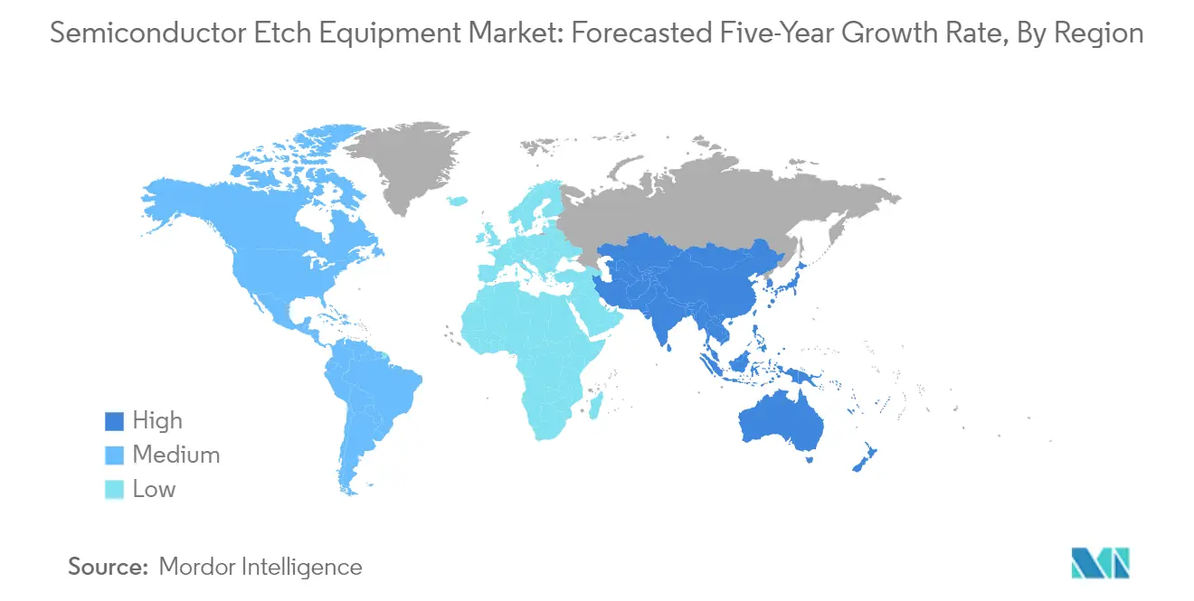
| Fastest Growing Market | Asia-Pacific |
| Largest Market | Asia-Pacific |
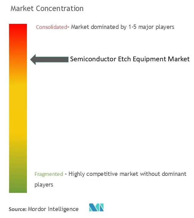
| Market Concentration | High |
Major Players*Disclaimer: Major Players sorted in no particular order |
.webp "Semiconductor Etch Equipment Market Major Players")

Semiconductor Etch Equipment Market Analysis
The Semiconductor Etch Equipment Market size is estimated at USD 25.61 billion in 2025, and is expected to reach USD 36.94 billion by 2030, at a CAGR of 7.6% during the forecast period (2025-2030).
The semiconductor equipment industry is experiencing unprecedented transformation driven by massive investments in manufacturing capacity expansion and technological advancement. Major industry players are aggressively expanding their production capabilities to address the growing demand for semiconductor devices. Intel's announcement of a EUR 88 billion investment across several European countries in March 2022 exemplifies this trend, demonstrating the industry's commitment to building robust manufacturing capabilities. These investments are particularly focused on developing advanced etching technologies capable of handling increasingly complex semiconductor architectures and smaller node sizes.
The integration of semiconductor processing equipment with emerging technologies is reshaping manufacturing capabilities and efficiency. The industry is witnessing a significant shift toward more sophisticated etching solutions that can support the development of advanced semiconductor devices for applications in artificial intelligence, the Internet of Things, and 5G technology. According to industry projections, 5G connections are expected to reach 1,100 million by 2025, covering approximately 34% of the world's population, which is driving the need for more advanced semiconductor fabrication equipment, including sophisticated etching solutions.
Supply chain resilience has become a central focus for the semiconductor equipment industry, with manufacturers implementing strategic initiatives to ensure consistent production capabilities. Companies are increasingly adopting localization strategies and establishing regional manufacturing hubs to minimize supply chain disruptions. For instance, Bosch's announcement to invest more than EUR 250 million by 2025 in expanding its wafer production facility in Reutlingen, Germany, demonstrates this shift toward strengthening regional manufacturing capabilities and reducing dependency on single-source suppliers.
The industry is witnessing a significant evolution in etching technologies to support the manufacturing of next-generation semiconductor devices. Advanced plasma etching systems are being developed to achieve higher precision and better control over the etching process, enabling the production of more complex semiconductor structures. This technological advancement is particularly evident in the development of new etching solutions for gate-all-around (GAA) transistor architectures and advanced memory devices, where precise material removal and pattern definition are crucial for device performance. Manufacturers are increasingly focusing on developing selective etching capabilities that can address the challenges of processing new materials and complex multi-layer structures while maintaining high throughput and yield.
Semiconductor Etch Equipment Market Trends
Increase in Capital Spending on Semiconductor Processing
The semiconductor industry is witnessing unprecedented levels of capital investment as manufacturers aim to address the growing demand for advanced chips across various applications. Major initiatives include Intel's massive USD 20 billion investment in new manufacturing sites in Columbus, Ohio, announced for developing and manufacturing advanced semiconductor chips, creating 3,000 permanent jobs on the 1,000-acre site. Similarly, China has demonstrated a strong commitment by working on a support package exceeding CNY 1 trillion (USD 143 billion) for its semiconductor industry, primarily allocated as subsidies and tax credits to strengthen semiconductor production and research activities. These investments reflect the industry's recognition of the critical role of advanced processing equipment, particularly semiconductor manufacturing equipment, in achieving higher production capabilities and technological advancement.
The surge in capital spending is further evidenced by Japan's strategic approach to semiconductor manufacturing, with the Ministry of Economy, Trade and Industry (METI) offering substantial subsidies worth up to JPY 476 billion (USD 3.5 billion) for semiconductor plants. This investment trend is complemented by Taiwan Semiconductor Manufacturing Co. (TSMC), Sony Group, and Denso's collaborative effort, with total investment reaching approximately USD 8.6 billion. The increasing adoption of smart devices and the integration of semiconductors in automotive, medical, aerospace, and various other sectors have created a strong demand for advanced chemical etching equipment, driving manufacturers to increase their capital expenditure on sophisticated processing technologies and equipment.
Understand The Key Trends Shaping This Market
Download PDF
Rapid Technological Advances and Transition
The semiconductor industry is experiencing rapid technological advancement, particularly in etching technologies required for producing increasingly complex and miniaturized semiconductor devices. Advanced etching systems, such as Applied Materials' Centris Sym3 Y, are being developed specifically for critical conductor etch applications in 3D NAND, DRAM, and foundry-logic nodes, enabling chipmakers to precisely pattern and shape ever-smaller features in state-of-the-art memory and logic chips. The industry's push toward more sophisticated technologies is evident in developments like Gate All Around (GAA) technology and 3D stacking technology, which require highly selective dry etch equipment to achieve the desired precision and performance in next-generation memory and system semiconductors.
The technological transition is further characterized by innovations in Metal Insulator Metal (MIM) capacitors and advanced packaging solutions, driving the need for more sophisticated wet etch equipment. Companies are investing in research and development to create new etching solutions that can handle the increasing complexity of semiconductor structures while maintaining high precision and reliability. For instance, Lam Research's introduction of new selective etch devices specifically designed for GAA technology and 3D stacking applications demonstrates the industry's commitment to advancing etching capabilities to meet the demands of next-generation semiconductor manufacturing processes. These technological advances are essential for supporting emerging applications in artificial intelligence, 5G communications, and Internet of Things (IoT) devices, which require increasingly sophisticated semiconductor components. The semiconductor equipment market is thus poised for significant growth, driven by these technological innovations and the increasing need for plasma etch equipment.
Segment Analysis: By Product Type
High-density Etch Equipment Segment in Semiconductor Etch Equipment Market
The high-density semiconductor etch equipment segment dominates the global semiconductor etch equipment market, commanding approximately 66% market share in 2024. This segment's prominence is driven by its crucial role in advanced semiconductor manufacturing processes, particularly in creating increasingly complex and miniaturized chip designs. The technology's ability to deliver precise pattern transfer and superior etch profiles makes it essential for manufacturing cutting-edge semiconductors used in 5G devices, artificial intelligence processors, and high-performance computing applications. The segment is also experiencing the fastest growth trajectory, with a projected growth rate of nearly 6% from 2024 to 2029, primarily due to increasing demand for high-precision etching in advanced node semiconductor fabrication and the continuous push toward smaller semiconductor geometries.

Low-density Etch Equipment Segment in Semiconductor Etch Equipment Market
The low-density wafer etching equipment segment maintains its significant position in the semiconductor etch equipment market, particularly in applications where cost-effectiveness and specific processing requirements are paramount. This segment serves crucial roles in various semiconductor manufacturing processes, especially in areas where high-energy reactions at lower energy costs are beneficial. The technology's ability to produce effective results with relatively small quantities of chemicals and electricity makes it particularly attractive for manufacturers looking to optimize operational costs while maintaining acceptable quality levels. The segment continues to find applications in automotive semiconductors, power devices, and other specialized applications where specific etching requirements align well with low-density plasma technology capabilities.
Segment Analysis: By Etching Film Type
Conductor Etching Segment in Semiconductor Etch Equipment Market
The conductor etching segment maintains its dominant position in the semiconductor etch equipment market, commanding approximately 44% market share in 2024. This segment's prominence is driven by its crucial role in shaping the electrically active materials used in different parts of semiconductor devices. The increasing demand for miniaturization in semiconductor circuits and the growing complexity of modern chip designs have further cemented the segment's leadership position. Conductor etching equipment is particularly vital in applications requiring precise control over electrical interconnections, with even minimal variations potentially leading to electrical faults impacting device performance. The segment's growth is also supported by the rising adoption of advanced packaging technologies and the increasing integration of semiconductors in automotive and consumer electronics applications.
Polysilicon Etching Segment in Semiconductor Etch Equipment Market
The polysilicon etching segment is emerging as the fastest-growing segment in the semiconductor etch equipment market, with an expected growth rate of approximately 5% during 2024-2029. This robust growth is primarily driven by the increasing adoption of polysilicon in various applications, including gate electrodes, interconnects for metal oxide semiconductor circuits, and floating gates for memory cells. The segment's growth is further accelerated by the rising demand for high-performance memory systems and the increasing complexity of semiconductor memory IP. The development of new etching technologies and processes specifically optimized for polysilicon applications is also contributing to the segment's rapid expansion, particularly in advanced node manufacturing processes.
Remaining Segments in Etching Film Type Market
The dielectric etching segment plays a vital role in the semiconductor etch equipment market by focusing on the removal of non-conductive materials during device manufacturing. This segment is particularly crucial in the fabrication of advanced memory devices with challenging structures, such as deep holes and trenches that require precise manufacturing tolerances. The segment's importance is amplified by the growing demand for high-performance computing devices and the increasing complexity of semiconductor architectures. Dielectric etching continues to evolve with the introduction of new materials and processes, particularly in applications requiring tight critical dimension control and stable processing capabilities.
Segment Analysis: By Application
Foundries Segment in Semiconductor Etch Equipment Market
The foundries segment dominates the semiconductor etch equipment market, driven by massive investments in new fabrication facilities and capacity expansion globally. Major semiconductor manufacturers are significantly increasing their foundry investments to address the growing demand for chips across various applications, including artificial intelligence, 5G networks, and advanced computing systems. The segment's prominence is further reinforced by government initiatives worldwide to boost domestic semiconductor manufacturing capabilities, particularly in regions like the United States, Europe, and Asia. Leading foundries are implementing advanced etching technologies to achieve higher precision and efficiency in chip manufacturing, especially for nodes below 7 nanometers. The increasing complexity of semiconductor devices and the need for more sophisticated etching processes in modern foundries continue to drive innovation in etch equipment technology. Additionally, the focus on developing specialized foundry capabilities for emerging applications like automotive semiconductors and high-performance computing is further strengthening this segment's market position.
MEMS Segment in Semiconductor Etch Equipment Market
The MEMS (Micro-electromechanical systems) segment is experiencing rapid growth in the semiconductor etch equipment market, driven by expanding applications across multiple industries. The segment's growth is propelled by increasing adoption of MEMS devices in automotive systems, consumer electronics, medical devices, and Industrial IoT applications. The demand for more sophisticated MEMS manufacturing processes is driving investments in advanced etching equipment that can handle complex three-dimensional structures with high precision. The integration of MEMS technology in emerging applications such as autonomous vehicles, smart devices, and biomedical implants is creating new opportunities for etch equipment manufacturers. The segment is witnessing significant technological advancements in etching processes to achieve better control over feature sizes and improved yield rates. Furthermore, the growing trend toward miniaturization and increased functionality in electronic devices is pushing the boundaries of MEMS fabrication, requiring more advanced etching solutions. The development of new MEMS applications in 5G infrastructure and edge computing devices is also contributing to the segment's robust growth trajectory.
Remaining Segments in Application Market Segmentation
The sensors and power devices segments also play crucial roles in shaping the semiconductor etch equipment market landscape. The sensors segment is driven by the proliferation of IoT devices and increasing implementation of sensor technology in smart manufacturing, automotive applications, and consumer electronics. The demand for more sophisticated and precise sensors is pushing the boundaries of etching technology capabilities. Meanwhile, the power devices segment is gaining prominence due to the growing focus on energy efficiency and the electrification trend in the automotive industry. This segment requires specialized etching solutions for handling wide-bandgap semiconductors and other advanced materials used in power electronics. Both segments are benefiting from ongoing technological advancements in etching processes and the industry's push toward more efficient and precise semiconductor manufacturing capabilities.
Semiconductor Etch Equipment Market Geography Segment Analysis
Semiconductor Etch Equipment Market in North America
The North American semiconductor etch equipment market continues to be driven by significant technological advancements and robust manufacturing capabilities, holding approximately 10% of the global market share in 2024. The region's market is characterized by the presence of leading semiconductor equipment manufacturers and extensive research and development activities in semiconductor fabrication equipment. The United States remains at the forefront of innovation in semiconductor processing equipment, particularly in developing new chip products like GPUs and microprocessors. The region's strength lies in its advanced manufacturing infrastructure, highly skilled workforce, and strong intellectual property protection framework. Major semiconductor manufacturers are focusing on expanding their production capabilities through state-of-the-art facilities equipped with advanced etching technologies. The emphasis on domestic semiconductor manufacturing capabilities has been reinforced by recent government initiatives and investments in the sector. Additionally, the growing demand for semiconductors in emerging technologies such as artificial intelligence, 5G networks, and autonomous vehicles continues to drive market growth in the region.
Semiconductor Etch Equipment Market in Europe
The European semiconductor etch equipment market has demonstrated remarkable growth, experiencing an increase of approximately 69% from 2019 to 2024. The region's market is characterized by a strong focus on automotive and industrial applications, particularly in countries like Germany, France, and the Netherlands. European manufacturers are increasingly investing in advanced semiconductor manufacturing equipment to reduce dependence on external suppliers and strengthen domestic production capabilities. The market is witnessing significant developments in specialized etching technologies for power semiconductors and automotive chips. The region's strong research and development infrastructure, coupled with collaboration between academic institutions and industry players, continues to drive innovation in etching technologies. European semiconductor manufacturers are particularly focused on developing sustainable and energy-efficient etching processes, aligning with the region's strong environmental regulations and sustainability goals. The market is also benefiting from increased investments in digital infrastructure and the growing adoption of Industry 4.0 technologies.
Semiconductor Etch Equipment Market in Asia Pacific
The Asia Pacific region dominates the global semiconductor etch equipment market, with a projected growth rate of approximately 5% during 2024-2029. The region serves as the global hub for semiconductor manufacturing, with countries like Taiwan, South Korea, Japan, and China leading in advanced semiconductor fabrication capabilities. The market is characterized by extensive manufacturing infrastructure, competitive cost structures, and strong government support for semiconductor industry development. Major foundries in the region are continuously upgrading their facilities with advanced etching equipment to maintain technological leadership in semiconductor manufacturing. The region's market is driven by the presence of leading semiconductor manufacturers, robust supply chain networks, and increasing domestic demand for electronic devices. The integration of advanced technologies in manufacturing processes, coupled with rising investments in research and development, continues to strengthen the region's position in the global semiconductor industry. The market is also benefiting from the growing adoption of advanced packaging technologies and the increasing demand for high-performance computing devices.
Semiconductor Etch Equipment Market in Rest of the World
The Rest of the World region, comprising Latin America, the Middle East, and Africa, represents an emerging market for semiconductor etch equipment with growing potential. While the current market presence is relatively limited, these regions are witnessing increasing investments in electronics manufacturing and semiconductor capabilities. The market is primarily driven by growing industrialization, increasing adoption of digital technologies, and government initiatives to develop local manufacturing capabilities. Countries in these regions are focusing on developing their technological infrastructure and attracting investments in semiconductor manufacturing. The automotive and consumer electronics sectors are emerging as key drivers for semiconductor demand in these regions. Local governments are implementing favorable policies and incentives to attract semiconductor manufacturers and develop domestic production capabilities. The market is also benefiting from increasing investments in telecommunications infrastructure and the growing adoption of smart devices. These regions present significant growth opportunities as they continue to develop their technological capabilities and manufacturing infrastructure.
Get Analysis on Important Geographic Markets
Download PDF
Semiconductor Etch Equipment Industry Overview
Top Companies in Semiconductor Etch Equipment Market
The semiconductor etch equipment market is dominated by established players like Applied Materials, Lam Research, Tokyo Electron, Hitachi High-Tech, and ULVAC, who have built a strong global presence through decades of innovation and customer relationships. These companies are heavily investing in research and development to advance their etching technologies, particularly focusing on solutions for next-generation semiconductor manufacturing equipment processes, including advanced packaging and 3D structures. The industry witnesses continuous product launches targeting enhanced precision, improved throughput, and reduced environmental impact. Companies are expanding their manufacturing footprint, especially in Asia-Pacific, to be closer to key customers and strengthen supply chain resilience. Strategic collaborations with research institutions, universities, and semiconductor manufacturers have become crucial for co-developing cutting-edge solutions. Market leaders are also diversifying their product portfolios through acquisitions and partnerships to offer comprehensive semiconductor equipment solutions.
High Barriers Shape Competitive Market Dynamics
The semiconductor equipment industry exhibits a relatively consolidated structure dominated by large global players who possess extensive technological capabilities and established relationships with major semiconductor manufacturers. These companies have built formidable barriers to entry through their substantial investments in research and development, advanced manufacturing capabilities, and comprehensive service networks. The market has witnessed strategic consolidation through mergers and acquisitions, as established players seek to enhance their technological capabilities and expand their geographic presence. Companies are increasingly focusing on vertical integration to maintain better control over their supply chains and ensure consistent quality standards.
The competitive landscape is characterized by intense rivalry among established players, with competition primarily centered on technological innovation, product performance, and customer support capabilities. Market leaders have established strong footholds in key semiconductor manufacturing regions, particularly in Asia-Pacific, where they maintain close relationships with major foundries and integrated device manufacturers. The industry's high capital requirements and complex technological demands make it challenging for new entrants to establish a significant presence, leading to a market structure where established players continue to strengthen their positions through strategic investments and partnerships.
Innovation and Adaptability Drive Future Success
Success in the semiconductor etch equipment market increasingly depends on companies' ability to anticipate and address evolving customer needs while maintaining technological leadership. Market players must continuously invest in research and development to develop solutions for emerging applications such as artificial intelligence, 5G, and Internet of Things devices. Companies need to establish strong partnerships with semiconductor manufacturers early in their technology development cycles to ensure their equipment meets future manufacturing requirements. The ability to provide comprehensive support services and maintain a global presence has become crucial for capturing market share.
Future market success will require companies to balance innovation with operational efficiency while addressing growing environmental concerns and regulatory requirements. Players must develop more energy-efficient and environmentally friendly etching solutions while maintaining high performance standards. The increasing complexity of semiconductor devices and the need for more precise and reliable etching processes create opportunities for companies that can deliver superior technical solutions. Market participants must also maintain flexibility in their manufacturing and supply chain operations to address regional market variations and potential geopolitical challenges that could impact semiconductor manufacturing locations. Additionally, the integration of semiconductor cleaning equipment into their offerings can further enhance their market competitiveness.
Semiconductor Etch Equipment Market Leaders
-
Applied Materials Inc.
-
Hitachi High Technologies America, Inc.
-
Lam Research Corporation
-
Tokyo Electron Limited
-
Plasma-Therm LLC
- *Disclaimer: Major Players sorted in no particular order
Need More Details on Market Players and Competiters?
Download PDF
Semiconductor Etch Equipment Market News
- August 2024 - OKI Circuit Technology has launched an ultra-high-multilayer PCB line at its Joetsu Plant, Niigata Prefecture, started operations in July. The new line, enhancing production capacity by 1.4 times, supports semiconductor manufacturing and testing for AI, data centers, and next-gen communication networks. It features high-precision circuit formation with a via pitch of 0.23 mm and improved line width accuracy. The AOI automated inspection equipment has been relocated to optimize production flow and quality.
- April 2023 - Hitachi High-Tech Corporation announced that it would construct a new production facility in the Kasado Area of Kudamatsu City, Yamaguchi Prefecture, with an aim to increase the production capacity of etching systems for its semiconductor manufacturing equipment business, with production scheduled to begin in FY2025.
Semiconductor Etch Equipment Market Report - Table of Contents
1. INTRODUCTION
- 1.1 Study Assumptions and Market Definition
- 1.2 Scope of the Study
2. RESEARCH METHODOLOGY
3. EXECUTIVE SUMMARY
4. MARKET INSIGHTS
- 4.1 Market Overview
-
4.2 Industry Attractiveness - Porter's Five Forces Analysis
- 4.2.1 Bargaining Power of Suppliers
- 4.2.2 Bargaining Power of Buyers
- 4.2.3 Threat of New Entrants
- 4.2.4 Threat of Substitute Products
- 4.2.5 Intensity of Competitive Rivalry
- 4.3 Assessment of the Impact of COVID-19 on the Market
5. MARKET DYNAMICS
-
5.1 Market Drivers
- 5.1.1 Increase in Capital Spending on Semiconductor Processing
- 5.1.2 Rapid Technological Advances and Transition
-
5.2 Market Restraints
- 5.2.1 Trade Uncertainties and Semiconductor Memory Markets
6. MARKET SEGMENTATION
-
6.1 By Product Type
- 6.1.1 High-density Etch Equipment
- 6.1.2 Low-density Etch Equipment
-
6.2 By Etching Film Type
- 6.2.1 Conductor Etching
- 6.2.2 Dielectric Etching
- 6.2.3 Polysilicon Etching
-
6.3 By Application
- 6.3.1 Foundries
- 6.3.2 MEMS
- 6.3.3 Sensors
- 6.3.4 Power Devices
-
6.4 By Geography***
- 6.4.1 North America
- 6.4.2 Europe
- 6.4.3 Asia
- 6.4.4 Australia and New Zealand
- 6.4.5 Latin America
- 6.4.6 Middle East and Africa
7. COMPETITIVE LANDSCAPE
-
7.1 Company Profiles*
- 7.1.1 Applied Materials Inc.
- 7.1.2 Hitachi High Technologies America, Inc.
- 7.1.3 Lam Research Corporation
- 7.1.4 Tokyo Electron Limited
- 7.1.5 Plasma-Therm LLC
- 7.1.6 Panasonic Corporation
- 7.1.7 SPTS Technologies Limited (Orbotech)
- 7.1.8 Suzhou Delphi Laser Co., Ltd
- 7.1.9 ULVAC Inc.
8. INVESTMENT ANALYSIS
9. MARKET OPPORTUNITIES AND FUTURE TRENDS
**Subject to Availability
*** In the Final Report Asia, Australia and New Zealand will be Studied Together as 'Asia Pacific'
You Can Purchase Parts Of This Report. Check Out Prices For Specific Sections
Get Price Break-up Now
Semiconductor Etch Equipment Industry Segmentation
Semiconductor etch equipment is a device used to remove selective materials from the surface of the silicon wafer substrate by using various chemicals. The etching process removes the material from the surface of the semiconductor to create patterns according to its applications. It is being used in the semiconductor device fabrication process.
The Semiconductor Etch Equipment Market is segmented by product type (high-density etch equipment and low-density etch equipment), by etching film type (conductor etching, dielectric etching, and polysilicon etching), by application (foundries, MEMS, sensors, and power devices), and by geography (North America, Europe, Asia-Pacific, and the Rest of the World). The report offers the market size in value terms in USD for all the abovementioned segments.
| By Product Type | High-density Etch Equipment |
| Low-density Etch Equipment | |
| By Etching Film Type | Conductor Etching |
| Dielectric Etching | |
| Polysilicon Etching | |
| By Application | Foundries |
| MEMS | |
| Sensors | |
| Power Devices | |
| By Geography*** | North America |
| Europe | |
| Asia | |
| Australia and New Zealand | |
| Latin America | |
| Middle East and Africa |
Need A Different Region or Segment?
Customize Now
Semiconductor Etch Equipment Market Research FAQs
How big is the Semiconductor Etch Equipment Market?
The Semiconductor Etch Equipment Market size is expected to reach USD 25.61 billion in 2025 and grow at a CAGR of 7.60% to reach USD 36.94 billion by 2030.
What is the current Semiconductor Etch Equipment Market size?
In 2025, the Semiconductor Etch Equipment Market size is expected to reach USD 25.61 billion.
Who are the key players in Semiconductor Etch Equipment Market?
Applied Materials Inc., Hitachi High Technologies America, Inc., Lam Research Corporation, Tokyo Electron Limited and Plasma-Therm LLC are the major companies operating in the Semiconductor Etch Equipment Market.
Which is the fastest growing region in Semiconductor Etch Equipment Market?
Asia-Pacific is estimated to grow at the highest CAGR over the forecast period (2025-2030).
Which region has the biggest share in Semiconductor Etch Equipment Market?
In 2025, the Asia-Pacific accounts for the largest market share in Semiconductor Etch Equipment Market.
What years does this Semiconductor Etch Equipment Market cover, and what was the market size in 2024?
In 2024, the Semiconductor Etch Equipment Market size was estimated at USD 23.66 billion. The report covers the Semiconductor Etch Equipment Market historical market size for years: 2019, 2020, 2021, 2022, 2023 and 2024. The report also forecasts the Semiconductor Etch Equipment Market size for years: 2025, 2026, 2027, 2028, 2029 and 2030.
Our Best Selling Reports
Semiconductor Etch Equipment Market Research
Mordor Intelligence offers a comprehensive analysis of the semiconductor equipment industry. With decades of expertise in semiconductor manufacturing equipment research, we provide a detailed examination of the entire spectrum of semiconductor processing equipment. This includes chemical etching equipment, plasma etch equipment, and advanced semiconductor fabrication equipment. The report, available as an easy-to-download PDF, delivers in-depth insights into semiconductor cleaning equipment technologies and innovations in wafer processing equipment.
Stakeholders gain valuable insights into various etching technologies. These include deep reactive ion etch, wet etch equipment, and dry etch equipment applications. The analysis covers the entire semiconductor equipment ecosystem, from basic wafer etching equipment to sophisticated plasma processing equipment. Our research methodology ensures thorough coverage of semiconductor etch equipment developments and emerging trends in the semiconductor manufacturing equipment market. This provides actionable intelligence for industry decision-makers.