Semiconductor Bonding Equipment Market Size and Share
Market Overview
| Study Period | 2020 - 2031 |
|---|---|
| Market Size (2026) | USD 596.47 Million |
| Market Size (2031) | USD 755.32 Million |
| Growth Rate (2026 - 2031) | 4.84% CAGR |
| Fastest Growing Market | Asia Pacific |
| Largest Market | Asia Pacific |
| Market Concentration | Medium |
Major Players *Disclaimer: Major Players sorted in no particular order Image © Mordor Intelligence. Reuse requires attribution under CC BY 4.0. | |
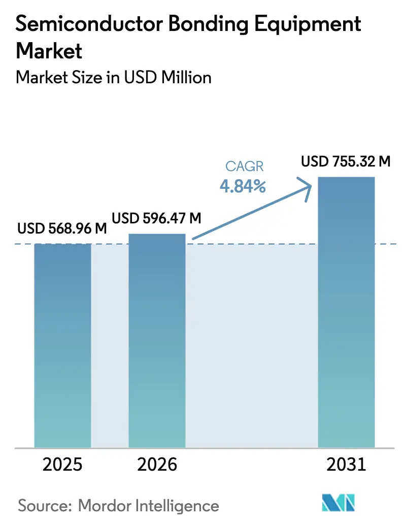
Semiconductor Bonding Equipment Market Analysis by Mordor Intelligence
The semiconductor bonding equipment market size in 2026 is estimated at USD 596.47 million, growing from 2025 value of USD 568.96 million with 2031 projections showing USD 755.32 million, growing at 4.84% CAGR over 2026-2031. Demand growth mirrors the industry shift from planar scaling to vertical stacking, where heterogeneous integration strategies require precise wafer-to-wafer and die-to-wafer connections. Leading chipmakers have accelerated capital spending on advanced packaging lines to improve bandwidth, latency, and energy efficiency for AI accelerators and high-performance computing devices. Hybrid copper-to-copper processes are eclipsing conventional wire bonding as sub-3 nm nodes move into risk production, raising alignment-accuracy demands below 10 µm. At the same time, automotive electrification and IoT miniaturization widen the application footprint, expanding order books for permanent, temporary, and hybrid platforms. However, the high total cost of ownership and tighter environmental rules on volatile organic compounds add pressure to sustain utilization levels above 70%, prompting buyers to negotiate full-service contracts and predictive-maintenance packages.
Key Report Takeaways
- By equipment type, permanent bonding equipment held the largest 38.74% of the semiconductor bonding equipment market share in 2025, while hybrid bonding systems are projected to grow at a 5.88% CAGR to 2031.
- By application, advanced packaging captured a 35.42% share of the semiconductor bonding equipment market in 2025; silicon photonics is forecast to expand at a 5.73% CAGR by 2031.
- By bonding technology, thermocompression led with 40.92% share of the semiconductor bonding equipment market size in 2025, and hybrid technology is advancing at a 6.07% CAGR through 2031.
- By wafer size, 200-300 mm represented 54.12% of the semiconductor bonding equipment market size in 2025; the >300 mm category is set to climb at 6.44% CAGR to 2031.
- By end-user, integrated device manufacturers represented 45.66% of the semiconductor bonding equipment market size in 2025; the foundries end-user is set to climb at 6.32% CAGR to 2031.
- By geography, Asia-Pacific represented 52.64% of the semiconductor bonding equipment market size in 2025; the segment is set to climb at 5.61% CAGR to 2031.
Note: Market size and forecast figures in this report are generated using Mordor Intelligence’s proprietary estimation framework, updated with the latest available data and insights as of 2026.
Global Semiconductor Bonding Equipment Market Trends and Insights
Drivers Impact Analysis*
| Driver | (~) % Impact on CAGR Forecast | Geographic Relevance | Impact Timeline |
|---|---|---|---|
| Increasing CAPEX by IDMs and foundries | +1.2% | Global, concentrated in APAC | Medium term (2-4 years) |
| Surging semiconductor content in automotive and IoT devices | +0.9% | Global, with early gains in Europe, North America | Long term (≥ 4 years) |
| Rapid adoption of advanced 2.5D/3D packaging platforms | +1.1% | APAC core, spill-over to North America | Medium term (2-4 years) |
| Government-backed "CHIPS" subsidies and tax incentives | +0.8% | North America and EU, with selective APAC programs | Short term (≤ 2 years) |
| Commercial roll-out of hybrid wafer-to-wafer bonding in CIS and 3D-NAND | +0.7% | APAC dominance, expanding to North America | Medium term (2-4 years) |
| Silicon-photonic interposers for AI datacenters driving wafer bonding tools | +0.6% | North America and EU, with APAC manufacturing | Long term (≥ 4 years) |
| Source: Mordor Intelligence | |||


Increasing CAPEX by IDMs and Foundries
Global semiconductor equipment spending hit USD 110 billion in 2024 and is on track for USD 130 billion by 2026.[1]SEMI, “2024 Equipment Spending by Region,” semi.org TSMC alone earmarked USD 38-42 billion for 2025 facility upgrades, a substantial portion of which funds advanced packaging and bonding lines.[2]Taiwan Semiconductor Manufacturing Co., “2025 CAPEX Guidance,” tsmc.com Comparable expansions by Samsung and Intel emphasize the competitive need for wafer-level integration that supports high-bandwidth memory and chiplet designs. Capital allocation now targets line items such as sub-micrometer optical alignment modules, vacuum bond chambers, and AI-enabled process control. Vendors that provide modular upgrade paths are gaining preferred-supplier status as device makers hedge against future design pivots. The investment uptick stimulates the semiconductor bonding equipment market by shortening replacement cycles and broadening the installed base across both front-end and back-end fabs.
Surging Semiconductor Content in Automotive and IoT Devices
Average semiconductor value per vehicle climbed to USD 950 in 2024, driven by electrified powertrains, advanced driver-assistance systems, and zonal architectures.[3]Bosch, “Semiconductor Content in Electric Vehicles,” bosch.com Electric models specify silicon-carbide and gallium-nitride power devices that need high-force, high-temperature bonding heads and robust flux-management systems. In parallel, IoT wearables and smart home nodes demand wafer-level chip-scale packages that shrink footprint and extend battery life. These divergent requirements converge at the equipment level, where configurable bonders must toggle between high-power pressure profiles and delicate MEMS handling. Suppliers are addressing the gap with adaptive clamp designs, real-time chuck-planarity feedback, and recipe-driven force curves. The trend raises unit shipments in the semiconductor bonding equipment market while diversifying revenue streams across automotive Tier-1s and consumer OEMs.
Rapid Adoption of Advanced 2.5D/3D Packaging Platforms
Shipments of 2.5D interposers rose 35% year over year in 2024 as HPC processors adopted chiplet architectures for die-to-die interconnect flexibility.[4]Applied Materials, “Hybrid Bonding in Advanced Packaging,” appliedmaterials.com Three-dimensional stacking pushes throughput-first bonders to achieve placement repeatability below 500 nm while containing warp on thinned wafers. Equipment makers now bundle thermal-modeling software and in-situ metrology to pre-correct distortion during compression cycles. Reliability validation, once a downstream test-house function, moves upstream into the bonding tool with embedded acoustic imaging. As front-end and back-end workflows merge, purchasing departments renegotiate service agreements to cover the hybrid process window, reinforcing demand momentum for comprehensive platforms in the semiconductor bonding equipment market.
Government-Backed “CHIPS” Subsidies and Tax Incentives
The U.S. CHIPS and Science Act allocates USD 52.7 billion, including sizeable grants reserved for advanced packaging lines. Texas Instruments, for instance, secured USD 1.6 billion to expand domestic assembly facilities focused on wafer-to-wafer bonding of analog and power devices. Europe mirrors the effort with an EUR 43 billion package that guides member states toward packaging self-sufficiency. Early awardees are leveraging funds to offset the capital premium of vacuum bonders and temperature-controlled cleanrooms. While subsidies accelerate orders in the semiconductor bonding equipment market, vendors remain cautious about cliff-edge risks once funding sunsets.
Restraints Impact Analysis*
| Restraint | (~) % Impact on CAGR Forecast | Geographic Relevance | Impact Timeline |
|---|---|---|---|
| High cost of ownership and TCO uncertainty | -0.7% | Global, particularly acute in emerging markets | Short term (≤ 2 years) |
| Process complexity at sub-10 µm alignment tolerances | -0.5% | Global, concentrated in advanced node facilities | Medium term (2-4 years) |
| Supply-chain bottlenecks for ultra-flat carrier wafers | -0.4% | Global, with APAC supply concentration | Short term (≤ 2 years) |
| Stricter VOC / adhesive-chemistry environmental regulations | -0.3% | EU and North America leading, APAC following | Long term (≥ 4 years) |
| Source: Mordor Intelligence | |||
High Cost of Ownership and TCO Uncertainty
State-of-the-art hybrid bonders list above USD 3 million, while annual running costs including spares, consumables, and calibration can lift lifetime spend to USD 8 million. Smaller OSATs struggle when utilization drifts below 70%, especially in consumer-electronics off-seasons. Rapid roadmap updates further complicate financial modeling because a tool qualified for 10 µm overlay may need retrofit kits after only two product cycles. Leasing programs, outcome-based service contracts, and shared-risk pricing models are emerging, yet CFOs still cite uncertain residual value as a brake on new orders within the semiconductor bonding equipment market.
Process Complexity at Sub-10 µm Alignment Tolerances
Bringing overlay error down to single-digit micrometers forces fabs to enforce temperature stability within ±0.1 °C and implement active vibration isolation on the sub-nanometer scale. Process engineers spend extra quarters refining bond recipes, extending time-to-money for greenfield lines. Even mature fabs must recalibrate inspection metrology, edge-bead removal, and plasma-clean steps to curb void defects. Training requirements intensify as operators shift from mechanical adjustments to software-defined offsets guided by real-time machine-vision feedback. The heightened complexity contributes to lengthier qualification and validation cycles, tempering roll-out speed in the semiconductor bonding equipment market.
*Our forecasts treat driver/restraint impacts as directional, not additive. The impact forecasts reflect baseline growth, mix effects, and variable interactions.
Segment Analysis
By Equipment Type: Hybrid Platforms Gain Ground
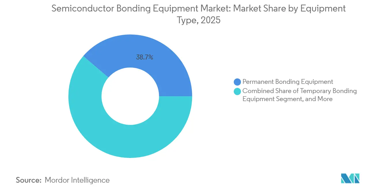
Permanent bonders accounted for 38.74% of 2025 revenue, underpinned by their proven reliability in legacy device packaging. Temporary bonding tools cater to wafer thinning and TSV creation, providing the reversible adhesion needed for mechanical support. Hybrid systems register the quickest climb at 5.88% CAGR, targeting sub-3 nm integration where copper-to-copper direct attach minimizes resistance and electromigration. That growth lifts the semiconductor bonding equipment market size for hybrid platforms from a modest base toward parity with permanent tools before the decade closes. Manufacturers differentiate through dual-stage alignment optics, active levelling chucks, and closed-loop pressure control that collectively push placement error below 500 nm. Buyers favor multi-modal units that accept future recipe add-ons, lowering capital risk. The pivot intensifies R&D around heat-spreader materials and compliant under-fill chemistries that withstand repeated thermal cycles without delamination. Competition also hinges on throughput, with flagship machines now promising 20% cycle-time reductions achieved via parallel clamp arms and predictive servo tuning.
A broader equipment refresh cycle accompanies the shift. Line managers audited older eutectic stations and discovered maintenance outlays rising 12% per year. Swapping to hybrid bonders eliminates dual-pass processes, improving floor utilization. Yet stakeholders insist that new gear integrate seamlessly with MES and factory automation layers that handle traceability down to die serial number. Vendors respond by embedding OPC-UA gateways and edge analytics that channel process data into AI-based yield dashboards. Such ecosystem compatibility accelerates factory-wide adoption, reinforcing the hybrid segment’s contribution to the semiconductor bonding equipment market.


By Application: Silicon Photonics Takes Off
Advanced packaging maintained 35.42% of 2025 revenue and remains the anchor segment, buttressed by chiplet processors, high-bandwidth memory, and premium smartphone SoC programs. Power IC bonding, while less glamorous, delivers stable volumes that depend on rigorous void-control protocols and high-pressure thermocompression heads. Silicon photonics is the standout high-velocity niche at a 5.73% CAGR. Optical engines co-packaged with switch ASICs need micron-accurate placement of germanium photodetectors and III-V lasers onto silicon carrier wafers, driving specialized bond recipes with controlled temperature ramps under 250 °C. The strong demand trajectory has already lifted the silicon-photonics slice from single digits toward a double-digit share of the overall semiconductor bonding equipment market size.
MEMS sensors, notably for automotive lidar and industrial automation, require hermetic seals that endure 1,000-cycle temperature swings. These stress profiles favor glass-frit or anodic bonding, sustaining a market foothold for niche tool vendors. CMOS image sensors push alignment fidelity to safeguard optical axis integrity, stoking orders for advanced auto-focus optics built into bond heads. RF devices, meanwhile, introduce unique impedances that compel low-loss interconnect metallurgy, influencing material-delivery subsystems on next-gen machines. The blend of widespread and emerging uses buffers suppliers from cyclical swings and keeps the semiconductor bonding equipment market on a stable growth path.
By Bonding Technology: Thermocompression Dominance Under Review
Thermocompression retained 40.92% market revenue in 2025 by fusing gold stud bumps and solder caps across diverse IC tiers. Its repeatable process window and known failure mechanisms encourage conservative buyers to stay invested. Eutectic and solder methods populate industrial and automotive lines where elevated temperature cycling dictates high-lead, high-tin alloys. Adhesive polymer bonding remains critical for flexible electronics and sensor foils, but rarely crosses into high-density silicon photonics.
Hybrid bonding is the clear disruptor, sprinting at 6.07% CAGR and expected to erode thermocompression’s turf by the late decade. Vendors deploy oxide-CMP steps coupled with nanosecond laser activation to lower bonding temperature without sacrificing copper diffusion paths. Such innovations catapult the hybrid slice of the semiconductor bonding equipment market share to strategic relevance for both memory stackers and logic foundries. Ultrasonic and thermosonic wire methods decline gradually yet retain irreplaceable status for large-power devices where cost per lead rules purchasing criteria. Anodic and fusion processes sit in specialized corners, favored by defense-grade sensors requiring void-free, glass-to-silicon interfaces.
At the engineering level, each technology group now threads AI engines that map time-series vibration and temperature to predictive yield scores. The cross-pollination of software and hardware ensures bonding platforms stay field-upgradeable, curbing obsolescence fears that once limited adoption speed across the semiconductor bonding equipment market.
By Wafer Size: Large Formats Capture Investment
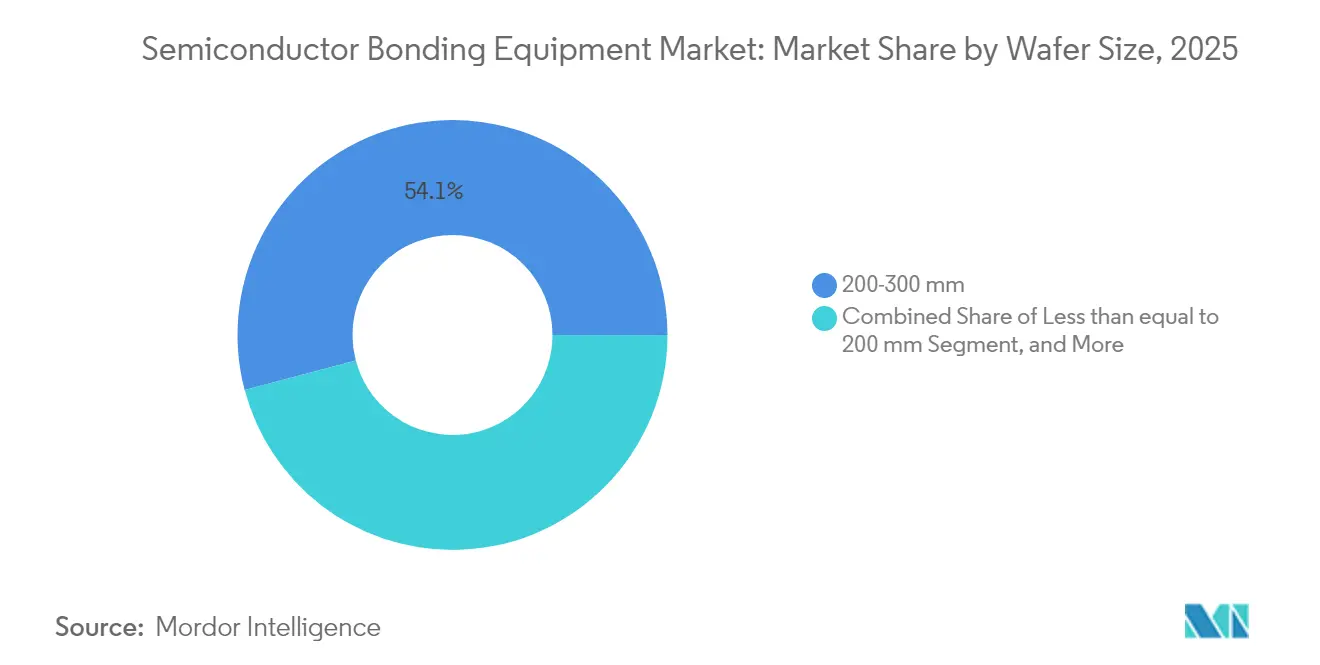
Wafers in the 200-300 mm range delivered 54.12% of 2025 sales, benefiting from well-depreciated fab infrastructure and a robust second-hand tool chain. The category still attracts incremental upgrades such as in-situ metrology modules that retrofit onto existing bonders. In contrast, ≤200 mm formats serve compound semiconductor and mixed-signal nodes where cost per wafer is acceptable at lower volumes. The leap to >300 mm drives the highest momentum, projected at 6.44% CAGR, propelled by mega-fabs that chase die-per-wafer economics for AI and memory macros. Early pilot lines for 330 mm gallium-nitride substrates are already in place at select Asian foundries, hinting at a future realignment of capex priorities.
Tool builders must strike a balance: retain design libraries for legacy clamp sizes and stepper alignment marks while fielding new platforms with extended vacuum chucks and wafer-edge exclusion algorithms. The dual demand profile increases R&D spend yet opens parallel revenue streams. As a result, volume growth in the >300 mm category enlarges the semiconductor bonding equipment market size without cannibalizing mature-node demand.,
By End User: Foundry Momentum Builds
Integrated Device Manufacturers still represented 45.66% of 2025 revenue through captive lines optimized for latency-sensitive parts such as smartphone application processors. However, accelerated outsourcing by fabless houses pushes foundry order books ahead at a 6.32% CAGR. Giants like TSMC, Samsung Foundry, and GlobalFoundries now pitch turnkey heterogenous integration services, consolidating wafer production and packaging in contiguous campuses. Such verticality compels high-mix bonders capable of quick recipe changes. Foundry procurement teams thus prioritize modular platforms that share spares across multiple technology nodes, trimming total service cost.
OSAT players focus on cost-sensitive consumer and IoT segments where standard wire-bond packages remain viable. They continue to buy refurbished units while trialing one or two hybrid systems for premium tiers. The tri-modal customer landscape fosters healthy competition among equipment makers, sustaining order visibility in the semiconductor bonding equipment market across up- and down-cycles.
Geography Analysis
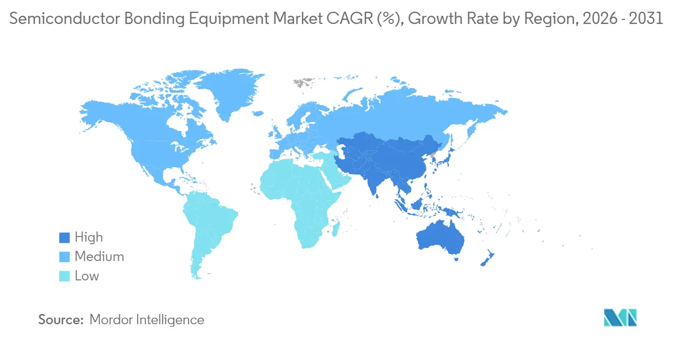
Asia-Pacific held 52.64% of 2025 revenue, underlined by USD 49.6 billion in equipment spending from China alone, up 35% year over year. South Korea followed with USD 20.5 billion, and Taiwan contributed USD 16.6 billion despite temporary inventory corrections. Regional policy packages include tax deductions, duty exemptions, and infrastructure subsidies that lower effective purchase prices of hybrid bonders, sustaining leadership in the semiconductor bonding equipment market. Local champions such as TSMC and Samsung spearhead 3D and hybrid adoption, elevating regional technical standards and reshaping supply-chain expectations for precision chucks and ultra-flat carrier wafers.
North America posted USD 13.7 billion in 2024 sales, advancing 14% alongside CHIPS Act allocations targeting domestic capacity expansion. Intel, Micron, and Texas Instruments have announced multiyear packaging projects anchored in Arizona, Ohio, and Texas. The subsidy stimulus accelerates inbound orders but raises concerns over long-term cost competitiveness once grants taper. Yet the region benefits from proximity to hyperscale-data-center customers demanding low-latency interposers for AI workloads, a segment that outlets more value-added hybrid bonders into the semiconductor bonding equipment market. Europe concentrates spending in Germany and the Netherlands where analog, power, and EUV tool vendors cluster. Collaborative programs like IPCEI-ME/CT channel EUR funding into 3D integration, especially for automotive power modules that require stringent reliability. Middle East and Africa remain nascent, though Saudi Arabia’s Vision 2030 and the UAE’s strategic tech funds have earmarked pilot lines for compound semiconductors. These early moves hint at wider regional diversification that could incrementally enlarge the semiconductor bonding equipment market beyond its traditional APAC stronghold.,

Regulatory Landscape
Regulation affecting semiconductor bonding equipment is increasingly shaped by export-control policy for semiconductor manufacturing equipment and associated upstream inputs. This influences where advanced bonding tools can be shipped, installed, and serviced. In the United States, the Department of Commerce Bureau of Industry and Security (BIS) export controls operate alongside multilateral frameworks such as the Wassenaar Arrangement, with allied alignment involving Japan and the Netherlands. The resulting compliance complexity affects global OEMs and their component suppliers.
A tightening referenced in policy tracking is also expected to affect equipment flows into certain China-based manufacturing footprints. The removal of Samsung and SK hynix PRC facilities from the Validated End-User (VEU) program takes effect December 31, 2025, which adds licensing friction. On the demand side, industrial policy and funding programs shape where bonding capacity is built and qualified. The U.S. CHIPS and Science Act (USD 52.7 billion) and Europe’s semiconductor initiative (EUR 43 billion) have explicit relevance for advanced packaging lines, where wafer-to-wafer and die-to-wafer bonding are core process modules. Industry bodies such as SEMI and the Semiconductor Industry Association (SIA) continue to advocate on trade and export-control implementation details, feeding into vendor planning for localized manufacturing, service coverage, and documentation requirements for advanced bonding platforms.
Value Chain Analysis
The semiconductor bonding equipment value chain begins with upstream precision subsystems (motion control and encoders, optics and machine vision, vacuum pumps and chambers, thermal management hardware, ceramics and chucks) and process materials (adhesives, fluxes, underfills, and carrier wafers). These inputs feed into the tool OEM, which integrates mechanics, process modules, and software controls. Equipment suppliers increasingly co-develop process windows with end users as hybrid and thermo-compression bonding move into higher-volume AI and advanced packaging use cases. Industry collaboration models such as ASMPT and EV Group working on die-to-wafer hybrid bonding for 3D-IC heterogeneous integration illustrate this shift.
Downstream, IDMs, foundries, and OSATs qualify bonders within tightly coupled process flows spanning wafer prep (CMP and cleaning), bonding, and metrology/inspection. Service and spares become a major recurring layer due to utilization and uptime requirements. Export controls and allied trade alignment add a cross-cutting constraint along the chain, extending beyond the finished tool to certain upstream chemical inputs and advanced substrates. That influences lead times and dual-sourcing strategies. As a result, OEMs pair installed-base growth with closer logistics, stronger field-service coverage, and application engineering to shorten qualification cycles at sub-10 um alignment tolerances.
Competitive Landscape
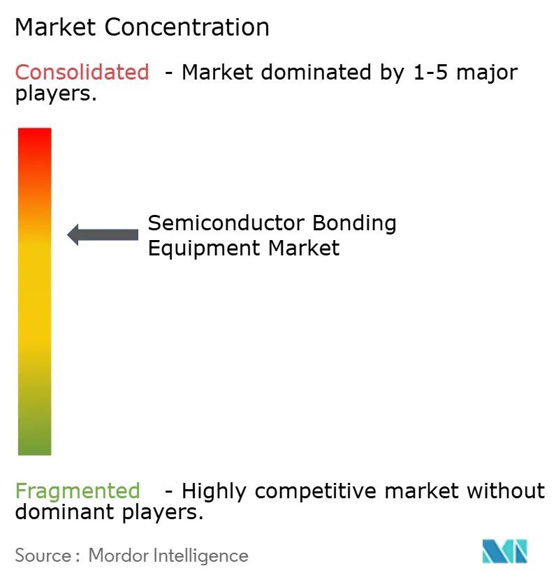
The semiconductor bonding equipment market shows moderate concentration, with five vendors accounting for a significant 2024 revenue. Applied Materials, Tokyo Electron, and ASMPT leverage deep process libraries and service footprints to preserve incumbent status; emerging specialists like EV Group carve niches through sub-micrometer alignment innovations. Strategic alliances proliferate. Applied Materials’ 9% stake in BE Semiconductor Industries strengthens its hybrid-bonding roadmap, allowing co-development of oxide planarization and copper surface-activation modules. Similar tie-ups between tool suppliers and fabs accelerate joint learning cycles, converting bespoke prototypes into volume tools within 18 months instead of the historical 30-month window.
Competition is pivoting from pure throughput metrics to holistic ecosystem integration. Vendors embed machine-learning controllers that predict bond voids, thereby boosting first-pass yield and lowering rework costs. Supply resilience becomes another battleground, with manufacturers dual-sourcing critical components like high-resolution encoders or ceramic heaters to hedge geopolitical disruptions. Price elasticity is limited because performance gains in sub-3 nm nodes outweigh upfront capex. Nonetheless, smaller OSAT customers negotiate performance-based payment schedules to spread risk, compelling vendors to refine lifetime-value calculations in the semiconductor bonding equipment industry.
Looking forward, white-space opportunities lie in silicon photonics and automotive power devices that require field-upgradeable chambers to accommodate new III-V and SiC materials. Patent filings cluster around laser-assisted hybrid bonding and self-learning alignment optics, signaling where the next performance leaps will occur. Meanwhile, stricter sustainability metrics push contenders to develop solvent-free wafer-clean chemistries and low-energy vacuum pumps, differentiators that could tilt RFQs as ESG mandates tighten across the semiconductor bonding equipment market.
Semiconductor Bonding Equipment Industry Leaders
EV Group
ASMPT Semiconductor Solutions
MRSI Systems. (Myronic AB)
WestBond Inc.
Panasonic Holding Corporation
- *Disclaimer: Major Players sorted in no particular order

Market Opportunities and Future Outlook
White space is opening around high-density advanced packaging and heterogeneous integration, where bonding accuracy, contamination control, and in-situ process verification are differentiators beyond throughput alone. Customer qualification activity and vendor roadmaps point to this direction. Samsung initiated a joint evaluation project with ASMPT in April 2026 to qualify thermo-compression bonders for HBM production, reflecting an active effort by a major memory producer to broaden the qualified tool set beyond internal supply. Separately, EV Group and imec demonstrated wafer-to-wafer hybrid bonding at a 200 nm Cu interconnect pitch using the GEMINI FB system (May 2026), which supports equipment platforms designed for tighter interconnect pitches and routable interconnect test vehicles.
Opportunities also extend to bonding-adjacent capability bundles that target lower total cost of ownership and faster ramp time, including integrated surface preparation (such as oxide removal approaches), embedded metrology, and software-driven recipe portability across sites. Vendor-side indicators support this direction. Mycronic reported strong order intake in 1H 2026 with demand in die bonding tied to optical communications and defense applications, and ASMPT cited AI infrastructure pull-through in its SMT-related order momentum. Together, these point to end-market demand that feeds advanced packaging and high-precision assembly requirements. Against export-control scrutiny and regional subsidy programs (for example, CHIPS Act and EU initiatives), tool makers that localize service, documentation, and qualification support have a clearer path to projects that prioritize supply-chain resilience and faster process sign-off.
Recent Industry Developments
- June 2026: ASMPT Semiconductor Solutions secured a repeat order for eight Thermo-Compression Bonding tools for chip-to-wafer applications from a leading global integrated device manufacturer to support client and data center CPU production. The market continues to adopt thermo-compression bonding in AI and HPC packaging. The order reinforces demand for chip-to-wafer bonding and strengthens ASMPT’s presence in AI data-center supply chains.
- May 2026: EV Group and imec demonstrated wafer-to-wafer hybrid bonding technology at 200nm Cu interconnect pitch on a test vehicle using the GEMINI FB bonding system. Hybrid bonding supports next-gen AI accelerators and 3D integration. The demonstration validates industry readiness of hybrid bonding for high-density interconnects and could drive tooling demand for advanced packaging lines.
- February 2026: ASMPT Semiconductor Solutions received an order for two ultrafine pitch Thermo-Compression Bonding tools equipped with plasma Active Oxide Removal technology for chip-to-wafer applications. Ultrafine-pitch TCB adoption is emerging in advanced packaging. The order indicates early uptake of next-gen bonding capabilities and expands ASMPT’s tool footprint in high-end packaging.


Research Methodology Framework and Report Scope
Market Definition and Coverage
For this study, the market covers revenue earned from tools and systems used to bond semiconductor wafers, dies, and packages during back-end assembly and advanced packaging production, including installations and tool-level upgrades counted at equipment selling prices.
Scope exclusions: We exclude bonding consumables, general packaging materials, and stand-alone inspection or test tools that are not sold as bonding equipment.
Segmentation Overview
- By Equipment Type
- Permanent Bonding Equipment
- Temporary Bonding Equipment
- Hybrid Bonding Equipment
- By Application
- Advanced Packaging
- Power IC and Discrete
- Photonic Devices
- MEMS Sensors and Actuators
- Engineered Substrates
- RF Devices
- CMOS Image Sensors
- By Bonding Technology
- Thermocompression Bonding
- Eutectic/Solder Bonding
- Adhesive/Polymer Bonding
- Ultrasonic / Thermosonic Bonding
- Anodic / Fusion Bonding
- By Wafer Size
- Less than equal to 200 mm
- 200-300 mm
- Greater than 300 mm
- By End User
- Integrated Device Manufacturers (IDMs)
- Foundries
- Outsourced Semiconductor Assembly and Test (OSAT)
- Geography
- North America
- United States
- Rest of North America
- South America
- Europe
- Germany
- France
- Rest of Europe
- Asia-Pacific
- China
- Japan
- South Korea
- India
- Rest of Asia-Pacific
- Middle East
- Africa
- North America
Data Sources, Market Sizing, and Validation
Desk Research
Desk research starts with mapping demand drivers for bonding tools using public manufacturing updates and trade signals, and then converting those signals into a realistic equipment spending pool. We used sources such as SEMI publications, the US International Trade Commission trade statistics, the World Semiconductor Trade Statistics program for end-demand direction, and central bank and statistical agency releases for inflation and currency context.
To align supply-side reality with demand trends, we also reviewed company annual reports, investor presentations, and reputable industry press for packaging capacity announcements, utilization commentary, and timing of new tool installations. Where available, we referenced paid subscriptions for company financials and intelligence, patents, and shipment-level trade data to cross-check product positioning and import flows, rather than relying on any single dataset. The sources listed here are illustrative only, and many other public and paid references were used to collect, validate, and clarify data points during the study.
Primary Interviews and Surveys
Primary work focused on validating how bonding tool demand is formed in advanced packaging lines, and which purchase triggers matter most across different customer types. We spoke with a mix of equipment suppliers, process engineers, packaging managers, and procurement stakeholders across major manufacturing regions. These inputs helped us refine assumptions on tool mix, typical upgrade cycles, and price realization. The interviews were also used to confirm how temporary, permanent, and hybrid platforms are selected for different package types and wafer sizes, and to sanity-check the final totals.
Distribution of primary research fieldwork respondents
| Company type | Respondent position | Region |
|---|---|---|
| Top tier: 26% | CXOs: 12% | APAC: 43% |
| Mid tier: 60% | Functional/Unit leaders: 38% | EMEA: 37% |
| Smaller Players: 14% | Managers: 50% | Americas: 20% |
Market-Sizing & Forecasting
The core sizing starts from a top-down build where packaging output and capacity expansion signals are reconstructed into a yearly demand pool for bonding tools by region, and then adjusted for the share of steps that require bonding. From there, selective bottom-up checks are used to keep the totals realistic, including sampled price ranges by tool class, channel feedback on delivery lead times, and a supplier-side roll up for a limited set of widely tracked product lines.
Key inputs used in the model include advanced packaging capacity additions, wafer size mix (200 mm and above), typical tool utilization ranges, replacement and refurbishment timing, and average selling price movement by bonding technology. Where interview feedback pointed to gaps, for example how often hybrid bonding tools are bought as part of a cluster versus stand-alone, assumptions were tightened and then re-tested against the demand pool.
For forecasting, we rely mainly on scenario analysis supported by multivariate regression checks, where the independent variables include packaging capex direction, end-market pull for high bandwidth and high density packages, and regional fab build-out schedules. When data is thin in smaller countries, we fill gaps using proxy indicators like regional capacity shares and import patterns, then validate those splits through follow-up expert checks.
Data Validation & Update Cycle
Outputs are validated through several checks so the final numbers match real-world operating conditions. We compare implied equipment demand against independent signals such as packaging capacity ramps, reported capex cycles, and trade movement patterns, and then review any sharp swings before internal sign-off.
If the model produces unusual price or volume jumps, respondents are re-contacted and assumptions are reworked until the variance can be explained by a documented change, such as a technology shift or timing pull-in. Reports are refreshed annually, and interim updates are made when material events occur that can alter investment timing. Before delivery, an analyst performs a fresh pass so clients receive the latest updated view.
Mordor Intelligence's Semiconductor Bonding Equipment Market Size Versus Other Published Estimates
Published market sizes for bonding equipment often vary because different studies draw the line differently on what counts as bonding equipment revenue, and they also handle timing and currency conversions in their own ways. Differences also show up when some estimates lean heavily on one demand indicator, while others blend several signals and then validate them with direct industry feedback.
The table shows a clear spread that mainly comes from scope and modeling choices around advanced packaging tool mixes, what is treated as bonding versus adjacent assembly steps, and how price progression is carried through the forecast. The table also reflects how some publishers smooth the cycle with longer averaging windows, while others use a more aggressive or conservative capex scenario in years when packaging investments are lumpy.
Benchmark comparison
| Source | Market Size | Gaps in Research Methodology |
|---|---|---|
| Mordor Intelligence | USD 596.47 M (2026) | |
| Global Consultancy A | USD 0.83 B (2026) | Often bundles die attach and certain assembly platform modules into bonding spend, and applies a faster ASP uplift for hybrid bonding tools without consistent checks against utilization and installed base replacement timing. |
| Industry Association B | USD 0.49 B (2026) | Typically focuses on member-reported shipment categories that can undercount refurbishments and upgrade revenue, and it may allocate some advanced packaging tool demand into broader back-end equipment buckets. |
The spread across sources is mostly explained by what gets included alongside bonding tools and how quickly prices and adoption are assumed to move. The table points to over-inclusion on one side and under-capture on the other, and in Mordor Intelligence's model, bonding equipment is counted when the tool is purpose-built for wafer, die, or package bonding, with upgrades and refurbishments included only when they are sold as equipment revenue and confirmed through interview checks.


Key Questions Answered in the Report
What is the current value of the semiconductor bonding equipment market?
The market is valued at USD 596.47 million in 2026.
How fast is the market expected to grow?
It is forecast to log a 4.84% CAGR through 2031.
Which equipment type is expanding the quickest?
Hybrid bonding platforms are rising at a 5.88% CAGR.
Which region leads demand?
Asia-Pacific commands 52.64% of 2025 revenue due to strong foundry spending.
Why are subsidies important?
CHIPS Act and EU programs lower capital risk, accelerating domestic bonding-tool purchases.
What technology trend poses the biggest challenge?
Achieving sub-10 µm alignment tolerances increases process complexity and equipment costs.
Page last updated on: