
Semiconductor And Electronic Parts Manufacturing Market Size and Share
Market Overview
| Study Period | 2020 - 2031 |
|---|---|
| Market Size (2026) | USD 592.62 Billion |
| Market Size (2031) | USD 929.52 Billion |
| Growth Rate (2026 - 2031) | 9.42 % |
| Fastest Growing Market | North America |
| Largest Market | Asia-Pacific |
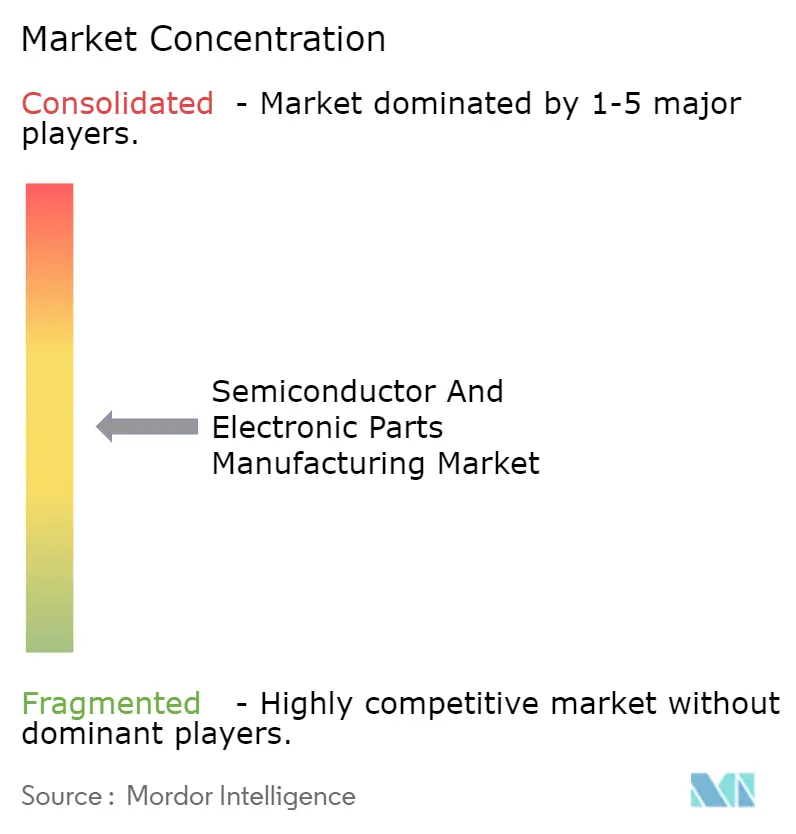
| Market Concentration | Medium |
Major Players *Disclaimer: Major Players sorted in no particular order Image © Mordor Intelligence. Reuse requires attribution under CC BY 4.0. | |
Semiconductor And Electronic Parts Manufacturing Market Analysis by Mordor Intelligence
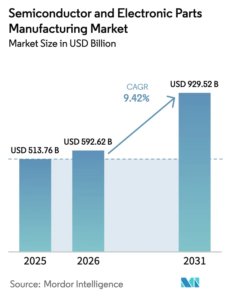
The Semiconductor and Electronic Parts Manufacturing market size is expected to grow from USD 513.76 billion in 2025 to USD 592.62 billion in 2026 and is projected to reach USD 929.52 billion by 2031, expanding at a 9.42% CAGR over 2026-2031. This expansion translates into the swiftest absolute value creation the sector has recorded since the mid-2000s, confirming that structural supply-chain realignment, rather than post-pandemic recovery, is fueling capital formation. Accelerated deployments of artificial intelligence (AI) infrastructure are redefining semiconductor architecture priorities, favoring high-bandwidth memory and advanced packaging over additional node shrinks. Intensified electrification of transport, coupled with the migration to compound-semiconductor power devices, is unlocking premium revenue pools in silicon carbide (SiC) and gallium nitride (GaN). National subsidy programs- most notably the United States CHIPS and Science Act and the European Union Chips Act- have moved over USD 100 billion in direct incentives into fabrication construction pipelines, effectively re-shoring segments of the production footprint that exited these geographies three decades ago.[1] Simultaneously, friend-shoring strategies are broadening mature-node capacity across Vietnam, India and Mexico, while export-control regimes raise compliance hurdles that favor vertically integrated leaders. Risk factors include escalating geopolitical constraints and a shortfall of process engineers specialized in sub-7 nm technologies.
Key Report Takeaways
- By product type, Logic ICs led with 36.54% revenue share in 2025, whereas the Discrete and Power segment is set to record a 10.42% CAGR through 2031.
- By component, Equipment captured 51.26% of the revenue in 2025 and Services are projected to grow at a 10.15% CAGR between 2026 and 2031.
- By application, Communications and Networking captured 30.68% of the revenue in 2025, whereas Data Center and Cloud solutions are forecast to advance at a 10.86% CAGR through 2031.
- By technology node, sub-7 nm accounted for 43.48% of the 2025 revenue and is expected to expand at a 9.88% CAGR through 2031.
- By geography, the Asia-Pacific region accounted for 49.66% of 2025 revenue, while North America is expected to register the fastest regional CAGR of 11.26% through 2031.
Note: Market size and forecast figures in this report are generated using Mordor Intelligence’s proprietary estimation framework, updated with the latest available data and insights as of January 2026.
Market Trends and Insights
Drivers Impact Analysis of Semiconductor And Electronic Parts Manufacturing Market*
| Driver | (~) % Impact on CAGR Forecast | Geographic Relevance | Impact Timeline |
|---|---|---|---|
| AI-led Demand for High-bandwidth Compute | +2.8% | Global, concentrated in North America and East Asia | Medium term (2–4 years) |
| Electrification of Transport Boosting SiC / GaN Content | +1.9% | Global, led by Europe, China and North America | Long term (≥ 4 years) |
| Government Fab-subsidy Race (CHIPS, EU Chips, K-Chips, etc.) | +2.1% | North America, Europe, South Korea, Japan | Short term (≤ 2 years) |
| 5G and Edge-IoT Device Proliferation | +1.2% | Asia-Pacific core, spill-over to Middle East and Africa | Medium term (2–4 years) |
| Chiplet and 3D Heterogeneous Integration Accelerating Node-agnostic Growth | +0.9% | Global, with R&D hubs in North America and Taiwan | Long term (≥ 4 years) |
| Friend-shoring Duplication of Critical Legacy-node Capacity | +0.5% | North America, Europe, Southeast Asia | Medium term (2–4 years) |
| Source: Mordor Intelligence | |||
AI-Led Demand for High-bandwidth Compute
High-bandwidth memory (HBM) shipments expanded 150% year-over-year in 2025, reflecting generative-AI workloads that require 1.2 TB/s bandwidth per package. Hyperscalers have begun co-designing custom accelerators with foundries, compressing merchant GPU addressable markets and positioning advanced package technology as the next competitive frontier. Nvidia’s Blackwell architecture, entering volume shipments in 2026, integrates eight HBM3E stacks, straining clean-room capacity until late-2026 expansions materialize. Data-center retrofits now specify 1.5 MW racks, tripling 2024 power-density baselines and consequently driving demand for SiC modules in grid-tie inverters. Sovereign-AI programs in the United Arab Emirates, Saudi Arabia and India add a further USD 30 billion in localized compute budgets aimed at bypassing export-controlled GPUs. The multiplier extends into network fabrics and thermal-management subsystems, which together add USD 12,000 of semiconductor content per server rack.
Electrification of Transport Boosting SiC / GaN Content
Electric-vehicle semiconductor content reached USD 1,200 per unit in 2025, double the internal-combustion baseline, with SiC inverters contributing 35% of that uplift.[2] Tesla teardown data confirmed SiC module costs below USD 150 per kilowatt, catalyzing uptake in mass-market models priced under USD 30,000. Chinese automakers BYD and Geely are vertically integrating 200 mm SiC wafer lines, challenging Western vendors on cost while yield gaps persist at 25 percentage points. GaN devices, leveraged for on-board chargers, enable 30% volume reductions yet face reliability skepticism under automotive temperature cycling, limiting 2025 platform penetration to 15%. Euro 7 regulations mandating 48 V mild-hybrids across new passenger cars from July 2025 add incremental demand for 300,000 wafer starts per month of power discretes.
Government Fab-Subsidy Race
The United States disbursed USD 29 billion in CHIPS Act grants by December 2025, including USD 6.6 billion for TSMC’s Arizona Fab 21, which targets 3 nm output by 2027. The European Union committed EUR 15 billion (USD 16.4 billion) in direct support through mid-2025, directing EUR 10 billion (USD 10.9 billion) toward Intel’s Magdeburg complex. South Korea’s K-Chips program has pledged KRW 26 trillion (USD 19.5 billion) in tax offsets, accelerating Samsung’s Pyeongtaek P4 facility toward 2 nm volume output in late-2025. These subsidies dilute return-on-capital thresholds and embed overcapacity risks in 28 nm lines, where 1.2 million wafer starts per month are planned across Texas Instruments, GlobalFoundries and United Microelectronics by 2027. “guardrails” compel recipients to freeze expansions in “foreign countries of concern” for 10 years, structurally decoupling U.S. and Chinese ecosystems.
5G and Edge-IoT Device Proliferation
Global 5G subscriptions surpassed 1.9 billion in 2025, yet semiconductor upside pivots to Open RAN and private-network gateways where RF-front-end content stabilizes at USD 18 per handset. Industrial 5G deployments require time-sensitive networking, spurring ASIC integration by Broadcom and Marvell that melds modem and Ethernet functions, capturing 60% of the 2025 edge-switch silicon market. Edge AI inference multiplies compute density at towers tenfold, encouraging operator adoption of custom accelerators from Nvidia and AMD. IoT device consolidation is accelerating as Matter and Thread cut interoperability barriers, placing efficiency leadership with Nordic Semiconductor and Silicon Labs. 3GPP Release 18 mandates RedCap support, opening cost-optimized pathways for industrial sensors priced below USD 5 bill-of-materials.
Restraints Impact Analysis of Semiconductor And Electronic Parts Manufacturing Market*
| Restraint | (~) % Impact on CAGR Forecast | Geographic Relevance | Impact Timeline |
|---|---|---|---|
| Intensifying Geo-economic Export Controls | –1.4% | Global, acute in China–U.S. corridors | Short term (≤ 2 years) |
| IP-Rights Infringement and Cross-licensing Disputes | –0.6% | Global, concentrated in mobile and automotive | Medium term (2–4 years) |
| Acute Talent Shortages in Sub-7 nm Process Engineering | –0.9% | North America, Europe, East Asia | Long term (≥ 4 years) |
| Neon and Advanced-gas Supply-chain Fragility | –0.7% | Global vulnerability in Europe and East Asia | Short term (≤ 2 years) |
| Source: Mordor Intelligence | |||
Intensifying Geo-Economic Export Controls
The U.S. Bureau of Industry and Security’s October 2024 rule expansion added 140 Chinese entities to the Entity List, curtailing access to sub-14 nm tools. ASML’s China revenue declined 35% in 2025 as High-NA EUV shipments pivoted to Europe and North America. China’s counter-measures on gallium and germanium disrupted GaN and SiC supply until Canada and Australia scaled output by mid-2025. Compliance costs now exceed USD 8 million annually for mid-tier suppliers, eroding margins and elongating design cycles to over 90 days. Dual-jurisdiction oversight under ITAR and EAR further slows time-to-market for dual-use innovations.
Acute Talent Shortages in Sub-7 nm Process Engineering
A global deficit of 67,000 process engineers is forecast by 2027, with sub-7 nm expertise concentrated in 12 fabs worldwide.[3] TSMC’s Arizona operations experienced six-month delays stemming from limited local yield-optimization skills, necessitating relocation of 500 Taiwanese engineers. Senior process-engineer compensation in Phoenix reached USD 350,000, a 60% premium over 2022, reducing fab operating margins. Intel’s USD 100 million university partnerships have yet to bridge a 40% graduation gap. Technician training pipelines are equally stressed, with only 3,000 community-college graduates available against 8,000 annual openings. CHIPS Act workforce funds trail construction schedules by 24 months, creating latent start-up risk for new lines.
*Our forecasts treat driver/restraint impacts as directional, not additive. The impact forecasts reflect baseline growth, mix effects, and variable interactions.
Semiconductor And Electronic Parts Manufacturing Market Segment Analysis
By Product Type:
Logic Anchors, Power OutpacesThe Semiconductor and Electronic Parts Manufacturing market size attributed to Logic ICs amounted to 36.54% of 2025 revenue, reflecting sustained demand for application processors and AI accelerators. Memory demand is expected to stabilize after 2026 as new HBM capacity alleviates supply constraints. Analog and mixed-signal components continue to generate significant revenue, driven by their extended life cycles in industrial and automotive applications. Discrete and power devices, are expected to outpace their peers by growing at a 10.42% CAGR, driven by the penetration of SiC and GaN in electric mobility.
Chiplet-based architectures blur these categories by embedding memory and I/O dies from mature nodes alongside cutting-edge compute chiplets, redistributing profit pools toward packaging specialists. Memory’s move to stacked configurations raises the cost of goods but earns pricing power, while analog suppliers defend margins via proprietary high-voltage flows. Chinese entrants are pressuring low-end discrete devices, forcing Western incumbents up-market into 1,200 V SiC, where yields and reliability create entry barriers.


By Component:
Equipment Dominant, Services AscendantEquipment contributed 51.26% of 2025 component revenue, underpinned by multi-billion-dollar lithography outlays. High-NA EUV systems priced at USD 380 million each garnered unprecedented order backlogs. Software remains the strategic gatekeeper to sub-3 nm processes, with Synopsys and Cadence playing a dominant role in the advanced-node toolchain. Services will chart the fastest trajectory at a 10.15% CAGR in the forecast period, mirroring the growing intensity of design outsourcing.
The Semiconductor and Electronic Parts Manufacturing market size for Services is projected to eclipse USD 400 billion by 2031 as fabless firms deepen turnkey partnerships. Equipment vendors increasingly monetize installed bases through spares and predictive-maintenance analytics that carry gross margins exceeding 60%. Software is consolidating vertically, illustrated by Synopsys’ 2024 acquisition of Ansys. Geographic wage differentials steer routine verification tasks to India and Vietnam, while compliance frameworks such as ISO 26262 anchor higher-value audits in mature markets.
By Application:
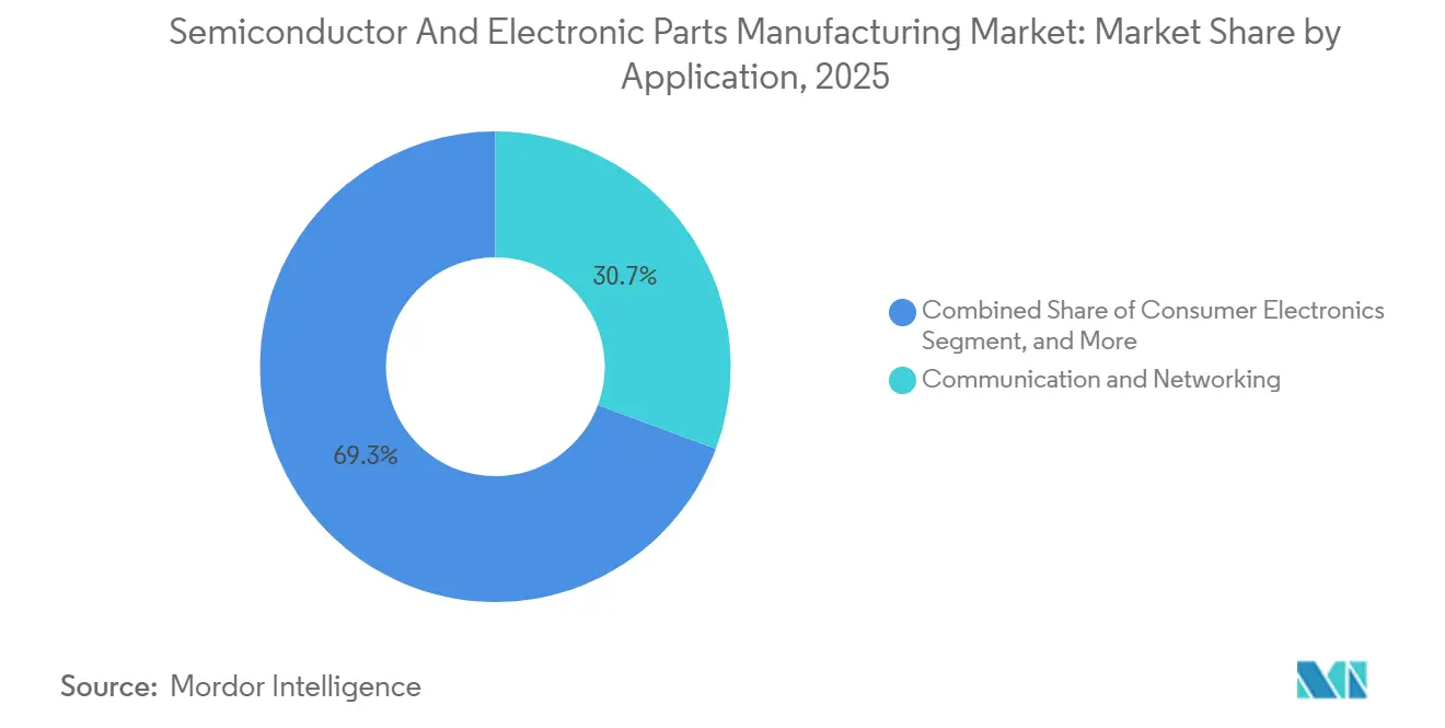
Communications Firm, Data Centers SurgingCommunications and Networking remained the largest application at 30.68% of 2025 revenue, a share it sustains thanks to 5G infrastructure rollouts. Data Center and Cloud is the fastest-growing segment, with a 10.86% CAGR, driven by electric-vehicle inverter and ADAS compute needs. Consumer electronics, while mature, pocket incremental volume in wearables and smart-home devices. Industrial and Energy applications leverage Industry 4.0 automation and grid-modernization programs.
Automotive’s stringent zero-defect metrics necessitate process variants dedicated to functional safety, bifurcating fab utilization. Data-center buyers emphasize throughput per watt, spurring a pivot toward custom ASICs over GPUs for inference. Open RAN disaggregation in communications reallocates silicon value from turnkey base stations to merchant processors.
By Technology Node:
Leading Edge Slows, Mature Nodes ThriveSub-7 nm capacity held 43.48% revenue share in 2025 yet will slow to a 9.88% CAGR as mask-set costs and yield headwinds erode economics. The 8-16 nm tier aligns with automotive and edge AI requirements. The 22-28 nm bracket is experiencing a resurgence driven by chiplet architectures, making it relevant in the Semiconductor and Electronic Parts Manufacturing market over the forecast period. Nodes beyond 28 nm, previously considered outdated, continue to see demand due to their applications in the analog and power markets.
TSMC’s 3 nm node yielded only 15% performance uplift at 2.5 times wafer cost, shrinking its accessible market, while Samsung’s 2 nm gate-all-around process promises gains but remains yield-limited. Intel’s 18A roadmap embeds backside power delivery to regain leadership by 2027. Chinese foundries expand mature nodes even under export restrictions, depressing 28 nm wafer pricing.
Geography Analysis
APAC Semiconductor and Electronic Parts Manufacturing Market
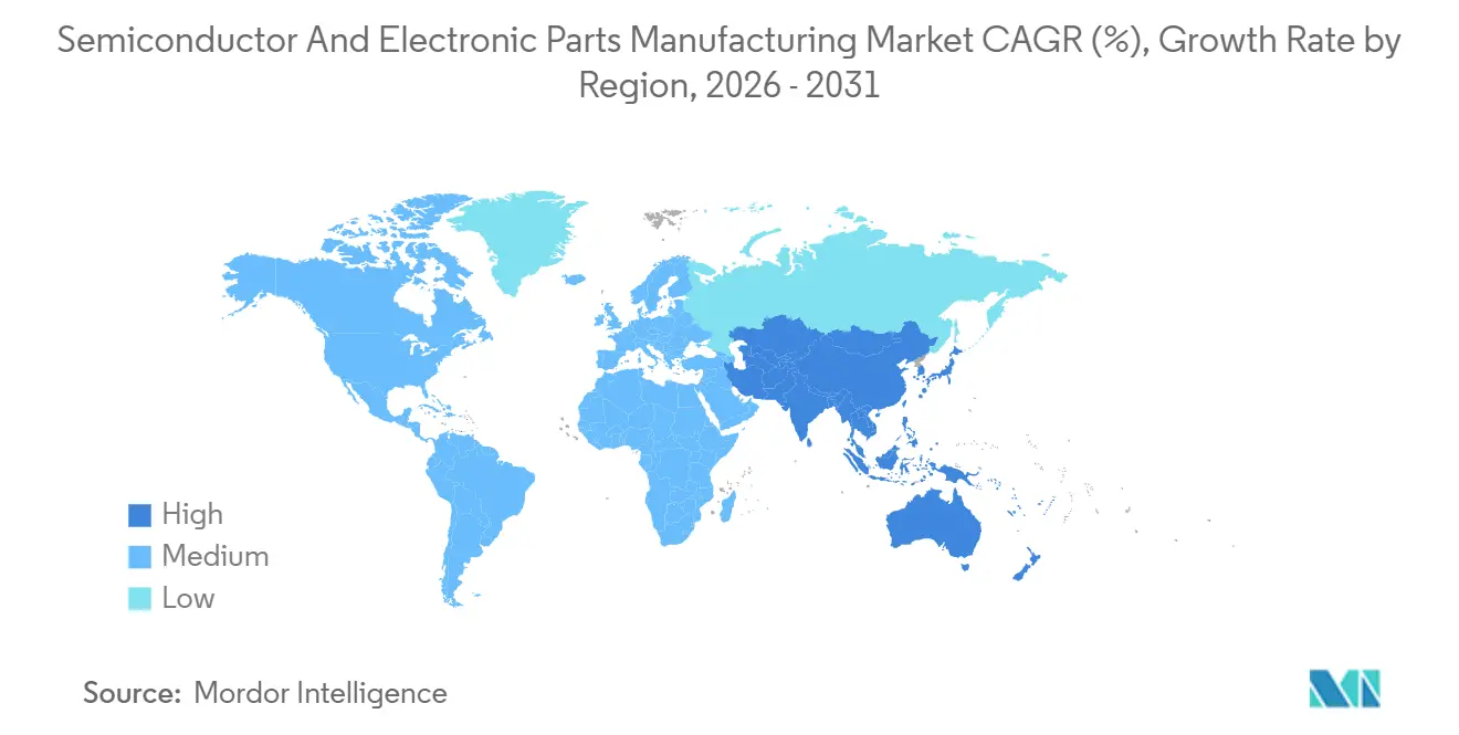
Asia-Pacific accounted for 49.66% of global revenue in 2025, with Taiwan and South Korea leading-edge logic and memory. The region’s growth is expected to be moderate as geopolitical diversification spreads capacity across India, Vietnam, and Malaysia. China remains the largest single-country buyer, yet export controls limit its access to advanced tools. Japan, boosted by double-digit subsidies, is resurgent in 22–28 nm lines through TSMC’s Kumamoto joint venture. India regains relevance in the back end as Micron and AMD build test and assembly campuses.
North America Semiconductor and Electronic Parts Manufacturing Market
North America is set to record the swiftest CAGR of 11.26% through 2031, as CHIPS Act subsidies underwrite 12 new front-end fabs. The United States’ Semiconductor and Electronic Parts Manufacturing market size is estimated to grow rapidly by 2031, reversing a three-decade offshoring trend. Canada advances as a SiC materials hub, while Mexico scales OSAT capacity for near-shore automotive supply chains.
EMEA Semiconductor and Electronic Parts Manufacturing Market
Europe is aiming to increase its global presence by 2030 through a EUR 43 billion subsidy pool. Germany hosts the flagship Intel Magdeburg plant, while France specializes in SiC through STMicroelectronics. The Middle East channels sovereign wealth toward AI-focused fabs, though domestic ecosystems remain at pilot scale. Africa’s footprint is nascent but growing via consumer-electronics assembly in South Africa and Nigeria.
Regulatory Landscape
The regulatory environment is increasingly shaped by trade actions, export controls, and subsidy-linked compliance requirements that affect where advanced-node capacity and critical equipment can be sourced and deployed. In the United States, a January 2026 presidential proclamation introduced a 25% ad valorem tariff on certain imported semiconductors, semiconductor manufacturing equipment, and derivative products, which adds cost and documentation burdens for cross-border supply chains.
Export-control and procurement rules also tighten constraints for suppliers serving sensitive end markets. The U.S. Bureau of Industry and Security updated license review policy for certain advanced computing semiconductors exported to China under strict conditions, while the Federal Acquisition Regulatory Council issued a February 2026 proposed rule to implement Section 5949 of the FY23 NDAA. That rule would prohibit executive agencies from procuring covered semiconductor products or services from specified Chinese entities, including SMIC, CXMT, and YMTC, with the prohibition tied to a December 23, 2027 effective date.
Value Chain Analysis
The value chain runs from upstream materials and specialty gases, to wafer manufacturing and equipment, to front-end fabrication by IDMs and foundries, and then to back-end assembly, test, and advanced packaging, before products reach OEM and hyperscaler-led end markets. Policy-driven localization is already influencing footprint decisions across these steps, including July 2026 announcements covering TSMC's plan for an additional USD 100 billion investment for Arizona expansion (bringing its total planned US investment to USD 265 billion) and Intel's EUR 5 billion commitment to expand manufacturing at Leixlip, Ireland. Together, these moves further concentrate activity around regional equipment and materials ecosystems.
Memory and packaging constraints are also reshaping relationships among designers, memory suppliers, and substrate and OSAT partners. In June 2026, NVIDIA and SK hynix announced a multiyear technology partnership to co-develop next-generation memory for AI infrastructure, reinforcing a shift from transactional purchasing to co-engineering. On the materials side, GlobalWafers and Micron moved toward a 10-year long-term agreement in July 2026, supported by Micron strategic financing for US operations, which underscores the value of long-duration supply assurance as lead times remain long for complex lithography and process-control tools. Talent shortages in packaging and test add additional friction for near-term ramping.
Competitive Landscape
The leading edge is oligopolistic: TSMC, Samsung and Intel own 85% of sub-7 nm capacity. Conversely, the legacy tier remains fragmented across more than 15 players, giving automotive and industrial customers leverage to dual-source. Foundries are monetizing process IP licensing as fabless designers forego proprietary node development. Capital intensity shifts margin pressure to equipment vendors that must commit to multi-generational backward compatibility.
Chiplet ecosystems unlock greenfield niches for startups capable of delivering specialized dies that integrate via UCIe interfaces without building fabs. Chinese producers SMIC and Hua Hong push mature-node performance envelopes through advanced packaging, approximating 7 nm results at 14 nm geometry. Analog leaders Texas Instruments and Analog Devices defend 65% combined gross margins via differentiated high-voltage flows. RISC-V adoption eclipses 10 billion shipped cores, challenging Arm’s incumbent royalty model. Patent trends show TSMC filing 1,200 gate-all-around and backside-power patents in 2025, cementing IP leadership through the decade.
Semiconductor And Electronic Parts Manufacturing Industry Leaders
-
Intel Corporation
-
Samsung Electronics Co. Ltd
-
Taiwan Semiconductor Manufacturing Co. Ltd.
-
SK Hynix Inc.
-
Micron Technology Inc.
- *Disclaimer: Major Players sorted in no particular order
Semiconductor And Electronic Parts Manufacturing Market Companies Covered in this Report
- Taiwan Semiconductor Manufacturing Co. Ltd.
- Samsung Electronics Co. Ltd.
- Intel Corp.
- SK Hynix Inc.
- Micron Technology Inc.
- Qualcomm Technologies Inc.
- Broadcom Inc.
- Texas Instruments Inc.
- Analog Devices Inc.
- NXP Semiconductors N.V.
- STMicroelectronics N.V.
- Infineon Technologies AG
- ON Semiconductor Corp.
- Renesas Electronics Corp.
- Nvidia Corp.
- Advanced Micro Devices Inc.
- GlobalFoundries Inc.
- United Microelectronics Corp.
- Semiconductor Manufacturing International Corp.
- ASE Technology Holding Co. Ltd.
- Lam Research Corp.
- Applied Materials Inc.
- KLA Corp.
Read Analysis of Semiconductor And Electronic Parts Manufacturing Companies
Market Opportunities and Future Outlook
Government programs and subsidy pipelines continue to open whitespace across regions and across the stack beyond leading-edge logic, especially in advanced packaging, compound semiconductors, and pilot-line commercialization. In July 2026, India expanded policy support when the Union Cabinet approved Semicon 2.0 with a budget of INR 1,27,500 crore, explicitly targeting machine and material manufacturing, advanced packaging, and compound semiconductors. In Europe, the European Commission proposed Chips Act 2.0 in June 2026, emphasizing pilot lines and emerging domains such as photonic integrated circuits and quantum chips, with opportunities tied to technologies where heterogeneous integration reduces reliance on continuous node shrinks.
In North America, a funded project pipeline is supporting capacity and ecosystem buildout across memory, power devices, and packaging. In July 2026, the US Department of Commerce announced a direct funding agreement of USD 225 million for Robert Bosch Semiconductor LLC tied to a USD 2 billion silicon carbide investment in Roseville, California, reinforcing commercialization pathways for SiC devices linked to electrification. The same month, Micron marked progress at its Clay, New York fab site with a first-concrete milestone, and NIST cited TSMC plans that raise total planned US investment to USD 265 billion, pointing to broad-based demand pull for domestic supply, including advanced packaging capacity increasingly central for AI accelerators and HBM integration.
Recent Industry Developments in Semiconductor And Electronic Parts Manufacturing Market
- July 2026: TSMC announced an additional USD 100 billion investment in the United States, bringing total planned US investment to USD 265 billion for a 12-facility footprint in Arizona spanning advanced manufacturing and packaging. This reinforces geographic diversification of leading-edge capacity and deepens the local ecosystem needed for advanced packaging and high-value process integration.
- December 2025: TSMC announced a USD 12 billion expansion of Arizona Fab 21 to add 2 nm production by 2028, including a CoWoS packaging plant. Adding packaging alongside front-end capacity addresses AI-driven demand for heterogeneous integration and reduces dependence on offshore advanced packaging for high-bandwidth compute platforms.
- October 2024: The US Bureau of Industry and Security expanded export controls by adding 140 Chinese entities to the Entity List, tightening access to sub-14 nm tools. The action increased compliance and licensing burdens across equipment and component suppliers and accelerated supply-chain redesign toward jurisdictions and customers with clearer export-control pathways.
Semiconductor And Electronic Parts Manufacturing Market Report Scope and Research Methodology
Market Definition and Coverage
This market covers revenue generated from manufacturing semiconductor devices and closely related electronic parts, counted at the point of production and shipment, and reported in USD for a global view.
Scope exclusions: We exclude downstream electronics assembly and device brands, and we also avoid double counting of resale and distribution markups outside manufacturing.
Segments Covered in This Report
- By Product Type
- Logic IC
- Memory (DRAM, NAND, Emerging)
- Analog and Mixed-Signal
- Discrete and Power (SI, SiC and GaN)
- Data- Center and Cloud
- By Component
- Equipment (Front-end, Back-end)
- Software (EDA, IP Cores)
- Services (Design, Assembly, Test)
- By Application
- Communications and Networking
- Transportation and Mobility
- Consumer Electronics
- Industrial and Energy
- Data- Center and Cloud
- By Technology Node
- Less than 7nm
- 8- 16 nm
- 22- 28 nm
- Greater than 28 nm
- By Geography
- North America
- United States
- Canada
- Mexico
- South America
- Brazil
- Argentina
- Rest of South America
- Europe
- Germany
- United Kingdom
- France
- Italy
- Spain
- Rest of Europe
- Asia-Pacific
- China
- Japan
- India
- South Korea
- ASEAN
- Rest of Asia-Pacific
- Middle East
- Saudi Arabia
- United Arab Emirates
- Rest of Middle East
- Africa
- South Africa
- Nigeria
- Rest of Africa
- North America
Data Sources, Market Sizing, and Validation
Desk Research
Desk research helped us map the supply chain and build the initial demand signals that manufacturing output tends to follow. We relied on public and official sources such as World Semiconductor Trade Statistics releases, Semiconductor Industry Association updates, industrial production and trade statistics from agencies such as the US Census Bureau and Eurostat, and macro series from sources such as the World Bank and OECD.
To keep assumptions realistic, we also reviewed annual reports, investor decks, and earnings commentary from listed manufacturers, followed by reputed press coverage on capacity additions and policy programs. Where needed, we used a paid company financials and intelligence subscription, an import and export shipment level database, and a patent database to cross check directionality for technology transitions. These sources are not exhaustive, and many other references were used to collect data, confirm definitions, and clarify specific datapoints.
Primary Interviews and Surveys
Primary interviews and surveys were used to test the model logic against how the market actually behaves across regions and end uses. We spoke with a mix of manufacturers, equipment and materials stakeholders, and buyers in data center, communications, automotive, and industrial supply chains, which then helped close gaps on utilization, pricing movement, and shipment timing across APAC, EMEA, and the Americas.
Distribution of primary research fieldwork respondents
| Company type | Respondent position | Region |
|---|---|---|
| Top tier: 38% | CXOs: 13% | APAC: 41% |
| Mid tier: 40% | Functional/Unit leaders: 27% | EMEA: 33% |
| Smaller Players: 22% | Managers: 60% | Americas: 26% |
Market-Sizing & Forecasting
The core sizing uses a top-down approach where manufacturing revenue is reconstructed from product category sales, regional demand patterns, and technology mix shifts, and then aligned to a single global total without double counting. The output is then checked with selective bottom-up approximations, such as sampled ASP multiplied by shipment volumes for key device families, plus supplier roll ups for a limited set of publicly visible manufacturers to see whether totals feel reasonable.
A few inputs that materially influence the model include worldwide semiconductor sales series, the split between logic and memory cycles, node migration pace (less than 7nm versus mature nodes), data center and AI server buildouts, automotive electrification content growth (including power devices), and capacity expansion timing that affects utilization. When some inputs are not available at a fine level by country or node, the missing pieces are handled through ratio based allocation anchored on publicly reported regional splits and then verified through interviews.
For forecasting, we leaned on scenario analysis supported by short cycle indicators, because pricing and utilization can swing quickly in this industry. The scenarios were tuned using interview feedback on expected wafer starts, inventory normalization, and the pace of advanced packaging and node transitions, and then converted into annual revenue paths with consistent currency and timing assumptions.
Data Validation & Update Cycle
We validate results through multiple checks, where totals are compared against independent signals such as published global sales series, regional growth rates, and implied pricing changes by major device categories. Variances are investigated by tracing back to the driver, which is often an assumption on utilization, a timing shift in capacity, or an overly aggressive ASP curve, and then adjusted before sign off.
A second analyst review is completed to confirm that definitions, math, and year alignment are consistent across the model. Reports are refreshed annually, and interim updates are made when major events materially change supply or demand (such as large capacity announcements or sudden end market shocks). Before delivery, we run a final pass so clients receive the latest updated view based on the most recent data available.
Mordor Intelligence's Semiconductor and Electronic Parts Manufacturing Market Size Compared Against Other Published Estimates
Published market values for this space often differ because each publisher draws the line between device sales, manufacturing services, and broader electronics components in its own way, and the currency timing is not always the same. Differences also show up when a study uses a single year snapshot versus a forward looking base year that reflects a newer cycle point.
Another driver is how the model treats adjacent items such as equipment, software, and services tied to semiconductor production, plus whether technology node mix and end use demand are explicitly built into the math. A spread is also created when one estimate leans heavily on a single global sales series, while another builds a fuller manufacturing view across product types, applications, nodes, and regions with annual refresh triggers, which is the approach applied by Mordor Intelligence.
Benchmark comparison
| Source | Market Size | Gaps in Research Methodology |
|---|---|---|
| Mordor Intelligence | USD 513.76 B (2025) | |
| Industry Association A | USD 791.70 B (2025) | This figure reflects global semiconductor sales, which can sit above a manufacturing only view when broader device sales coverage and reporting conventions are used, and it does not spell out treatment of equipment and related services. |
| Trade Statistics Body B | USD 795.60 B (2025) | This estimate is presented as worldwide semiconductor sales and is typically built from shipment statistics, which can differ from a manufacturing market model that separates components, applications, and node mix to avoid scope overlap. |
The table shows that the main swing comes from scope and what is being counted as the market, not from small math differences. By keeping the definition tied to manufacturing revenue and then stress testing it using sales series, cycle indicators, and interview led checks on utilization and pricing, the result stays traceable to clear inputs and repeatable steps.
Key Questions Answered in the Report
How large will global semiconductor and electronics parts sales be by 2031?
Revenue is forecast to reach USD 929.52 billion by 2031, expanding at a 9.42% CAGR from the 2026 baseline.
Which regional market is set to grow the fastest over the next five years?
North America posts the quickest trajectory at an 11.26% CAGR, fueled by CHIPS Act–backed fab construction.
What component category shows the highest growth potential?
Services, encompassing outsourced physical design and verification, are projected to rise at a 10.15% CAGR.
How do export-control rules affect Chinese semiconductor manufacturers?
Expanded Entity List restrictions deny advanced lithography tools, causing a 35% revenue hit for top equipment vendors in China and compelling local firms to innovate at mature nodes.
What is driving the surge in high-bandwidth memory demand?
Generative-AI training clusters and data-center GPUs require multi-terabyte per second bandwidth, pushing HBM shipments up 150% year-over-year in 2025.