
Probe Card Market Size and Share
Market Overview
| Study Period | 2020 - 2031 |
|---|---|
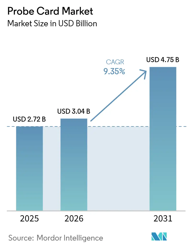
| Market Size (2026) | USD 3.04 Billion |
| Market Size (2031) | USD 4.75 Billion |
| Growth Rate (2026 - 2031) | 9.35% CAGR |
| Fastest Growing Market | Middle East |
| Largest Market | Asia Pacific |
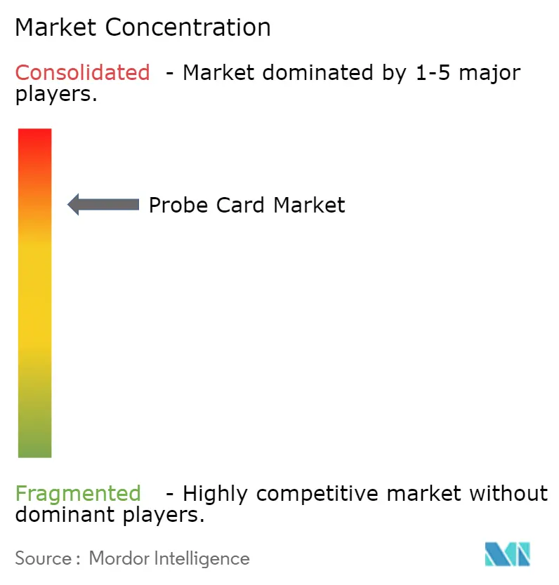
| Market Concentration | High |
Major Players
*Disclaimer: Major Players sorted in no particular order Image © Mordor Intelligence. Reuse requires attribution under CC BY 4.0. |
|
Probe Card Market Analysis by Mordor Intelligence
The Probe Card Market size is expected to increase from USD 2.72 billion in 2025 to USD 3.04 billion in 2026 and reach USD 4.75 billion by 2031, growing at a CAGR of 9.35% over 2026-2031.
This growth mirrors the structural pivot toward sovereign semiconductor capacity, a push reinforced by the United States CHIPS and Science Act’s USD 52.7 billion outlay, Europe’s EUR 43 billion (USD 47 billion) Chips Act, and parallel incentives in Japan and the Middle East. Increasing adoption of heterogeneous integration, especially chiplets and 3D stacks, is moving more test activity to the wafer stage, raising average probe card content per device. Vertical MEMS designs are supplanting cantilever formats as leading-edge nodes impose sub-60-micrometer pitches, while AI accelerators drive demand for advanced cards capable of sustaining frequencies beyond 56 gigahertz. In parallel, public subsidies have shortened fab build schedules to 24 months, front-loading test equipment orders and elevating near-term unit volumes. Foundry and logic producers still represent the single-largest customer block, but OSATs are the fastest-growing buyers as chiplet assembly migrates outside captive fabs.
Key Report Takeaways
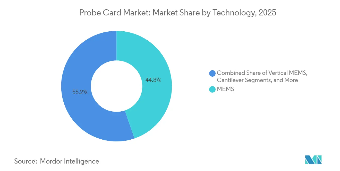
- By technology, MEMS architectures held 44.76% of probe card market share in 2025 and vertical MEMS variants are on track for a 10.63% CAGR through 2031.
- By application, flash memory is projected to expand at an 11.02% CAGR through 2031, the quickest across all segments, compared with foundry and logic’s 9.3% expansion.
- By type, standard designs captured 52.17% of the probe card market share in 2025, yet advanced cards are rising at 11.41% CAGR on AI test complexity.
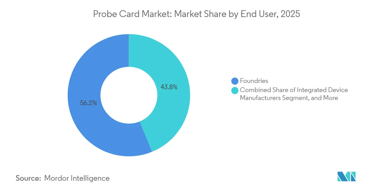
- By end user, outsourced semiconductor assembly and test providers registered the highest growth at 12.27% CAGR, while foundries retained 56.21% spending share in 2025.
- By wafer size, the 300 mm category represented 61.47% of volume in 2025 and will progress at a 9.56% CAGR to 2031.
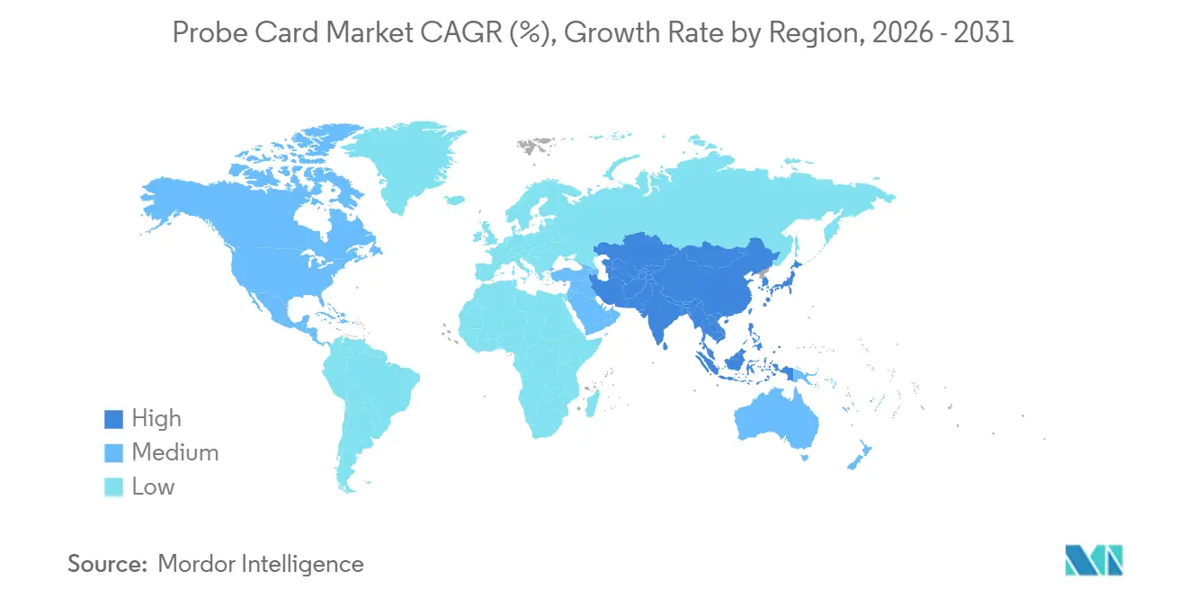
- By geography, Asia Pacific commanded 84.12% of 2025 revenue, whereas the Middle East is the fastest-growing region at 10.06% CAGR.
Note: Market size and forecast figures in this report are generated using Mordor Intelligence’s proprietary estimation framework, updated with the latest available data and insights as of January 2026.
Global Probe Card Market Trends and Insights
Drivers Impact Analysis*
| Driver | (~) % Impact on CAGR Forecast | Geographic Relevance | Impact Timeline |
|---|---|---|---|
| Rising Demand for Consumer Electronics and IoT Devices | +1.8% | Global, with concentration in Asia Pacific manufacturing hubs | Medium term (2-4 years) |
| Miniaturization of Semiconductor Devices | +2.1% | Global, led by Taiwan, South Korea, and United States advanced nodes | Long term (≥ 4 years) |
| Growth in Advanced Packaging and 3D IC Technologies | +2.3% | Asia Pacific core, spillover to North America and Europe | Long term (≥ 4 years) |
| Momentum in Foundry Expansion Incentive Programs | +1.9% | North America, Europe, Middle East, with secondary effects in Asia Pacific | Short term (≤ 2 years) |
| Shift Toward <60 µm Vertical MEMS Probe Cards | +1.4% | Taiwan, South Korea, Japan, United States leading-edge fabs | Medium term (2-4 years) |
| Adoption of AI-Assisted Probe Card Alignment Systems | +1.2% | Global, early adoption in high-volume foundries | Medium term (2-4 years) |
| Source: Mordor Intelligence | |||
Rising Demand for Consumer Electronics and IoT Devices
Smartphone shipments stabilized at 1.2 billion units in 2025, but semiconductor content per handset climbed 18%, led by dedicated AI engines and advanced power-management ICs. Automotive electronics spending reached USD 82 billion in 2025, as electric vehicles now integrate up to 3,000 chips per unit. The installed IoT base surpassed 16 billion devices, with industrial and healthcare endpoints demanding mixed-signal validation across temperature extremes. These shifts decouple probe card demand from mere unit counts, keeping wafer-level test floors busy even when consumer volume plateaus. Apple’s custom M4 processors, introduced in 2025, further spotlight vertical integration strategies that require bespoke probe solutions for unified memory architectures.
Miniaturization of Semiconductor Devices
TSMC moved to volume production of its 2 nm gate-all-around process in late 2025, necessitating probe tips that position within 10 micrometers while avoiding pad damage.[1]TSMC, “Technology Symposium 2025 Proceedings,” tsmc.com Intel’s forthcoming 18A node introduces backside power delivery, compelling dual-sided probing that traditional cantilever cards cannot address. Samsung’s roadmap toward 1.4 nm has doubled probe replacement frequency versus 5 nm processes, lifting per-wafer test costs and tightening supplier qualification windows. Extreme ultraviolet exposure has also introduced localized yield detractors detectable only through wafer-level parametric testing, intensifying the reliance on high-precision probe cards.
Growth in Advanced Packaging and 3D IC Technologies
Heterogeneous integration is shifting test upstream: AMD’s MI300 accelerators combine 13 chiplets that each require 112 gigabit-per-second interface validation prior to dicing. High-bandwidth memory stacks now exceed 200 million units annually, with each wafer requiring through-silicon via continuity checks across 12–16 vertical dies. OSATs are pouring capital into hybrid bonding tools with 2 micrometer alignment, an investment that demands more rigorous known-good-die screening. Universal Chiplet Interconnect Express is standardizing die-to-die signaling, yet probe card interfaces for pre-bond test lack uniformity, prompting a surge in bespoke designs.
The United States dispatched USD 8.5 billion in CHIPS grants to Intel in early 2025, compressing probe card qualification timelines to under a year for Arizona’s new lines. GlobalFoundries, armed with USD 1.5 billion, is adding 50% capacity in New York, translating into roughly USD 45 million of incremental card purchases by 2027. Japan allocated JPY 2 trillion (USD 13.4 billion) for domestic fabs, driving local sourcing mandates that increase sales for Micronics Japan and Japan Electronic Materials. Europe’s EUR 3.3 billion (USD 3.6 billion) package for a 300 mm line in France likewise accelerates demand as 2026 tool move-ins require early test-cell provisioning.[2]European Commission, “European Chips Act Fact Sheet,” ec.europa.eu
Restraints Impact Analysis*
| Restraint | (~) % Impact on CAGR Forecast | Geographic Relevance | Impact Timeline |
|---|---|---|---|
| High Cost of Advanced Probe Card Development | -1.6% | Global, most acute in regions with limited foundry scale | Long term (≥ 4 years) |
| Complexity of Testing at Sub-5 nm Nodes | -1.3% | Taiwan, South Korea, United States advanced foundries | Medium term (2-4 years) |
| Cyclical Nature of Semiconductor Capital Expenditure | -0.9% | Global, with amplified volatility in memory-dependent regions | Short term (≤ 2 years) |
| Limited Availability of Ultra-Low-Resistance Probe Materials | -0.7% | Global supply chain, impacting all advanced node production | Medium term (2-4 years) |
| Source: Mordor Intelligence | |||
High Cost of Advanced Probe Card Development
A leading-edge probe card can cost more than USD 2.5 million, covering iterative prototyping, material science, and multi-temperature validation, costs that only the largest fabs can amortize.[3]FormFactor Inc., “2025 Form 10-K,” investor.formfactor.com Fragmentation in chiplet architectures further erodes volumes per design, blunting scale economies. Smaller fabs face prohibitive switching expenses, locking them into incumbent suppliers and stretching qualification cycles to a year. Suppliers absorb heavy capex for cleanrooms and sub-micron machining, constraining new entrants despite rising end-market volumes.
Complexity of Testing at Sub-5 nm Nodes
Probe pads below 30 micrometers require positioning tolerances within 3 micrometers; deviations risk shorts or dielectric fracture. Contact current density now exceeds 15 mA / µm², halving probe tip lifetimes relative to 7 nm nodes. Designs with 20+ power domains need integrated delivery networks sourcing 200 amperes while holding millivolt regulation, capabilities confined to vertical MEMS topologies. High-speed SerDes above 56 Gbps forces impedance control within 2 ohms along each path, a tolerance that drifts as tips wear. Qualification windows have stretched to 12 months, delaying revenue ramps and elevating the risk that a card becomes obsolete before it ships.[4]Applied Materials, “Investor Day 2025 Presentation,” appliedmaterials.com
*Our forecasts treat driver/restraint impacts as directional, not additive. The impact forecasts reflect baseline growth, mix effects, and variable interactions.
Segment Analysis
By Technology: MEMS Architectures Bridge Sub-5 nm Test Gaps
MEMS designs captured 44.76% of 2025 revenue, owing to contact densities above 10,000 pads and positional accuracy better than 5 micrometers, metrics critical for gate-all-around processes. Vertical MEMS is the fastest mover, clocking a 10.63% CAGR as foundries migrate below 3 nm and adopt backside power rails. FormFactor’s sub-60 micrometer pitch platform, launched in 2025, lets fabs probe chiplet interconnects exceeding 100 pads per mm². Cantilever cards linger in mature nodes due to lower cost, yet their share continues to slip as test teams consolidate tooling portfolios.
First-pass yield hinges on spring-constant uniformity: vertical MEMS maintains ±5% variation versus ±20% for cantilevers, elevating contact reliability in wafer-level burn-in. Japanese suppliers expanded capacity by 40% in 2025 to serve local fabs demanding ultra-fine-pitch solutions. AI-assisted alignment shortens setup cycles by 30%, enabling MEMS cards to achieve 99.5% contact on first touchdown, a throughput imperative for today’s high-volume lines. Specialty formats such as membrane cards retain relevance in RF validation and power-device probing tied to automotive electrification.


By Application: Flash Memory Testing Accelerates on 3D NAND Scaling
Foundry and logic dominated with 47.59% share in 2025, but flash memory is expanding at 11.02% CAGR as 3D NAND layers breach the 200-stack threshold, inflating test vectors per wafer. Samsung’s 286-layer V-NAND required cards able to probe 16 dies simultaneously to hit throughput targets. DRAM unit volumes plateau around DDR5, yet high-bandwidth variants in AI servers sustain incremental demand through stacked dies.
Parametric monitoring now covers 15 points per wafer on Intel’s 18A flow, lifting card consumption per lot by 25% over 7 nm baselines. Analog, mixed-signal, and power devices gain tailwinds from automotive safety norms mandating 100% wafer screening. Chiplet convergence is blurring application lines, spurring hybrid cards that combine logic speed tests with high-speed memory eye scans in one touchdown.
By Type: Advanced Designs Ride AI Accelerator Wave
Standard cards still hold 52.17% share serving nodes above 10 nm, yet advanced formats are trending at an 11.41% CAGR thanks to AI accelerators demanding 112 Gbps integrity, 500 A power delivery, and 300 W thermal loads. Nvidia’s H200 GPU, at 141 billion transistors across eight chiplets, compelled a probe architecture merging coaxial tips with impedance-matched lines up to 67 GHz.
Foundry roadmaps below 5 nm have tilted procurement mixes toward advanced cards: TSMC’s 2 nm ramp allocated 70% of new orders to the category. A middle tier is forming where legacy cards inherit niche upgrades, high-current rails or RF stubs, balancing cost with capability. SEMI E142 interface standards foster mechanical interoperability, yet the absence of electrical spec harmonization perpetuates supplier fragmentation.
By End User: OSATs Scale Through Chiplet Assembly
Foundries retained 56.21% spending in 2025, but OSAT purchases are climbing at 12.27% CAGR as packaging houses invest in chiplet assembly. ASE Technology earmarked USD 1.2 billion for probe infrastructure adaptable to known-good-die validation, signaling a pivot from traditional back-end services. Integrated device manufacturers selectively outsource mature-node testing, fueling volumes of standard cards at OSAT lines.
Research bodies command a modest 2% of demand yet influence roadmaps through trailblazing work, such as IMEC’s sub-1 nm transistors that expose material incompatibilities with existing probe metals. Fast-growing OSAT volumes have triggered regional service centers: Amkor’s 2025 tie-up with a Korean supplier exemplifies collaborative engineering targeting hybrid designs. Foundries counter by bundling fabrication and test, leveraging proprietary process knowledge to optimize card parameters for yield uplift.
By Wafer Size: 300 mm Retains Primacy Amid 450 mm Uncertainty
The 300 mm format captured 61.47% of 2025 shipments and will post a 9.56% CAGR through 2031. TSMC budgeted 85% of its USD 30 billion 2025 capex to 300 mm builds, extending the format’s relevance for the decade. 200 mm lines persist in analog and power markets but grow at just a 4% CAGR, limited by capital re-allocation to advanced nodes.
Industry enthusiasm for 450 mm cooled as Intel shelved its pilot, redirecting funds to advanced packaging. Over 200 global 300 mm fabs equate to USD 10–20 billion sunk per site, encouraging operators to squeeze residual productivity rather than tackle USD 15 billion 450 mm tool sets. Probe suppliers now focus on throughput gains, parallel die testing and automated tip cleaning that adds 40% life, rather than a new wafer diameter. Chiplets alleviate die-size constraints, reducing economic impetus for larger wafers.
Geography Analysis
Asia Pacific retained 84.12% of 2025 revenue, anchored by Taiwan’s 45% share of global demand, South Korea’s memory leadership, and Japan’s domestic content policies. Taiwan’s probe card ecosystem benefits from TSMC’s 2 nm ramp and the company’s USD 40 billion U.S. build, which still sources cards from home suppliers for process continuity. South Korea’s Samsung and SK Hynix shipped more than 250 million high-bandwidth stacks in 2025, needing specialty cards for through-silicon via tests. Japan’s cluster gained momentum as local content rules at the Kumamoto fab steered purchases to Micronics Japan and Japan Electronic Materials. China’s demand grows around mature nodes, but export controls limit access to cutting-edge card designs, prompting domestic innovation.
North America is rising at 8.2% CAGR as CHIPS Act fabs from Intel, TSMC, and Samsung require USD 300 million of incremental test hardware by 2027. Europe follows at 7.9% CAGR via Intel’s Magdeburg site, STMicroelectronics’ Grenoble expansion, and Infineon’s Dresden upgrades, each bound by local resiliency mandates. The Middle East shows the fastest trajectory at 10.06% CAGR as Saudi Arabia and the United Arab Emirates fund 28 nm-plus capacity with joint-venture models. South America and Africa remain small, though Brazil’s 2025 tax incentives for assembly could seed future probe card niches.
Dual-sourcing strategies mitigate geopolitical exposure, pushing suppliers to diversify footprints. FormFactor enlarged its Philippines plant, while Technoprobe opened a Texas service hub for faster turns. Export-license navigation fragments supply, granting domestic Chinese makers an opening in mature nodes. Meanwhile, knowledge-transfer lags outside Asia lengthen qualification for Western fabs, as Intel’s 18A line illustrates with its 18-month onboarding cycle versus TSMC’s 12-month precedent.

Regulatory Landscape
Probe cards sit within the broader semiconductor equipment and test ecosystem, and policy and trade rules influence where leading-edge capacity is built and how test hardware is handled. The USD 52.7 billion United States CHIPS and Science Act outlay and the European Chips Act (EUR 43 billion) continue to affect the location and timing of advanced fab buildouts, which then shapes probe card qualification, service, and repair footprints. In parallel, SEMI has highlighted the need for trade frameworks that maintain access to critical inputs for semiconductor manufacturing and test, reflecting the sector's reliance on globally distributed materials and sub-assemblies.
On export controls, U.S. Department of Commerce actions in 2026 tightened licensing and compliance scrutiny for certain high-precision semiconductor-related instruments and associated test hardware categories. This increases emphasis on export-control classification, end-use/end-user screening, and documentation discipline across probe card shipments and field service. In Europe, the European Commission's COM(2026) 504 work on strategic mapping of semiconductor dependencies adds visibility into supply-chain risks, encouraging supplier qualification, dual sourcing, and localized service models for critical test components.
Value Chain Analysis
The probe card value chain begins with upstream inputs such as precision ceramics and polymers, high-performance metals and plated alloys used in tips and interconnects, MEMS wafer processing and microfabrication services, and high-precision machining and metrology tools. Midstream, probe card vendors design and manufacture cantilever, vertical MEMS, and specialty formats, then complete assembly, calibration, and multi-temperature validation aligned to high-reliability electronics workmanship expectations (often referenced to IPC-A-610G Class 3 practices).
Downstream demand is concentrated in foundries and logic producers, memory makers (including DRAM/HBM and NAND), and OSATs that need known-good-die screening for chiplets and advanced packaging flows. Commercialization also depends on integration with the broader test ecosystem, since probe cards are engineered alongside testers, prober platforms, and contactor interfaces. After-sales activities such as cleaning, re-tipping, refurbishment, and fast-turn debug are a key part of total cost of test. Partnerships increasingly link probe card makers to test system providers, including Advantest and Micronics Japan forming a strategic partnership in February 2025 to develop total test solutions, with Advantest taking a minority stake in Micronics Japan. Compliance and sourcing governance are also becoming more prominent along the chain, as customers operating under U.S. government contracting rules face covered-item disclosure and supplier management requirements that can cascade into probe card BOM transparency and service-provider qualification.
Competitive Landscape
FormFactor, Technoprobe, and Micronics Japan together controlled roughly 60% of 2025 revenue, placing the market in a highly concentrated band. FormFactor’s USD 120 million MEMS design acquisition broadened its sub-2 nm patent estate by 50 filings, accelerating time-to-market for high-density vertical cards. Technoprobe’s fully integrated MEMS tip production enabled it to win 30% of TSMC’s 2 nm qualifications, eroding FormFactor’s historical lead. Micronics Japan leverages proximity to Kumamoto for just-in-time deliveries, capturing new orders tied to Sony image sensors.
Technology differentiation drives share shifts. MPI Corporation’s ultrasonic self-cleaning tip extends life by 50%, a value proposition for fabs chasing cost-per-touch savings. Korean and Taiwanese specialists underprice incumbents on mature nodes; Korea Instrument clinched slots in Samsung’s 5 nm flow via aggressive customization. Probe-card-as-a-service contracts shift capital risk to suppliers but give emerging fabs access to bleeding-edge designs without multi-million-dollar outlays, changing revenue recognition models.
Barriers to entry remain steep: sub-micron machining, rhodium alloys, and AI algorithms for alignment demand capex unlikely for new entrants. High development budgets cluster innovation at the top three vendors, conferring advantage yet exposing fabs to supply-chain risk. To hedge, foundries dual-source, compressing margins while keeping volume guarantees modest enough to avoid dependence. Net, competition is intense but locked within a cohort of technologically elite suppliers.
Probe Card Industry Leaders
-
Formfactor Inc.
-
Technoprobe S.P.A.
-
Micronics Japan Co. Ltd
-
Japan Electronic Materials Corporation
-
MPI Corporation
- *Disclaimer: Major Players sorted in no particular order

Market Opportunities and Future Outlook
A key whitespace sits at the intersection of HBM-driven memory test intensity and the shift toward more screening upstream at the wafer stage for heterogeneous integration. Micronics Japan has signaled the scale of this demand through record quarterly sales for memory probe cards in Q1 2026, along with a commitment to a cumulative JPY 70 billion in capex and R&D investment for 2023-2026 to expand MEMS probe card production capacity. Capacity build-out and concentrated demand in memory probe cards support opportunities for suppliers that can shorten qualification cycles, improve touchdown consistency, and deliver higher-throughput parallel test architectures for 300 mm wafers.
A second opportunity area is test content that rises with higher-frequency, higher-power requirements from AI accelerators and emerging optical and advanced packaging platforms. FormFactor reported record revenue in Q1 2026 and highlighted co-packaged optics (CPO) as an expanding revenue stream, with 2026 guidance at the high end of USD 20 million. That reinforces demand for probe solutions suited to higher-speed interfaces and tighter electrical tolerances. As export-control and supply-chain mapping initiatives increase documentation and sourcing requirements, vendors that combine advanced vertical MEMS capabilities with localized service hubs and robust compliance workflows can better compete for programs where time-to-yield and assured supply continuity weigh as much as unit price.
Recent Industry Developments
- April 2026: Technoprobe held its Ordinary Shareholders Meeting and approved its Restricted Shares Plan 2026-2029 and a Special Award Plan. The approvals support long-horizon execution for advanced probe card roadmaps where engineering depth and manufacturing discipline affect qualification throughput.
- March 2026: Technoprobe's Board approved the 2025 Annual Report and reaffirmed a growth strategy centered on rising test intensity and complexity, alongside plans to increase manufacturing capacity. Capacity expansion at a leading supplier can influence lead times and multi-sourcing options for foundries, memory makers, and OSATs.
- November 2024: Micronics Japan updated its FV26 medium-term business plan, raising its growth view for the target memory probe card market for 2024-2026. The revision increased strategic emphasis on memory and HBM-related probing, supporting stronger investment in MEMS capability and production scale.


Research Methodology Framework and Report Scope
Market Definition and Coverage
This market covers the revenues generated from probe cards used during semiconductor wafer testing. The probe card provides the temporary electrical contact between the wafer and the test system, and sizing is tracked in value terms across the main consuming regions, tied to wafer test activity and replacement demand.
Scope exclusions: Used or refurbished probe cards, and standalone wafer prober tools, are excluded from this market value.
Segmentation Overview
-
By Technology
- MEMS
- Vertical
- Cantilever
- Specialty
-
By Application
- DRAM
- Flash
- Foundry and Logic
- Parametric
- Other Applications
-
By Type
- Standard Probe Card
- Advanced Probe Card
-
By End User
- Foundries
- Integrated Device Manufacturers
- Outsourced Semiconductor Assembly and Test
- Research Institutes
-
By Wafer Size
- 150 mm and Below
- 200 mm
- 300 mm
- 450 mm
-
By Geography
-
North America
- United States
- Canada
- Mexico
-
South America
- Brazil
- Argentina
- Rest of South America
-
Europe
- Germany
- France
- United Kingdom
- Italy
- Spain
- Russia
- Rest of Europe
-
Asia-Pacific
- China
- Japan
- South Korea
- Taiwan
- India
- ASEAN
- Rest of Asia-Pacific
-
Middle East
- Saudi Arabia
- United Arab Emirates
- Turkey
- Israel
- Rest of Middle East
-
Africa
- South Africa
- Nigeria
- Kenya
- Egypt
- Rest of Africa
-
North America
Data Sources, Market Sizing, and Validation
Desk Research
Desk research is used to set a clear demand pool and to avoid counting test-related spending that does not belong to probe cards. We typically start with public semiconductor production and trade indicators, then connect them to wafer-level test intensity and typical probe card replacement timing.
Sources reviewed include public data and publications such as SEMI materials, IEEE and other peer-reviewed test papers, WSTS semiconductor sales releases, and national statistics and customs portals (for example, the U.S. International Trade Commission data and UN Comtrade). We also refer to company annual reports, investor presentations, and reputed press coverage to capture capacity additions, node transitions, and packaging changes. Where needed, paid subscriptions for company financials, patent landscaping, and shipment-level trade records are used to fill gaps and normalize data cuts. The sources listed here are illustrative, and many additional public and paid references were used for data collection, validation, and clarification.
Primary Interviews and Surveys
Primary work focuses on parts that are hard to read from public data, such as probe card pricing bands by technology, replacement timing by end use, and how product mix shifts when fabs migrate nodes or ramp advanced packaging. We validate the desk-research build with interviews and surveys across probe card supply, semiconductor test operations, and procurement viewpoints, with coverage balanced across major manufacturing regions so regional demand is not overstated.
Distribution of primary research fieldwork respondents
| Company type | Respondent position | Region |
|---|---|---|
| Top tier: 39% | CXOs: 12% | APAC: 45% |
| Mid tier: 46% | Functional/Unit leaders: 32% | EMEA: 30% |
| Smaller Players: 15% | Managers: 56% | Americas: 25% |
Market-Sizing & Forecasting
Sizing starts with a top-down rebuild of the addressable wafer test demand pool, where wafer starts, device mix, and test insertions are translated into expected probe card consumption and value. That view is then checked with selective bottom-up approximations, mainly by rolling up a sample of supplier revenues. We also use channel checks on typical average selling prices and apply volume x ASP sanity checks for key applications.
Inputs used in the model include foundry and memory capacity additions, wafer size mix (such as 200 mm versus 300 mm), node migration pace that drives higher pin counts and tighter pitches, shifts in advanced packaging and chiplet-related test steps, and probe card replacement frequency by end use. For forecasting, we use scenario analysis supported by a simple multivariate regression layer, where the forward path is guided by fab expansion schedules, expected utilization, and expert views on pricing progression for advanced probe card types. When bottom-up data is incomplete for smaller suppliers or emerging regions, we handle gaps by applying validated ratio assumptions (for example, probe card spend per incremental wafer test step) and then rechecking totals against the top-down demand pool.
Data Validation & Update Cycle
Outputs are validated through triangulation across multiple checks, including implied probe card spend per wafer start, application-level reasonableness, and region shares against known manufacturing footprints. Outliers are reviewed, drivers are re-tested, and assumptions are revisited when variance cannot be explained by mix shifts or timing effects, followed by an internal analyst review before sign-off.
The report is refreshed annually, and interim updates are triggered when material events occur, such as major fab ramps, sharp utilization swings, or step changes in test complexity. Before delivery, a final pass is completed so recent public announcements and fresh primary feedback are reflected in the estimates and forecasts.
Mordor Intelligence's Probe Card Market Size Versus Other Published Estimates
Published market values for probe cards often differ because counting rules are not consistent, and because studies use different base years, pricing paths, and regional demand signals. The biggest swings usually come from what is treated as in-scope probe card revenue versus adjacent test hardware or services, and from how quickly advanced probe card pricing is assumed to change as nodes shrink.
The main gap comes from whether refurbished cards and broader wafer test equipment spending are blended into the same total. Mordor Intelligence counts only new probe card revenues and keeps pricing tied to technology mix changes and replacement behavior, rather than relying on a single, flat ASP ladder.
Benchmark comparison
| Source | Market Size | Gaps in Research Methodology |
|---|---|---|
| Mordor Intelligence | USD 2.71 B (2026) | |
| Trade Release A | USD 2.73 B (2024) | Uses an earlier base year and a different forecast window, and the published summary does not clearly separate probe cards from adjacent wafer test hardware and related services. |
| Newswire Summary B | USD 3.26 B (2023) | Starts from a higher base year value and can be sensitive to assumed ASP uplift across types and pitches, with limited visibility on how replacement cycles and regional production mix are normalized. |
The comparison shows that year selection, what gets included beside probe cards, and the way ASP and mix are handled can move the market number noticeably. By keeping the model anchored to wafer test activity, replacement behavior, and technology mix checks, the final value stays traceable to clear inputs and repeatable steps.


Key Questions Answered in the Report
What is the current value of the probe card market?
The probe card market size reached USD 2.71 billion in 2026 and is forecast to climb to USD 4.23 billion by 2031.
Which probe card technology is growing the fastest?
Vertical MEMS designs are advancing at a 10.63% CAGR through 2031 thanks to their suitability for sub-5 nm nodes and chiplet interconnect pitches.
How will government incentives shape regional demand?
CHIPS Act funding in the United States, Europe's Chips Act, and similar programs in Japan and the Middle East are compressing fab build schedules and pulling forward probe card orders.
Why are OSATs increasing their probe card purchases?
Outsourced assembly and test providers are scaling chiplet assembly lines, requiring more wafer-level validation tools and pushing their purchases at a 12.27% CAGR.
Is 450 mm wafer adoption imminent?
No, leading manufacturers have postponed 450 mm initiatives due to USD 15 billion tool costs and the economic efficiency of extending the 300 mm platform.
What challenges do sub-5 nm nodes pose for probe cards?
Shrinking pads and higher current densities shorten probe tip life, demand micrometer-level positioning accuracy, and necessitate integrated power delivery networks within the card.
Page last updated on:


