
Printed Circuit Board Inspection Equipment Market Size and Share
Market Overview
| Study Period | 2020 - 2031 |
|---|---|
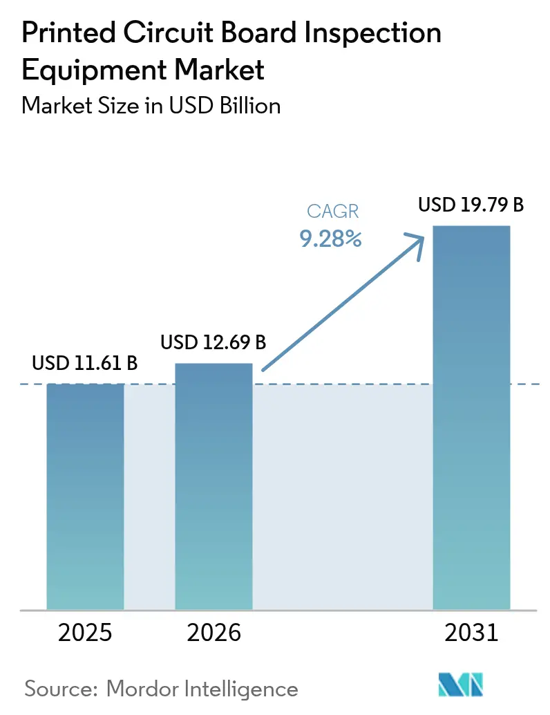
| Market Size (2026) | USD 12.69 Billion |
| Market Size (2031) | USD 19.79 Billion |
| Growth Rate (2026 - 2031) | 9.28 % |
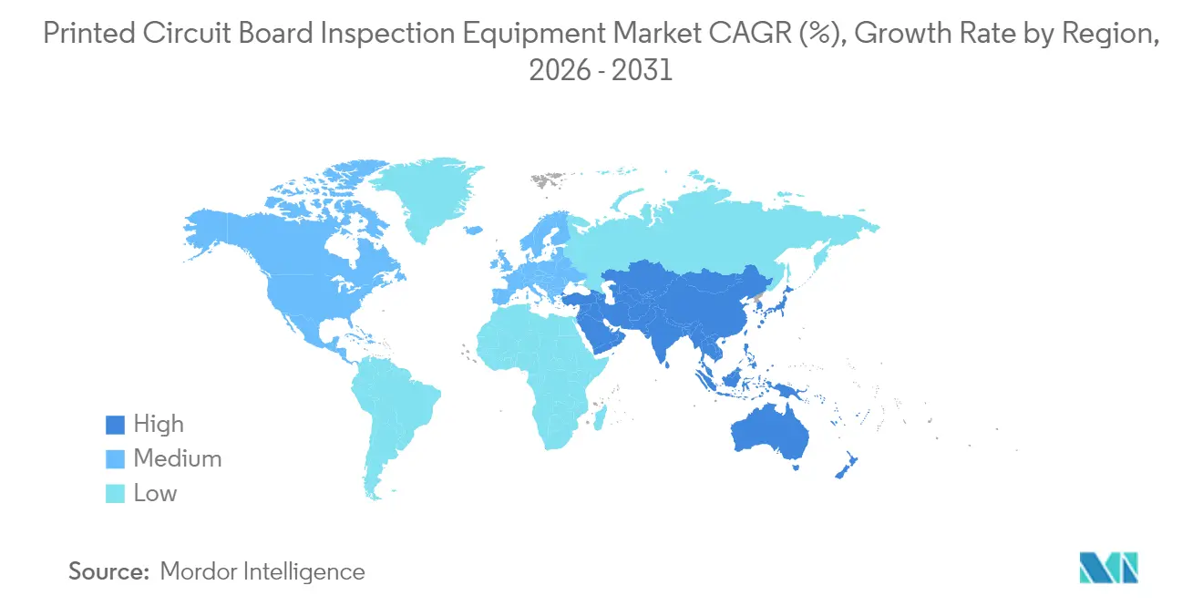
| Fastest Growing Market | Asia Pacific |
| Largest Market | Asia Pacific |
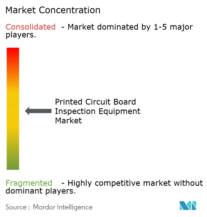
| Market Concentration | Medium |
Major Players *Disclaimer: Major Players sorted in no particular order Image © Mordor Intelligence. Reuse requires attribution under CC BY 4.0. | |
Printed Circuit Board Inspection Equipment Market Analysis by Mordor Intelligence
printed circuit board inspection equipment market size in 2026 is estimated at USD 12.69 billion, growing from 2025 value of USD 11.61 billion with 2031 projections showing USD 19.79 billion, growing at 9.28% CAGR over 2026-2031. Rapid miniaturization, zero-defect mandates in automotive and medical electronics, and sub-micron tolerance requirements in advanced packaging are reshaping investment priorities. Inline automatic optical inspection (AOI) platforms dominate current demand, yet 3D AOI and 3D X-ray systems are accelerating because volumetric imaging, coplanarity measurement, and micro-void detection are now essential for high-density interconnect and chiplet substrates. Electronics manufacturers are also shifting toward pay-per-inspection service models that align equipment costs with throughput, while artificial-intelligence-enabled defect classification reduces false calls and lifts effective capacity. Asia-Pacific leads revenue generation, and automotive electronics is the quickest-expanding end-user segment as electric vehicles (EVs) add USD 1,500-2,000 of electronic content per unit.
Key Report Takeaways
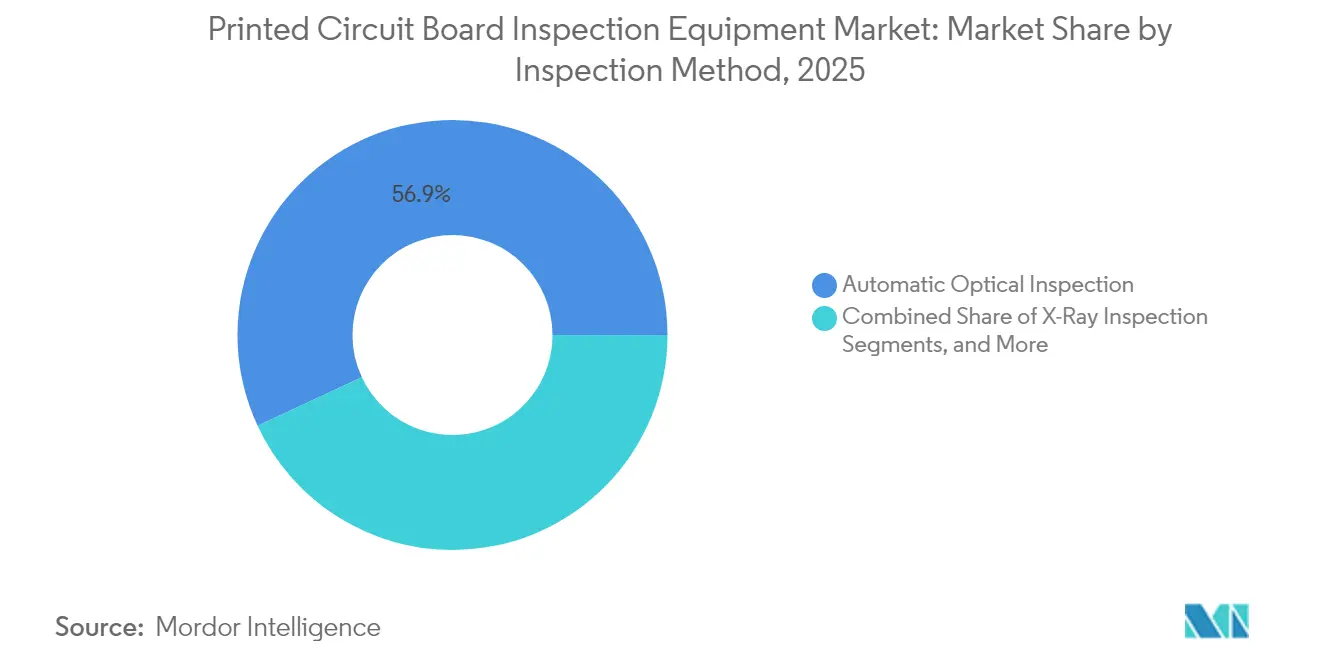
- By inspection method, automatic optical inspection held 56.93% of 2025 revenue; X-ray inspection is poised for the fastest growth with an 10.74% CAGR through 2031.
- By system type, inline platforms led with 60.72% share in 2025, while their own segment also records the highest forecast CAGR at 11.68% to 2031.
- By technology, 2D AOI accounted for 48.02% of 2025 sales; 3D AOI is the quickest-growing technology with a 10.03% CAGR to 2031.
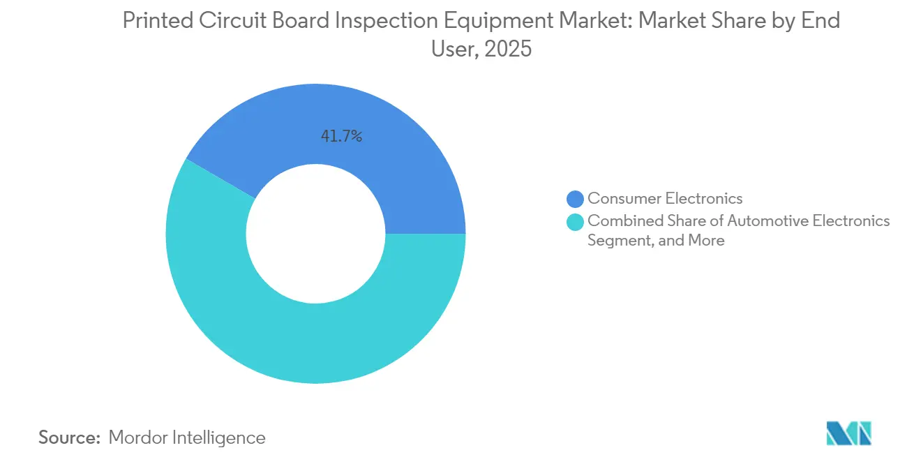
- By end user, consumer electronics contributed 41.65% of demand in 2025; automotive electronics is rising most rapidly at a 9.72% CAGR through 2031.
- By PCB type, rigid boards captured 51.74% of value in 2025; high-density interconnect boards are expanding at a 10.24% CAGR to 2031.
- By geography, Asia-Pacific generated 37.88% of global revenue in 2025 and is advancing at an 11.12% CAGR, the fastest regional pace to 2031.
Note: Market size and forecast figures in this report are generated using Mordor Intelligence’s proprietary estimation framework, updated with the latest available data and insights as of 2026.
Market Trends and Insights
Drivers Impact Analysis of Printed Circuit Board Inspection Equipment Market*
| Driver | (~) % Impact on CAGR Forecast | Geographic Relevance | Impact Timeline |
|---|---|---|---|
| Increasing Miniaturization and Higher Component Densities in Electronics | +2.10% | Global, with APAC core and spill-over to North America | Medium term (2-4 years) |
| Rising Adoption of Industry 4.0 Smart Manufacturing Lines | +1.80% | Global, early gains in Germany, Japan, South Korea | Short term (≤ 2 years) |
| Growth in Automotive Electronics and Electric Vehicles | +2.30% | North America, Europe, APAC automotive hubs | Long term (≥ 4 years) |
| Deployment of Advanced AI-Enabled Defect Classification Reducing False Calls | +1.60% | Global, with early adoption in Taiwan, China, United States | Short term (≤ 2 years) |
| Pay-Per-Inspection and Equipment-as-a-Service Business Models Lowering CapEx Barriers | +1.20% | Global, strongest uptake in North America and Europe | Medium term (2-4 years) |
| Demand for Sub-Micron 3D Inspection in Advanced Packaging and Chiplet PCBs | +1.50% | APAC core (Taiwan, South Korea), spill-over to United States | Long term (≥ 4 years) |
| Source: Mordor Intelligence | |||
Increasing Miniaturization and Higher Component Densities in Electronics
Component pitch in smartphones has already tightened to 0.3 mm, forcing manufacturers to retire manual visual checks in favour of AOI systems able to resolve features below 20 µm. Microvias between 50 µm and 150 µm, blind or buried via stacks, and copper pillars beneath redistribution layers are invisible to 2D grayscale imaging.
Taiwan’s Industrial Technology Research Institute demonstrated a deep-UV 20 nm-resolution prototype in 2024 that identifies micro-cracks in chiplet substrates.[1]Industrial Technology Research Institute, “20-Nanometer Resolution AOI Prototype,” itri.org.tw As a single defect on a USD 5,000 data-center GPU substrate now drives scrap cost, inline 3D inspection at 15 s per board is economically justified.
Growth in Automotive Electronics and Electric Vehicles
Global EV output climbed to 14 million units in 2024 and is expected to surpass 40 million units by 2030. Each EV integrates power modules, battery-management boards, and driver-assistance controllers that collectively triple PCB content versus internal-combustion vehicles.
Tier-1 suppliers have moved to 100% inline X-ray inspection to meet IATF 16949 reliability standards, while ISO 26262 mandates electronic traceability of inspection results for safety-related assemblies.[2]International Organization for Standardization, “ISO 26262: Road Vehicles – Functional Safety,” iso.org Increased inspection intensity lifts demand for both 3D AOI and 3D computed tomography (CT) platforms.
Rising Adoption of Industry 4.0 Smart Manufacturing Lines
Closed-loop feedback systems are transforming electronics manufacturing by tightly integrating solder-paste inspection (SPI), automated optical inspection (AOI), and reflow ovens into a single data-driven workflow. In these next-generation lines, OPC UA serves as the common communication layer, allowing machines from different vendors to exchange defect locations, process parameters, and quality metrics within a few hundred milliseconds. This rapid, standardized data flow enables inspection stations to act immediately on what they detect sending precise coordinate-level feedback to printers or placement machines so they can adjust pressure, alignment, or stencil parameters before small deviations turn into systemic defects.
A 2024 Fraunhofer case study illustrates the impact: automotive manufacturers using real-time SPI-to-printer feedback saw a 42% reduction in solder-related defects and achieved changeovers 30% faster because operator interventions were replaced by automated parameter tuning. Instead of inspection equipment functioning solely as a pass/fail checkpoint, it becomes an active process optimizer that continuously corrects upstream variations.
Deployment of Advanced AI-Enabled Defect Classification Reducing False Calls
Convolutional neural networks (CNNs) are reshaping automated inspection by learning visual patterns directly from large, diverse (“ensemble”) image sets rather than relying on manually tuned rules. By training on varied examples of each defect type different board designs, lighting conditions, solder volumes, and pad geometries these models generalize far better than traditional rule-based vision systems. In practice, they are reaching classification accuracies around 95% and reducing false calls by as much as 40%, a shift that meaningfully improves both quality and line efficiency.
Toolkits such as NVIDIA’s TAO Toolkit make this approach more accessible to manufacturing teams. With transfer learning and pre-trained base models, plants can fine-tune an inspector-specific network using relatively small datasets on the order of a few hundred images per defect class rather than collecting tens of thousands from scratch. This drastically shortens the deployment cycle: what once required months of data curation, labeling, and model engineering can now be completed in weeks, often without deep in-house AI expertise.
Restraints Impact Analysis of Printed Circuit Board Inspection Equipment Market*
| Restraint | (~) % Impact on CAGR Forecast | Geographic Relevance | Impact Timeline |
|---|---|---|---|
| High Initial Capital Investments for Advanced AOI and AXI Systems | -1.40% | Global, acute in emerging markets and small-to-medium enterprises | Short term (≤ 2 years) |
| Shortage of Skilled Technicians for System Programming and Maintenance | -0.90% | Global, most severe in North America and Europe | Medium term (2-4 years) |
| Rapid Technology Obsolescence Leading to Compressed ROI Cycles | -0.70% | Global, particularly impacting early adopters | Medium term (2-4 years) |
| Radiation Safety Compliance Costs for High-Power X-Ray Inspection Lines | -0.50% | Global, stringent in Europe and North America | Long term (≥ 4 years) |
| Source: Mordor Intelligence | |||
High Initial Capital Investments for Advanced AOI And AXI System
Prices for a laser-triangulation 3D AOI platform range from USD 150,000 to 400,000, whereas a sub-micron CT X-ray system commands a price tag exceeding USD 600,000. These high costs pose significant challenges for companies, particularly those operating in cost-sensitive markets, as they require substantial upfront investments. Between 2022 and 2024, rising interest rates pushed the weighted average cost of capital up by 150 to 200 basis points, further straining financial resources by elongating payback periods and causing delays in equipment orders.[3]International Monetary Fund, “World Economic Outlook 2024,” imf.org This financial pressure has led many businesses to reassess their capital allocation strategies. While equipment-as-a-service offerings transform capital expenditure into operational expenditure (OPEX), enabling companies to reduce initial financial burdens, their adoption remains largely confined to mature economies. This limited uptake is attributed to factors such as the availability of advanced infrastructure, favorable regulatory environments, and higher levels of technological readiness in these regions.
Shortage Of Skilled Technicians for System Programming and Maintenance
According to SEMI's 2024 workforce survey, 62% of electronics plants in North America and Europe grapple with inspection-technician vacancies, with these positions remaining unfilled for an average of 120 days. This shortage highlights a critical gap in the availability of skilled labor necessary for maintaining operational efficiency in the electronics manufacturing industry. While AI has streamlined the rule-writing process, it has not eliminated the need for human expertise. Tasks such as model validation, continuous learning, and hardware calibration still require specialized skills that are not easily replaceable.[4]SEMI, “Workforce Survey 2024,” semi.org
The lack of qualified personnel for these roles can significantly impact production timelines, as the onboarding and training of new talent often take considerable time. Consequently, this reliance on specialized talent can prolong ramp-up timelines for new production lines by as much as 12 months, posing challenges for manufacturers aiming to scale operations or introduce new technologies efficiently.
*Our forecasts treat driver/restraint impacts as directional, not additive. The impact forecasts reflect baseline growth, mix effects, and variable interactions.
Printed Circuit Board Inspection Equipment Market Segment Analysis
By Inspection Method:
X-Ray Systems Move Ahead on Hidden JointsAutomatic optical inspection delivered 56.93% of 2025 revenue, demonstrating the breadth of tasks addressable by 2D and emerging 3D optics. X-ray inspection, however, is forecast to expand at an 10.74% CAGR through 2031 as ball-grid arrays, QFNs, and SiP modules proliferate. Computed-tomography units visualize voiding in micro-bumps and through-silicon vias at 1 µm voxel resolution, replacing destructive cross-sectioning. Optical-only stations remain cost-effective for components above 0.5 mm pitch, but their addressable share will narrow as 0.3 mm pitch becomes mainstream. Solder-paste inspection is fully integrated into surface-mount lines to catch stencil defects early, reducing downstream rework by more than 80%.
X-ray adoption draws support from semiconductor packaging trends that push chiplet architectures onto PCB assembly floors. Vendors such as Comet and Waygate now offer CT scanners tailored for high-throughput board lines, merging semiconductor-class resolution with conveyorized handling. Optical stations still dominate low-risk consumer products, yet even in smartphones volumetric checks are rising for under-display cameras and folded flex tails. Overall, x-ray growth lifts the printed circuit board inspection equipment market by unlocking inspection windows unreachable by visible light.


By System Type:
Inline Platforms Capture Throughput EconomicsInline systems held 60.72% of 2025 demand and are projected to progress at a 11.68% CAGR, the fastest among all form factors. Their conveyor integration enables 100% board coverage at 15-30 s per piece without interrupting flow. Closed-loop feedback with printers and placement machines converts defect detection into immediate process correction, a capability that offline stations cannot match. Pay-per-inspection agreements further tilt economics toward inline purchases by treating inspection as a variable cost tied to low volume.
Offline and benchtop stations continue to serve engineering labs, first-article inspections, and low-volume medical, and avionics builds where flexibility outweighs speed. Yet their installed base is slowly declining as contract manufacturers consolidate multiple tasks into single inline nodes. The printed circuit board inspection equipment market therefore leans on inline platforms not only for scale but also for data granularity needed in smart-factory environments.
By Technology:
3D AOI Surges on Coplanarity ControlTwo-dimensional AOI generated 48.02% of 2025 revenue because grayscale algorithms are mature and inexpensive. Three-dimensional AOI is forecast to grow at a 10.03% CAGR, driven by laser-triangulation and structured-light modules that measure height and volume to ±5 µm. The International Electrotechnical Commission released IPC-9716 in 2024, standardizing test patterns and benchmark metrics that confirm 30-40% lower false-call rates when 3D data feed convolutional neural networks.
3D X-ray (CT) complements 3D AOI by exposing hidden voids and through-vias that optical paths cannot see. Although CT carries premium pricing, producers of chiplet-based accelerators and high-bandwidth memory stacks accept the cost because a single escaped defect can scrap USD 5,000 in materials. Consequently, 3D modalities add depth to the printed circuit board inspection equipment market’s value proposition and expand its addressable spend beyond legacy 2D solutions.
By End User:
Automotive Electronics Accelerates on EV UptakeConsumer electronics accounted for 41.65% of the 2025 value, led by smartphones, tablets, and wearables produced in Asia-Pacific mega-factories. Automotive electronics is rising faster, with a 9.72% CAGR, as EV battery packs, traction inverters, and power-distribution units raise PCB count per vehicle. Zero-defect policies and ISO 26262 traceability rules compel tier-1 suppliers to adopt 100% inspection, increasing unit demand for both AOI and CT X-ray.
Industrial and energy electronics use AOI to guarantee 15-20-year reliability of inverters and grid converters. Aerospace and defense segments rely on offline CT and acoustic microscopy for root-cause analysis under AS9100 standards. Medical device makers follow FDA 21 CFR 820 rules, favouring documented calibration and traceability over high throughput. These sectors collectively balance the printed circuit board inspection equipment market by diversifying demand beyond high-volume consumer products.
By PCB Type:
HDI Boards Drive 3D AdoptionRigid PCBs captured 51.74% of 2025 revenue due to broad use in automotive and industrial applications. High-density interconnect (HDI) boards, however, are growing at a 10.24% CAGR. Their microvias, stacked vias, and thin copper features are impossible to validate with 2D grayscale alone, making 3D AOI essential. A 2024 IEEE study showed 65% fewer defect escapes in 0.3 mm-pitch assemblies when 3D AOI replaced 2D algorithms.
Flexible and rigid-flex boards support foldable phones, wearables, and avionics but introduce inspection challenges because transparent substrates and curved geometries create reflection artifacts. Vendors now offer adaptive lighting and bending fixtures to counter these issues. Advanced packaging substrates for chiplets require 1 µm CT scans, a niche covered by a handful of suppliers. Collectively, emerging board types add high-margin volume to the printed circuit board inspection equipment market by demanding multimodal inspection in a single line.
Geography Analysis
APAC Printed Circuit Board Inspection Equipment Market
Asia-Pacific delivered 37.88% of global revenue in 2025 and is expected to expand at an 11.12% CAGR to 2031. China alone accounts for 28% of worldwide electronics manufacturing and hosts contract assemblers such as Foxconn and Luxshare Precision that mandate inline AOI across smartphone, laptop, and wearable lines. South Korea and Taiwan specialize in HDI substrates for memory modules and data-center accelerators, while Japan maintains a premium niche in automotive and industrial electronics that justifies early adoption of CT inspection. Government programs like China’s Made in China 2025 and South Korea’s K-Semiconductor Strategy subsidize smart-factory tools, further lifting regional demand.
North America and Europe Printed Circuit Board Inspection Equipment Market
North America and Europe jointly held roughly 44.62% of 2025 turnover. The United States CHIPS and Science Act allocate USD 52 billion for semiconductor and advanced-packaging plants, many of which will source inspection equipment for substrate and interposer lines. Germany, France, and Italy are upgrading automotive electronics capacity, installing CT X-ray to safeguard battery-pack and power-module quality. Regulatory regimes such as FDA 21 CFR 820 for medical devices and AS9100 for aerospace secure a baseline of offline CT and acoustic microscopy sales.
MEA and South America Printed Circuit Board Inspection Equipment Market
The Middle East, Africa, and South America contribute smaller shares but demonstrate patchy growth. Israel’s defense and medical-device sector insist on IPC Class 3 traceability, prompting CT purchases. Saudi Arabia and the United Arab Emirates have launched domestic electronics programs as part of diversification agendas, adding mid-tier AOI demand. Brazil and Argentina assemble consumer electronics and industrial controls for regional consumption, favouring cost-competitive 2D AOI units yet gradually incorporating Industry 4.0 data collection. These emerging hubs collectively enlarge the printed circuit board inspection equipment market footprint beyond traditional strongholds.

Regulatory Landscape
Inspection equipment procurement is increasingly shaped by industry standards for quality management, traceability, and machine connectivity across end-user verticals. Automotive electronics manufacturing commonly aligns inspection documentation with IATF 16949 and functional-safety traceability requirements under ISO 26262, while medical-device and aerospace builds emphasize documented controls under ISO 13485/EU MDR-aligned quality systems and AS9100 practices. In electronics-specific standardization, IPC standards anchor inspection process control and data exchange, including IPC-9716 for AOI process control and benchmarking, IPC-2591 (IPC-CFX) for machine-to-machine communication across SPI/AOI/AXI nodes, and IPC-OI-645 for visual optical inspection aid requirements and certification provisions.
Recent formal standard activity reinforces the shift toward intelligent, software-defined inspection and consistent defect classification. ITU-T approved Recommendation F.747.16 in March 2025 for 3D machine-vision-based surface defect detection service requirements, and China released multiple national standards relevant to automated defect detection and quality assessment, including GB/T 45575-2025 for industrial product surface defect automatic detection systems (covering deep neural network-based architectures) and GB/T 33772.3-2025 for quality assessment systems for printed boards (published December 2025, effective July 1, 2026). In February 2026, SAC issued GB/T 47234-2026 on general technical requirements for intellectualization of measurement and control equipment, effective September 1, 2026, supporting plant-level moves toward connected, data-rich inspection tools and raising the compliance bar for equipment software, data handling, and integration capabilities.
Competitive Landscape
The top five equipment vendors hold roughly 45% combined revenue, giving the market a moderate concentration. Nordson, Koh Young, and Omron leverage extensive service networks and bundled solutions that link printers, AOI, and reflow ovens. KLA and Camtek migrate semiconductor CT platforms into board assembly, offering 1 µm voxel resolution that addresses chiplet substrates. Regional specialists ViTrox, Mirtec, and Saki provide rapid customization and localized support that resonate with contract manufacturers on thin margins.
AI-enabled defect classification is the dominant competitive theme. Koh Young filed 37 deep-learning patents in 2024 for edge inference at 60 fps. Nordson’s YESTech Orion 3D AOI launched in March 2025 with NVIDIA Jetson Orin, lowering false calls by 35%. Disruptors Pemtron and Unicomp open their software stacks, allowing customers to train propriety neural networks via transfer learning, thereby reducing vendor lock-in. Price competition intensifies in mature 2D AOI after the release of IPC-9716 test metrics that make performance comparisons transparent.
Equipment-as-a-service and cloud analytics emerge as differentiators. Viscom now offers subscription pricing that converts CapEx into OPEX and aligns cash flow with board volume. Predictive-maintenance algorithms bundled into CT systems forecast X-ray tube wear and reduce unplanned downtime. Such service-centric models create recurring revenue for suppliers and raise switching costs, enhancing customer retention while widening the printed circuit board inspection equipment market opportunity.
Printed Circuit Board Inspection Equipment Industry Leaders
Nordson YESTECH Inc
Cognex Corporation
Vision Engineering Inc.
ViTrox Corp Bhd
Omron Electronics LLC
- *Disclaimer: Major Players sorted in no particular order
Printed Circuit Board Inspection Equipment Market Companies Covered in this Report
- Nordson Corporation
- Koh Young Technology Inc.
- Omron Corporation
- ViTrox Corporation Berhad
- Mirtec Co., Ltd.
- Viscom AG
- Saki Corporation
- CyberOptics Corporation
- Test Research Inc.
- KLA Corporation
- Camtek Ltd.
- Yamaha Motor Co., Ltd. (Yamaha SMT)
- Unicomp Technology Co., Ltd.
- Nikon Corporation
- Comet Yxlon GmbH
- Waygate Technologies GmbH
- Shenzhen JT Automation Equipment Co., Ltd.
- GÖPEL electronic GmbH
- Machine Vision Products Inc.
- Pemtron Corporation
Read Analysis of Printed Circuit Board Inspection Equipment Companies

Market Opportunities and Future Outlook
AI server, HPC, and advanced packaging build-outs are creating an opportunity for higher-resolution, higher-throughput inspection on large, high-density boards and substrates where rule-based AOI struggles. In 2026, Machvision cited record monthly revenue tied to demand from AI server/HPC and advanced packaging inspection applications, and OKI reported deployments of AI-based inspection that reduced post-AOI manual visual checks for large, high-density PCBs by about 80%. Together, these examples point to a concrete whitespace in combining 3D data (coplanarity, volume, voiding) with AI classification to reduce false calls and rework, while keeping inline cycle times aligned with high-mix production.
A second opportunity is centered on autonomous inspection and line-level connectivity as manufacturers address technician shortages and pursue closed-loop quality control. ASYS Group presented AISPECTURE at PCIM Europe 2026 as an unsupervised inspection concept, and PEMTRON highlighted connected inspection across SPI, AOI, AXI, and coating inspection for real-time process guidance at SMTA Queretaro in July 2026. With IPC-2591 (IPC-CFX) and common line interfaces used to exchange defect and process data across equipment, vendors that bundle inspection with standardized connectivity, model management, and service-centric delivery (including pay-per-inspection) can target demand from automotive and other regulated end users that require auditable traceability while scaling smart-factory operations across multiple plants.
Recent Industry Developments in Printed Circuit Board Inspection Equipment Market
- May 2026: Cognex launched the In-Sight 3900 Vision System built on Qualcomm Dragonwing platforms to bring embedded, high-speed edge AI to inspection and vision applications. The release is aimed at electronics manufacturers pursuing lower-latency defect detection without relying on external PCs, which helps standardize inspection performance across distributed lines.
- March 2025: Nordson Corporation launched the YESTech Orion 3D AOI with NVIDIA Jetson Orin, enabling real-time classification at 60 fps and reducing false calls by 35%. This reinforced the competitive shift toward AI-accelerated inline AOI for higher-density assemblies where traditional rule-based tuning limits throughput.
- December 2024: ViTrox unveiled the V810 Ultra 3D AOI with 5 micrometer height resolution and positioned it at a price point about 25% below peer offerings. The combination of 3D metrology and more aggressive pricing broadened access to volumetric inspection for HDI and miniaturized PCB applications.


Printed Circuit Board Inspection Equipment Market Report Scope and Research Methodology
Market Definition and Coverage
This market covers equipment used to find, classify, and verify defects on printed circuit boards during manufacturing, before boards move to final assembly. Revenue is counted in USD for inspection systems sold into electronics production lines, including inline and offline installations.
Scope exclusions: It does not count general-purpose factory vision cameras and software unless they are sold as dedicated PCB inspection equipment.
Segments Covered in This Report
- By Inspection Method
- Automatic Optical Inspection (AOI)
- X-Ray Inspection (AXI)
- Solder Paste Inspection (SPI)
- Other Specialized Methods (Acoustic, Laser, Thermography)
- By System Type
- Inline Systems
- Offline / Benchtop Systems
- By Technology
- 2D AOI
- 3D AOI
- 2D X-Ray
- 3D / CT X-Ray
- By End User
- Consumer Electronics Manufacturers
- Automotive Electronics Manufacturers
- Industrial and Energy Electronics
- Aerospace and Defense
- Medical Device Manufacturers
- By PCB Type
- Rigid PCBs
- Flexible and Rigid-Flex PCBs
- High-Density Interconnect (HDI) PCBs
- Advanced Packaging Substrates
- Geography
- North America
- United States
- Canada
- Mexico
- Europe
- United Kingdom
- Germany
- France
- Italy
- Rest of Europe
- Asia-Pacific
- China
- Japan
- India
- South Korea
- Rest of Asia
- Middle East
- Israel
- Saudi Arabia
- United Arab Emirates
- Turkey
- Rest of Middle East
- Africa
- South Africa
- Egypt
- Rest of Africa
- South America
- Brazil
- Argentina
- Rest of South America
- North America
Data Sources, Market Sizing, and Validation
Desk Research
Desk research was used to map demand signals to where inspection equipment is actually installed, and then to set realistic boundaries around what qualifies as PCB inspection equipment. Public sources helped anchor electronics output and trade flows, such as U.S. Census manufacturing data, UN Comtrade shipment statistics, OECD industry indicators, and World Bank macro series that describe factory investment cycles. We also reviewed standards and technical references from bodies such as IPC, along with peer reviewed papers on inspection accuracy and false-call reduction, since these inputs affect replacement cycles and average selling prices.
Alongside these, we reviewed company annual reports and investor presentations to capture product mix signals, regional revenue exposure, and capex commentary from electronics manufacturing. Where needed, paid subscription databases were used only for company financials, patent lookups, and shipment-level import-export checks to confirm directional trends. Desk sources are not exhaustive, so we used additional documents to cross-check points and resolve definition questions.
Primary Interviews and Surveys
Primary work focused on interviews and short surveys with EMS operators, PCB fabricators, quality engineers, line managers, and component and equipment channel participants. We used these conversations to test assumptions on inspection step counts per line, typical inline versus offline deployment, adoption of 2D versus 3D inspection, and how pricing changes when software and service bundles are added. Because this is a global supply chain, inputs were balanced across APAC-heavy manufacturing hubs, EMEA demand pockets, and the Americas, where high-mix production and reshoring related investments are more frequent.
For respondent coverage, the distribution below reflects fieldwork across company sizes, seniority, and the three main demand geographies.
Distribution of primary research fieldwork respondents
| Company type | Respondent position | Region |
|---|---|---|
| Top tier: 31% | CXOs: 13% | APAC: 46% |
| Mid tier: 49% | Functional/Unit leaders: 42% | EMEA: 29% |
| Smaller Players: 20% | Managers: 45% | Americas: 25% |
Market-Sizing & Forecasting
The main build starts from a top-down reconstruction of the addressable inspection spend by linking electronics manufacturing activity to inspection intensity at key production steps. For each region, we translated PCB and electronics output trends into likely line additions and upgrades, and then applied installation rates for AOI, X-ray, and solder paste inspection. We then used an average selling price range that reflects typical system configurations observed in equipment and channel pricing.
To keep totals practical, we corroborated the top-down estimates with selective bottom-up approximations, such as sampled system pricing from channels, sanity checks on shipment volumes, and revenue banding from public disclosures where available.
Inputs used in the model include electronics production growth, PCB complexity indicators (such as HDI and advanced substrate penetration), the share of inline automation on SMT lines, mix shift from 2D to 3D inspection, and replacement timing tied to throughput, false-call rates, and maintenance. When a data gap appeared, we used a conservative range, tested it with expert feedback, and then narrowed it using neighboring indicators like factory capex cycles and export momentum.
For forecasting, scenario analysis was used because demand swings with cycle-driven electronics output and with step-changes in inspection requirements for automotive and advanced packaging. The scenarios were anchored to primary feedback on equipment budgets, plus expected changes in pricing as inspection functions get bundled into newer platforms.
Data Validation & Update Cycle
Validation is done in layers, so the final number is not driven by one input. We compare model outputs against independent signals such as electronics production indices, trade movement for relevant equipment categories, and reported capacity expansion plans. If variance looks too large for a given region, we investigate whether the mismatch is coming from scope, timing, or pricing assumptions.
Before sign-off, a second analyst reviews the logic, units, and conversions, and the checks are repeated at regional and global totals to catch inconsistencies. Reports are refreshed annually, and interim updates are made when major events occur, such as sharp demand shocks in electronics, meaningful pricing moves, or technology transitions that change inspection step counts. Right before delivery, we do a final pass so clients receive the latest updated view.
Mordor Intelligence's Printed Circuit Board Inspection Equipment Market Sizing Compared With Other Published Estimates
Published market sizes for PCB inspection equipment can vary because each publisher draws the boundary differently and also chooses different timing for what is counted as equipment revenue. Differences show up when one study includes broader testing tools, software services, or adjacent factory vision systems, while another stays closer to dedicated inspection equipment sold into PCB and SMT lines.
By tracking installation rates across key inspection steps and refreshing pricing bands through validation calls, Mordor Intelligence keeps the market tied to dedicated PCB inspection equipment, while excluding loosely defined vision and test items that can inflate totals.
Benchmark comparison
| Source | Market Size | Gaps in Research Methodology |
|---|---|---|
| Mordor Intelligence | USD 12.69 B (2026) | |
| Global Consultancy A | USD 4.43 B (2025) | Uses factory-gate framing and a narrower counted revenue pool, which can understate installed-line driven demand when software bundles and higher-end configurations are treated inconsistently across regions. |
| Industry Publisher B | USD 1.47 B (2024) | Appears to apply a tighter product scope and earlier base year, and the limited clarity on inclusions can leave out parts of inline and advanced 3D inspection equipment that are increasingly purchased for high-density boards. |
The spread is mainly explained by scope boundaries and what gets counted as part of an inspection system sale, along with year timing and pricing logic. Our approach stays repeatable because totals are built from clear demand drivers, then cross-checked with channel pricing and expert feedback before the final number is locked.


Key Questions Answered in the Report
What is the current value of the printed circuit board inspection equipment market?
The market is valued at USD 12.69 billion in 2026.
How fast is the printed circuit board inspection equipment market expected to grow?
It is projected to expand at a 9.28% CAGR, reaching USD 19.79 billion by 2031 over 2026-2031.
Which region leads demand for PCB inspection tools?
Asia-Pacific generated 37.88% of global revenue in 2025 and is forecast to grow the fastest at an 11.12% CAGR through 2031.
Why are 3D AOI systems gaining traction?
3D AOI measures height, coplanarity, and solder-paste volume with micron-level accuracy, reducing defect escapes in HDI and chiplet boards.
What drives inspection demand in automotive electronics?
Electric vehicles add up to USD 2,000 of electronic content per car and require zero-defect reliability, prompting 100% inline inspection.
How are vendors lowering capital barriers for customers?
Pay-per-inspection and equipment-as-a-service models shift costs from CapEx to OPEX, making advanced tools accessible to more manufacturers.
Page last updated on:


 Your data is secure and never sold or shared.


