
Photoresist Market Size and Share
Market Overview
| Study Period | 2021 - 2031 |
|---|---|
| Market Size (2026) | USD 3.24 Billion |
| Market Size (2031) | USD 5.53 Billion |
| Growth Rate (2026 - 2031) | 11.31 % |
| Fastest Growing Market | North America |
| Largest Market | Asia Pacific |
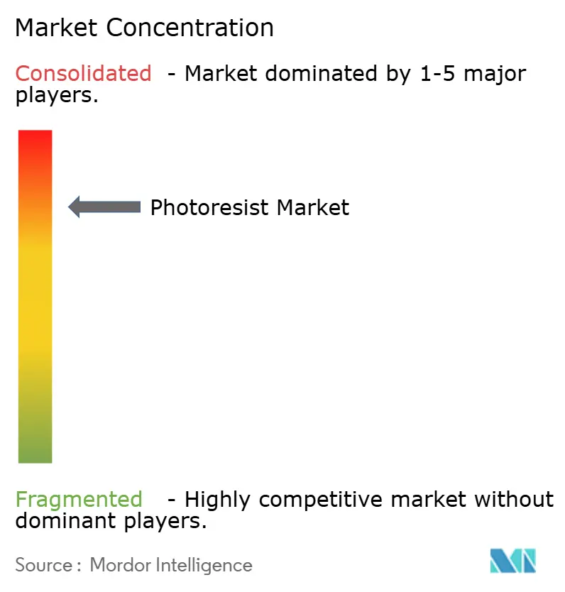
| Market Concentration | High |
Major Players *Disclaimer: Major Players sorted in no particular order Image © Mordor Intelligence. Reuse requires attribution under CC BY 4.0. | |
Photoresist Market Analysis by Mordor Intelligence
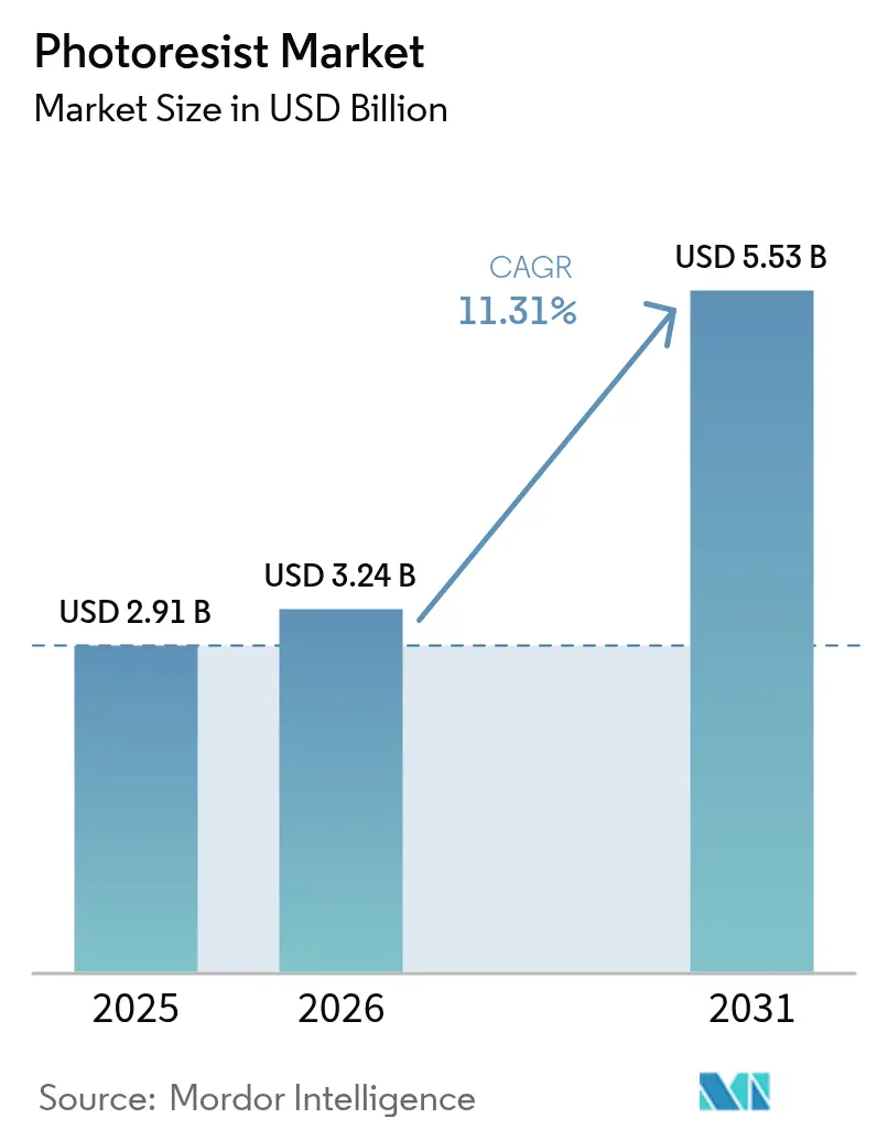
The Photoresist Market size is projected to be USD 2.91 billion in 2025, USD 3.24 billion in 2026, and reach USD 5.53 billion by 2031, growing at a CAGR of 11.31% from 2026 to 2031. Structural shifts underway in semiconductor manufacturing are amplifying demand: extreme-ultraviolet (EUV) lithography is moving from pilot lines to high-volume production, and government-backed fab-localization programs are redrawing supply chains for critical materials such as photoresist. Mature 193-nanometer ArF immersion formulations continue to anchor the cost-optimized nodes used in automotive microcontrollers, but next-generation metal-oxide dry resists are now essential at sub-5-nanometer logic, where photon shot noise and line-edge roughness threaten yield. Supply resilience considerations have also intensified as the U.S. and EU CHIPS Acts channel a significant amount into local wafer-fabrication capacity, compelling resist suppliers to duplicate blending and quality-assurance assets within North America and Europe.
Key Report Takeaways
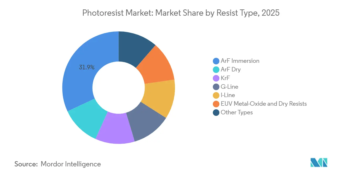
- By resist type, ArF immersion held 31.92% of the Photoresist market share in 2025, whereas EUV metal-oxide and dry resists are projected to expand at a 12.94% CAGR through 2031.
- By tone, positive resists commanded 71.51% revenue share in 2025; negative resists post the fastest 11.38% CAGR to 2031.
- By application, semiconductors and ICs accounted for 54.77% of the Photoresist market size in 2025, while advanced packaging is set to grow at a 11.95% CAGR through 2031.
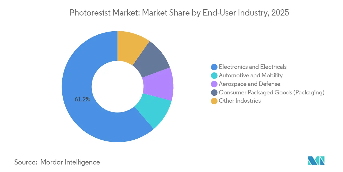
- By end-user industry, electronics and electricals accounted for 61.22% of the market size in 2025, while automotive and mobility are set to grow with the fastest CAGR of 11.86% through 2031.
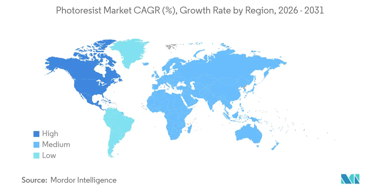
- By geography, the Asia-Pacific held the largest share of 72.34% of the market in 2025. However, North America is expected to witness the fastest growth at a CAGR of 11.49% during the forecast period.
Note: Market size and forecast figures in this report are generated using Mordor Intelligence’s proprietary estimation framework, updated with the latest available data and insights as of 2026.
Global Photoresist Market Trends and Insights
Drivers Impact Analysis*
| Drivers | (~) % Impact on CAGR Forecast | Geographic Relevance | Impact Timeline |
|---|---|---|---|
| Growing demand from semiconductor and AI accelerators | +3.2% | Global, with APAC core and North America acceleration | Medium term (2-4 years) |
| Accelerated EUV lithography adoption and High-NA roadmap | +2.8% | APAC (Taiwan, South Korea), North America (Intel fabs), Europe (IMEC pilot lines) | Long term (≥ 4 years) |
| 5G/IoT proliferation expanding wafer starts | +1.9% | Global, with APAC manufacturing concentration | Medium term (2-4 years) |
| Government fab-incentive programs (US/EU Chips Acts) | +2.4% | North America, Europe, with supply-chain spillover to APAC | Long term (≥ 4 years) |
| Metal-oxide dry-deposited resists boosting EUV throughput | +1.0% | APAC leading-edge fabs, North America pilot lines | Long term (≥ 4 years) |
| Source: Mordor Intelligence | |||
Growing Demand from Semiconductor and AI Accelerators
Worldwide capital expenditure on wafer-fabrication equipment is slated to rise between 2026 and 2028, reflecting heavier AI-accelerator requirements in hyperscale data centers[1]. Alphabet doubled its outlays for tensor-processing units in 2025, raising overlay-tolerance specifications that directly increase photoresist consumption per wafer. Intel’s Lunar Lake processors integrate on-package memory using through-silicon vias, adding specialized redistribution-layer lithography steps that further drive resist intensity. Because advanced chiplet architectures raise the number of masking passes, resist demand is decoupling from smartphone unit cycles, sustaining growth even as handset shipments level off. TSMC locked in multiyear EUV-resist supply agreements for its Arizona fab two years before ramp to guarantee chemistry availability, underscoring the material’s strategic role.
Accelerated EUV Lithography Adoption and High-NA Roadmap
In 2024, ASML rolled out its inaugural 0.55 numerical-aperture High-NA EUV scanner, an innovation that facilitates 8-nanometer half-pitch patterning, sidestepping the expenses of multi-patterning. Intel has pledged allegiance to High-NA for its 18-angstrom node, while Samsung and TSMC eye sub-3-nanometer integration post-2027. High-NA optics grapple with absorption coefficients exceeding 10 µm-¹ at 13.5 nm. This is a challenge zone, as traditional chemically-amplified compositions falter with line-edge roughness. While metal-oxide alternatives, derived from tin-oxo clusters, satisfy absorption criteria, they bring forth stochastic defects. This challenge has spurred a collaborative effort between JSR and Lam Research, aiming to reduce defect density. Their co-optimization strategy forges a closer bond between resist suppliers and tool manufacturers, setting a higher barrier for industry newcomers.
5G/IoT Proliferation Expanding Wafer Starts
Global wafer starts tied to 5G radios and IoT sensors continue to swell as network operators densify small-cell footprints and enterprises instrument factories and logistics assets. KrF and ArF dry resists remain vital here because analog front-ends and microcontrollers sit on cost-sensitive 90- to 28-nanometer nodes that must balance die size and RF performance. Incremental volume from these devices cushions fabs against advanced-node cyclicality. As IoT deployments move from proof-of-concept to scale, the cumulative masking layers surge, extending demand momentum into the medium term.
Government Fab-Incentive Programs (US/EU CHIPS Acts)
Under the U.S. CHIPS and Science Act, TSMC received funding, Intel got funding, Samsung was awarded funding, and Micron secured funding, all while backing private investments. Meanwhile, Europe, through its Chips Act, mobilized funding, designating funding for Intel's project in Magdeburg and funding for a joint fabrication facility by STMicroelectronics and GlobalFoundries. The terms of these subsidies emphasize local material content. As a result, Tokyo Ohka Kogyo established a technical center in Oregon, and Merck KGaA expanded its campus in Arizona. Such developments disrupt the previously Asia-dominated resist supply chain, introducing regional bottlenecks and complicating qualification processes.
Restraints Impact Analysis*
| Restraints | (~) % Impact on CAGR Forecast | Geographic Relevance | Impact Timeline |
|---|---|---|---|
| Stringent HSE rules on solvents and photo-acid generators | -0.9% | Global, with EU REACH and U.S. EPA enforcement leading, spillover to APAC manufacturing | Short term (≤ 2 years) |
| Supply-chain concentration and export-control exposure | -0.7% | APAC supply base (Japan, South Korea), North America and EU demand centers, China isolated markets | Medium term (2-4 years) |
| Yield risk from stochastic defects in sub-10 nm patterning | -0.8% | APAC leading-edge fabs (Taiwan, South Korea), North America High-NA pilot lines | Long term (≥ 4 years) |
| Source: Mordor Intelligence | |||
Stringent HSE Rules on Solvents and Photo-Acid Generators
The U.S. EPA classified several PFAS solvent families as hazardous in 2024, mandating costly abatement or substitution at resist-blending plants within two years[2]. The EU added triphenylsulfonium salts to its REACH authorization list in 2025, imposing sunset dates that accelerate reformulation campaigns and tilt research and development budgets away from high-performance chemistry toward compliance work[3]. Tokyo Ohka Kogyo disclosed that a significant amount of its 2025 research and development spend was consumed by solvent reformulations, reinforcing a trend where only the largest suppliers can carry simultaneous compliance and node-transition programs. Industry lobbying secured a five-year carve-out for EUV resists, yet environmental-advocacy lawsuits threaten to shorten the grace period, injecting regulatory uncertainty into capacity-planning models.
Supply-Chain Concentration and Export-Control Exposure
Japan's top suppliers dominate ArF and EUV chemistries. This geographic monopoly came to light in 2024 when the U.S. added specific precursors to its Entity List, halting shipments to Chinese fabs operating at 14-nanometer and smaller. In response, China rolled out subsidies for local producers like Jiangsu Nata. However, these domestic materials lag behind their Japanese counterparts in terms of defect density. Now, fabs face a dilemma: they can either dual-source, incurring extra metrology and inventory costs, or shift procurement closer to U.S. or EU lines to tap into available incentives. Resist vendors are at a crossroads: they can either establish manufacturing in multiple regions or lose market share in areas where export regulations render supply unfeasible.
*Our forecasts treat driver/restraint impacts as directional, not additive. The impact forecasts reflect baseline growth, mix effects, and variable interactions.
Segment Analysis
By Resist Type: Metal-Oxide Chemistries Redefine EUV Economics
ArF immersion held 31.92% of the photoresist market share in 2025, while EUV metal-oxide and dry resists are forecast to expand at a 12.94% CAGR, capturing incremental photoresist market size from sub-5-nanometer logic nodes.
Chemically amplified ArF immersion remains the price-performance leader for 28- to 7-nanometer automotive and connectivity chips, delivering solid yields on fully-depreciated scanners. KrF, g-line, and i-line formulations persist in analog and MEMS lines, buffering suppliers against EUV-cycle volatility. Conversely, tin- and hafnium-based metal-oxide systems enable the High-NA EUV roadmap with 2-nm line-edge roughness performance, albeit at higher exposure dose and cost. Toolmakers and chemistry suppliers are co-designing deposition-etch sequences that promise to cut cycle time, which, if realized at scale, could swing total cost of ownership toward metal-oxide in the outer years of the forecast.

By Tone: Negative Resists Gain in Double-Patterning Schemes
Positive-tone chemistries commanded 71.51% share in 2025, yet negative-tone resists are climbing at an 11.38% CAGR, driven by their robustness in self-aligned double-patterning and EUV contact layers.
Advanced packaging flows favor the thicker films and aqueous developers of positive-tone materials, but sub-7-nanometer logic increasingly uses negative-tone for via layers that would otherwise collapse under rinse stress. Suppliers are releasing switchable-tone hybrids that toggle through bake-temperature adjustments, allowing fabs to maintain a single base chemistry across multiple layers and dilute qualification overhead, thereby augmenting photoresist market size gains from tone diversification.
By Application: Advanced Packaging Outpaces Logic and Memory
Semiconductors and ICs held a 54.77% share, yet advanced packaging is advancing at an 11.95% CAGR, underscoring a pivot from pure scaling to heterogeneous integration.
Fan-out wafer-level packaging and chip-on-wafer stacks use 2-µm redistribution lines that require triple masking passes compared with wire-bond flows. TSMC’s CoWoS platform and Intel’s Foveros 3D stacking both hike resist layers per finished device, inflating photoresist market size beyond what front-end volume alone would imply. Flat-panel displays and printed-circuit boards remain mid-teen contributors, while MEMS, sensors, and photomasks offer niche but fast-evolving formulation requirements that diversify supplier revenue.
By End-User Industry: Automotive Electrification Accelerates Chip Intensity
Electronics and electricals accounted for 61.22% of demand in 2025, although automotive and mobility are forecast to log an 11.86% CAGR through 2031 as vehicle semiconductor content climbs.
Powertrain electrification and driver-assistance radars rely on 180- to 28-nm nodes that remain on mature exposure tools but add masking layers for redundancy and safety. Infineon reported record automotive revenue in 2025, citing thick-film trench resists for silicon-carbide MOSFETs as a growth vector. Aerospace and defense, though smaller, commands high margins for radiation-tolerant resists, while emerging smart-packaging labels point to future thin-film opportunities.
Geography Analysis
Asia-Pacific captured 72.34% of the photoresist market in 2025. This dominance is largely attributed to Taiwanese and South Korean fabs, which handle the majority of the world's leading-edge wafers. Meanwhile, North America is set to increase its foothold, with an 11.49% CAGR. Thanks to the CHIPS Act, projects in Arizona, Ohio, and Texas are on track to contribute significantly to the global 2- to 5-nm capacity by 2028. This surge is prompting suppliers to establish blending lines closer to their customers.
Europe is experiencing moderate growth, driven by Intel's investment in Magdeburg and a joint venture between STMicroelectronics and GlobalFoundries in France. However, Europe still relies on imports for its EUV resists. China faces challenges due to export controls on advanced photoresists. As a countermeasure, it's aggressively expanding its 28-nm capacity and is heavily investing in ArF dry and KrF chemistries. Yet, the nation grapples with developing its domestic High-NA capability.
India and the Middle East are emerging as significant players in the photoresist landscape. Micron's assembly-test facility in Gujarat and Tata-Powerchip's fab agreement signify India's inaugural moves into wafer fabrication. Concurrently, Abu Dhabi's Mubadala is spearheading a packaging cluster, initially dependent on imported KrF resists. While these developments offer suppliers a chance to diversify away from the Asia-Pacific stronghold, the immediate volume impact is minimal.
Regulatory Landscape
Environmental and chemical-management rules are tightening around solvents, fluorinated additives, and photo-acid generators used in KrF/ArF formulations, which increases compliance and reformulation workloads for resist blenders. The current study window highlights the U.S. EPA classifying several PFAS solvent families as hazardous in 2024 and the EU adding triphenylsulfonium salts to its REACH authorization list in 2025. Both developments push suppliers toward PFAS-free and alternative PAG chemistries while also raising qualification requirements at fabs.
Trade and export-control measures are further reshaping material flows for advanced-node production. In 2026, China Customs introduced a mandatory Restriction Identification Code for exports of KrF/ArF photoresists and IC cleaning solvents, while SEMI flagged tighter controls affecting core monomers used in KrF/ArF supply chains, increasing licensing and documentation burdens. These changes align with CHIPS Act-driven localization programs that emphasize local material content, reinforcing the need for regionally duplicated blending and QA footprints alongside regulatory compliance capabilities.
Value Chain Analysis
The photoresist value chain starts with upstream petrochemical and specialty-chemical inputs, including resins, photoactive compounds (PAGs), sensitizers, and high-purity solvents such as PGME/PGMEA. It then moves through synthesis, formulation and blending, ultra-trace purification, filtration, and clean packaging, with qualified logistics delivering materials into fabs. Multi-month qualification, strict process-change notification (PCN) controls, and defectivity metrology gate any material change, which slows switching feedstocks or suppliers even when shortages emerge.
Recent events point to bottlenecks and concentration risk across the chain. In 2026, disruptions to naphtha availability tightened solvent and precursor supply, and Japanese photoresist suppliers including JSR, Tokyo Ohka Kogyo (TOK), Shin-Etsu Chemical, and FUJIFILM warned major Korean chipmakers of potential disruption, reflecting dependence on a narrow set of high-purity inputs and producers. At the same time, suppliers are adding downstream capability closer to consumption points, such as Asahi Kasei completing a new SUNFORT dry film photoresist slitting facility in Tainan (Taiwan), which expanded capacity by 40%. Industry alerts on export controls for certain monomers also increased lead times, strengthening the case for inventory, licensing, and multi-region qualification strategies.
Competitive Landscape
The Photoresist market is consolidated. DuPont and Merck KGaA are widening portfolios via acquisition, bundling anti-reflective coatings, cleaning chemistries, and resists to simplify fabs’ supply chains. Patent filings for metal-oxide formulations jumped in 2024-2025, with FUJIFILM and Sumitomo entering the race. Equipment vendors may forward-integrate further, a scenario that could commoditize standalone resist supply and compress supplier margins. Meanwhile, stringent solvent regulations are shrinking the viable vendor pool, amplifying the competitive moat for firms with compliance scale.
Photoresist Industry Leaders
-
TOKYO OHKA KOGYO CO., LTD.
-
JSR Corporation
-
FUJIFILM Corporation
-
Shin-Etsu Chemical Co., Ltd.
-
DuPont
- *Disclaimer: Major Players sorted in no particular order
Market Opportunities and Future Outlook
Leading-edge lithography is pulling the market toward higher-value resist platforms and deeper process co-optimization, creating whitespace in EUV and High-NA-ready materials, including metal-oxide resists and dry-deposited approaches that target stochastic defects and line-edge roughness. In 2026, Imec demonstrated oxygen injection during post-exposure bake to improve the dose response of metal-oxide photoresists, and collaborative High-NA EUV patterning demonstrations involving Lam Research, ASML, and Imec showed continued progress on tooling and process integration. Together, these efforts support a pathway for suppliers that can pair chemistry with tool and process integration, rather than selling stand-alone formulations.
Regionalization and compliance-driven substitution are also creating nearer-term commercial lanes beyond pure node scaling. JSR announced plans to build a photoresist manufacturing facility in Taiwan to supply TSMC, and Sumitomo Chemical disclosed plans to add an integrated technology management, quality evaluation, and analysis facility at its Osaka Works, both reflecting the growing burden of qualification and local-content requirements tied to fab incentive programs. In China, capacity additions such as Dinglong bringing KrF/ArF photoresist production to 330 tons per year in 2026 reflect efforts to mitigate export-control exposure, while PFAS and solvent restrictions are accelerating demand for fluorine-free or PFAS-free alternatives, as shown by FUJIFILM and other suppliers. Advanced packaging remains an additional expansion lane, supported by capacity moves like Asahi Kasei expanding dry film photoresist slitting capacity in Taiwan to serve AI server packaging flows that use more lithography steps per finished package.
Recent Industry Developments
- June 2026: Tokyo Ohka Kogyo (TOK) commenced operations at its new Aso Kumamoto Site in Kikuchi City, Kumamoto Prefecture, following an investment of about JPY 13 billion. The start-up adds regional manufacturing presence near a major semiconductor cluster, supporting supply assurance and faster customer qualification cycles for critical lithography materials.
- May 2026: JSR Corporation announced plans to build its first semiconductor materials production facility in Taiwan to supply photoresist directly to TSMC. Establishing in-region production shortens logistics and reduces single-region supply exposure as fabs push for resilient, locally qualified materials tied to expansion programs.
- April 2024: Shin-Etsu Chemical announced it would build a new production base in Japan that will become its fourth production base for semiconductor lithography materials. The added manufacturing footprint strengthens capacity and redundancy for high-purity lithography materials used across advanced and mature nodes.
Research Methodology Framework and Report Scope
Market Definition and Coverage
For this methodology, the photoresist market covers the value of light sensitive resist materials sold for lithography and patterning steps used in semiconductor and related microfabrication workflows, counted at the point of sale by suppliers across end users and regions.
Scope exclusions: It excludes lithography tools and services, and it also excludes adjacent photoresist ancillaries such as developers, strippers, and anti reflective coatings when they are sold as separate product lines.
Segmentation Overview
- By Resist Type
- ArF Immersion
- ArF Dry
- KrF
- G-Line
- I-Line
- EUV Metal-Oxide and Dry Resists
- Other Types
- By Tone
- Positive
- Negative
- By Application
- Semiconductors and ICs
- Advanced Packaging (Fan-Out WLP, RDL)
- Flat-Panel Displays (LCD/OLED)
- Printed Circuit Boards
- MEMS and Sensors
- Other Applications
- By End-User Industry
- Electronics and Electricals
- Automotive and Mobility
- Aerospace and Defense
- Consumer Packaged Goods (Packaging)
- Other Industries
- By Geography
- Asia-Pacific
- China
- Japan
- South Korea
- Taiwan
- India
- Rest of Asia-Pacific
- North America
- United States
- Canada
- Mexico
- Europe
- Germany
- United Kingdom
- France
- Italy
- Russia
- Rest of Europe
- South America
- Brazil
- Argentina
- Rest of South America
- Middle-East and Africa
- Saudi Arabia
- United Arab Emirates
- South Africa
- Rest of Middle-East and Africa
- Asia-Pacific
Data Sources, Market Sizing, and Validation
Desk Research
Desk research starts by building a clear demand map for where photoresist is consumed, then matching that to how material shipments typically move through the semiconductor supply chain. We relied on public industry and government sources such as SEMI capacity and fab outlook publications, World Semiconductor Trade Statistics for device market signals, and trade statistics from agencies such as the USITC and UN Comtrade to cross check chemical import and export flows.
We also used company annual reports and investor presentations, plus selected coverage from business publications, and technical papers from journals and conference proceedings that discuss resist performance shifts (for example, EUV adoption and line edge roughness topics). Patent databases were checked to understand where new resist chemistries were being filed, which helped test whether the growth assumptions were directionally reasonable. In addition, we used paid subscriptions for company financials and intelligence, and for shipment level import and export data where available, to validate the trade signals. These sources are illustrative only, and we reviewed other public documents as well to support data collection, clarification, and cross validation.
Primary Interviews and Surveys
Primary interviews focused on confirming how volume shifts by node migration, where EUV layers are actually being added, and how pricing is negotiated across direct supply and distributors. We spoke with resist formulators, chemical distributors, and semiconductor ecosystem participants (process and procurement roles) across APAC, EMEA, and the Americas, so assumptions from desk research could be corrected before finalizing the model.
Distribution of primary research fieldwork respondents
| Company type | Respondent position | Region |
|---|---|---|
| Top tier: 35% | CXOs: 13% | APAC: 38% |
| Mid tier: 50% | Functional/Unit leaders: 43% | EMEA: 37% |
| Smaller Players: 15% | Managers: 44% | Americas: 25% |
Market-Sizing & Forecasting
Sizing begins with a top-down rebuild of the addressable demand pool by linking wafer capacity and starts, layer intensity, and resist consumption per layer, then converting that into value using typical selling price bands by resist family. To keep the model grounded, we tracked a few consistent fingerprints: announced wafer fab capacity ramps, the share of EUV versus ArF and KrF usage, the typical number of critical layers per device generation, and observed pricing changes tied to purity requirements and yield learning.
After establishing the demand pool, we cross checked it with selective bottom-up approximations using supplier revenue disclosures where available, channel checks on average selling prices, and sanity checks against trade movement of specialty chemicals in major producing and consuming regions. Where direct data was not available for smaller suppliers or niche applications, we filled gaps using proxy shares from similar end uses and then stress tested those shares in interviews. For forecasting, we used scenario analysis, since photoresist demand can shift quickly with fab delays, node transitions, and qualification timing, and we anchored scenarios using consensus expectations shared by industry participants during primary discussions.
Data Validation & Update Cycle
Validation is carried out through repeated cross checks between the model and independent signals, such as semiconductor capex direction, wafer start trends, and announced capacity timelines, with outlier review before totals are finalized. If a region or resist family shows a sudden jump that does not align with capacity additions or pricing logic, we rework the assumptions and trigger follow up calls.
Each report is refreshed annually, and interim updates are made when material events occur, such as large fab start delays, major supply disruptions, or step changes in EUV layer adoption. Before delivery, we run a final pass so clients receive the latest updated view rather than an older snapshot.
Mordor Intelligence's Photoresist Market Sizing Compared With Other Published Estimates
Published market sizes for photoresist can differ substantially, even when they cover similar end uses, because scope boundaries and the pricing arithmetic are not handled the same way across reports. Most gaps trace back to which adjacent chemical categories are included, what base year is treated as the reference, and how fast pricing is assumed to move as EUV adoption expands.
For photoresist specifically, a key driver is whether photoresist ancillaries are counted inside the same total, since developers, removers, and coatings can be bundled in some procurement views. Another driver is how demand is linked to wafer activity, because some estimates place more weight on electronics output value while others rebuild from wafer starts and layer counts, which can change results during node transitions. Currency conversion timing and refresh cadence also affect published outcomes, since specialty chemicals can react to short term pricing and capacity news.
Benchmark comparison
| Source | Market Size | Gaps in Research Methodology |
|---|---|---|
| Mordor Intelligence | USD 2.91 B (2025) | |
| Global Research Publisher A | USD 5.19 B (2025) | This estimate is broader in scope because it segments and counts ancillary types alongside photoresist, and it can also apply a different product mapping that lifts the starting value. |
| Industry Publisher B | USD 4.37 B (2025) | The figure combines photoresist with photoresist ancillaries in one total, which increases the market size relative to a resist-only view and can smooth pricing changes across categories. |
The table shows the spread is mainly explained by whether adjacent process chemicals are folded into the same total and by how wafer activity is translated into dollars. By keeping the count limited to photoresist material sales and by checking the demand build against wafer capacity and layer intensity, the 2025 value stays tied to a narrower demand pool, a modeling choice applied by Mordor Intelligence.
Key Questions Answered in the Report
What is the projected value of the photoresist market in 2031?
It is forecast to reach USD 5.53 billion by 2031, reflecting an 11.31% CAGR from USD 3.24 billion in 2026.
Which region is growing fastest for photoresists?
North America leads with an 11.49% CAGR, supported by CHIPS Act-funded fabs coming online after 2026.
Why are metal-oxide resists significant for future lithography?
They enable High-NA EUV patterning below 5 nm by offering higher photon absorption and better etch selectivity than organic chemistries.
How do environmental regulations affect resist suppliers?
New EPA and REACH rules on PFAS solvents and photo-acid generators force costly reformulation, favoring large vendors with compliance scale.
What factors drive photoresist demand in the automotive sector?
Electric-vehicle powertrain and ADAS chips increase lithography layers per car, pushing automotive resist demand toward an 11.86% CAGR.