
Photodiode Sensors Market Size and Share
Market Overview
| Study Period | 2021 - 2031 |
|---|---|
| Market Size (2026) | USD 0.83 Billion |
| Market Size (2031) | USD 1.16 Billion |
| Growth Rate (2026 - 2031) | 7.12 % |
| Fastest Growing Market | Asia Pacific |
| Largest Market | Middle East and Africa |
| Market Concentration | Medium |
Major Players *Disclaimer: Major Players sorted in no particular order Image © Mordor Intelligence. Reuse requires attribution under CC BY 4.0. | |
Photodiode Sensors Market Analysis by Mordor Intelligence
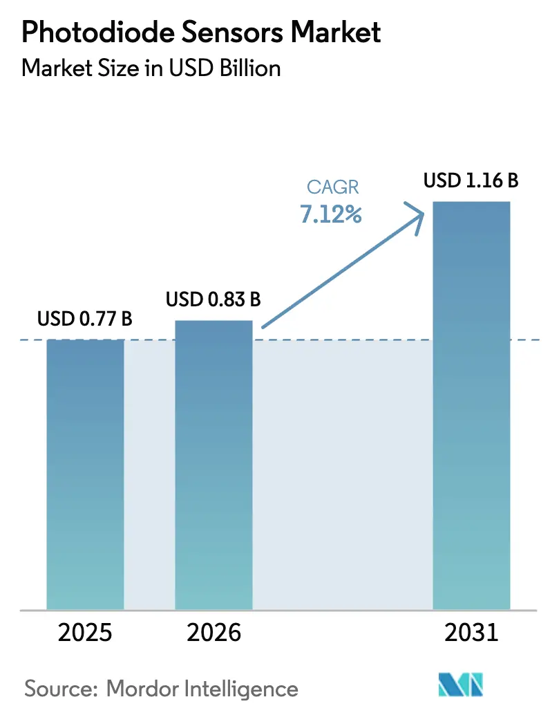
photodiode sensors market size in 2026 is estimated at USD 0.83 billion, growing from 2025 value of USD 0.77 billion with 2031 projections showing USD 1.16 billion, growing at 7.12% CAGR over 2026-2031. Global demand is rising because 5G back-haul, LiDAR-enabled vehicles, and data-center photonics each require precision optical receivers that outperform legacy designs[1]. The photonics sector’s resilience—valued at USD 865 billion in 2022 and forecast to hit USD 1.2 trillion in 2027—further underpins the photodiode sensors market growth trajectory. Supply chain vulnerabilities for indium and gallium, however, introduce cost and lead-time risks that could temper near-term output levels. [2] Competitive differentiation is now shifting from discrete components toward integrated modules that combine photodiodes, signal processing, and packaging in a single unit, shortening customers’ time-to-market in telecommunications, automotive, and medical imaging verticals.
Key Report Takeaways
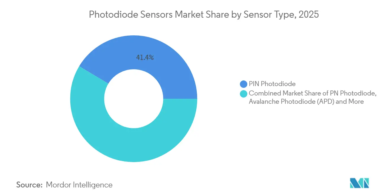
- By sensor type, PIN devices led with 41.42% of the photodiode sensors market share in 2025, while avalanche photodiodes are set to advance at an 8.23% CAGR through 2031.
- By material, silicon captured 57.38% share of the photodiode sensors market size in 2025, whereas silicon-germanium technology is projected to expand at an 8.01% CAGR.
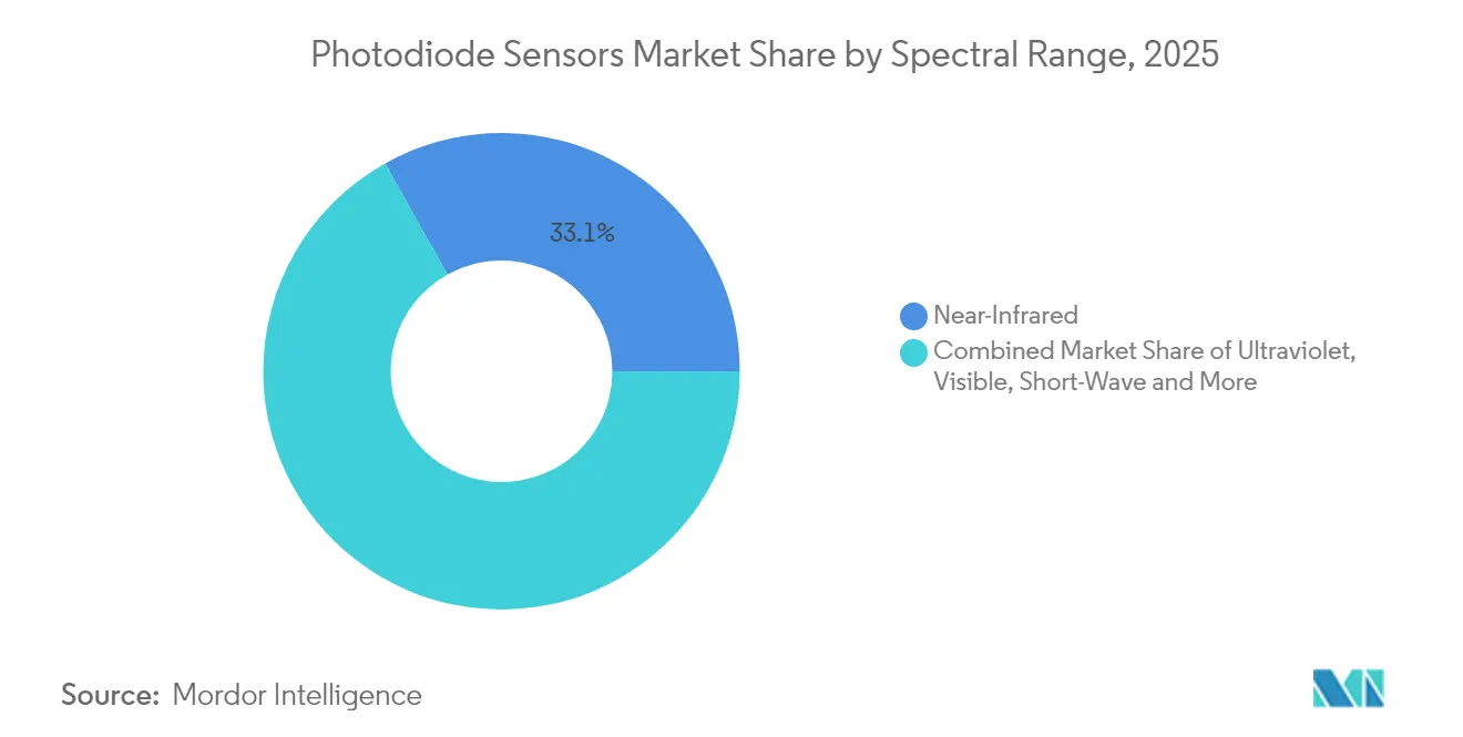
- By spectral range, near-infrared held 33.12% revenue share in 2025; short-wave infrared (SWIR) is the fastest-growing band with an 8.31% CAGR to 2031.
- By end-user industry, consumer electronics accounted for 28.45% of the photodiode sensors market size in 2025, yet automotive LiDAR is forecast to grow at an 8.62% CAGR through 2031.
- By geography, Asia-Pacific dominated at 45.55% share in 2025, whereas the Middle East & Africa region is paced to rise at a 9.22% CAGR from 2026-2031.
Note: Market size and forecast figures in this report are generated using Mordor Intelligence’s proprietary estimation framework, updated with the latest available data and insights as of 2026.
Market Trends and Insights
Drivers Impact Analysis of Photodiode Sensors Market*
| Driver | (~) % Impact on CAGR Forecast | Geographic Relevance | Impact Timeline |
|---|---|---|---|
| Surge in optical-fiber & 5G back-haul deployments | +1.8% | Global (APAC, North America lead) | Medium term (2–4 years) |
| Accelerating LiDAR/ADAS integration in vehicles | +1.5% | North America, Europe, China automotive hubs | Medium term (2–4 years) |
| Smartphone demand for ambient-light & proximity-sensing | +1.2% | Global, concentrated in APAC manufacturing | Short term (≤ 2 years) |
| Expanded use in medical imaging & pulse-oximetry | +0.9% | North America, Europe, emerging APAC markets | Long term (≥ 4 years) |
| Source: Mordor Intelligence | |||
Surge in Optical-Fiber & 5G Back-haul Deployments
Data-heavy 5G networks are pushing operators to upgrade backbone links using coherent optical transceivers that rely on low-noise photodiodes. Trials by NTT and NEC using IOWN All-Photonics Networks demonstrated real-time traffic monitoring over existing fiber, confirming dual-use value for infrastructure owners.[3]Academic prototypes have already moved toward 100 Gbps photodiodes capable of 100-km reach, matching early 6G fronthaul benchmarks. Free-space optical links that hit 36.4 Gbit/s highlight the versatility of high-bandwidth receivers in urban environments where trenches are costly. Power-efficient datacenter interconnects show transmitter-side energy efficiency at 1.59 pJ/bit, putting pressure on detector makers to improve receiver sensitivity at similar power budgets.[4] Combined, these requirements place the photodiode sensors market at the heart of next-generation wireline and wireless convergence strategies.
Accelerating LiDAR/ADAS Integration in Vehicles
LiDAR adoption is moving beyond premium brands as cost curves fall rapidly. Sony’s IMX479 stacked SPAD depth sensor delivers 300-m detection at 37% photon-detection efficiency with sample shipments slated for autumn 2025. Korea’s SPAD roadmap hit 56 ps timing jitter and 8 mm resolution, ideal for short-range driver-assistance systems. Chinese suppliers have spurred price competition, accelerating unit volume growth in mid-range vehicles. VCSEL-to-photodiode co-packaging is cutting bill-of-materials while boosting reliability. FMCW architectures, which depend on heterodyne photodiodes, are now reaching detection limits near theoretical ceilings, validating upcoming production rollouts.[5]
Smartphone Demand for Ambient-Light & Proximity Sensing
Handset makers continue integrating ambient-light, proximity, and PPG biosensing into consolidated modules, driving high-volume silicon photodiode orders. Wearables and smartphones together underpin a good growth for PPG biosensors through 2030, ensuring additional demand for near-infrared detectors in tiny footprints. Under-display fingerprint and facial-ID systems need photodiodes with superior near-infrared performance and minimal crosstalk, pushing innovation in trench isolation and backside illumination. Machine-learning-based gesture recognition further enlarges the addressable sensor pool, while laser-based air-quality modules such as Panasonic’s SN-GCQB1 show how photodiode design know-how scales across adjacent consumer applications.
Expanded Use in Medical Imaging & Pulse-Oximetry
Computed tomography arrays and pulse-oximetry probes require low-noise, high-responsivity photodiodes that maintain calibration stability over device lifetimes. KAIST recently demonstrated room-temperature mid-infrared detectors capable of real-time CO₂ monitoring, indicative of future cost-reductions through CMOS compatibility. [6] Coherent Corp. identifies healthcare instrumentation as a USD 69 billion addressable segment growing 7% annually, confirming sustained budget allocation for photonics in medicine. Wearable biosensors, powered by miniature photodiodes, are now central to personalized-medicine rollouts within hospital tele-health programs.
Restraints Impact Analysis of Photodiode Sensors Market*
| Restraint | (~) % Impact on CAGR Forecast | Geographic Relevance | Impact Timeline |
|---|---|---|---|
| Temperature-dependent dark current & noise | -0.8% | Global, extreme climate regions | Short term (≤ 2 years) |
| Volatile indium & gallium supply chain | -1.1% | Global, APAC manufacturing most affected | Medium term (2–4 years) |
| Source: Mordor Intelligence | |||
Temperature-Dependent Dark Current & Noise
Dark current rises exponentially with temperature, degrading signal-to-noise ratios in mission-critical photodiode deployments. Thorlabs’ recent benchmarks confirmed germanium detectors show the highest dark-current drift, whereas InGaAs variants offer better thermal stability. Organic photodiodes with cross-linked transport layers now deliver 1 nA cm-² dark-current density at −5 V bias, extending sensor reliability for consumer wearables. Perovskite detectors boasting 2.4×10¹² Jones detectivity promise long-term differentiation once commercial yield hurdles are cleared.
Volatile Indium & Gallium Supply Chain
China’s 2024 export restrictions on gallium and germanium spotlight the resource risk behind every III-V photodiode.[7]U.S. gallium-arsenide wafer imports fell sharply in 2023, triggering price premiums for high-performance telecommunication receivers. Partnerships such as LightPath-NRL aim to commercialize BDNL4 chalcogenide glass as a germanium substitute, lowering material exposure. Sustainability studies project 6G rollouts could demand up to 4.4% of annual indium production, intensifying sourcing competition within the photodiode sensors market.
*Our forecasts treat driver/restraint impacts as directional, not additive. The impact forecasts reflect baseline growth, mix effects, and variable interactions.
Photodiode Sensors Market Segment Analysis
By Sensor Type:
Avalanche Photodiodes Drive InnovationPIN devices accounted for 41.42% of the photodiode sensors market share in 2025 as telecom and consumer OEMs favored their cost-performance trade-off. Avalanche photodiodes are forecast to post an 8.23% CAGR through 2031, lifting the photodiode sensors market size as LiDAR mandates single-photon sensitivity. Korea’s 56 ps SPAD milestone underscores competitive headroom for timing resolution improvements in automotive safety systems. Device vendors now migrate from discrete components to stacked-sensor architectures, delivering on-chip signal conditioning that simplifies vehicle OEM qualification.
Gallium-nitride PIN avalanche variants target ultraviolet fire-detection and space-borne applications that demand radiation hardness. PN configurations remain viable in value-oriented consumer products, while Schottky designs address microwave photonics where bandwidth trumps quantum efficiency. Ecosystem players invest in laser-receiver co-design to balance gain, linearity, and power, signaling continued divergence within the photodiode sensors market.

By Material:
Silicon Dominance Challenged by Compound SemiconductorsSilicon retains 57.38% share of the photodiode sensors market size because CMOS fabs deliver unmatched scale and cost economics. Silicon-germanium devices, with an 8.01% forecast CAGR, improve responsivity at 1.55 µm wavelength yet stay fab-compatible, appealing to telecom OEMs seeking cost parity with legacy Si pipelines. Indium-gallium-arsenide detectors remain indispensable for 700 nm-1.8 µm ranges, commanding premium pricing across data-com optics.
Type-II superlattice architectures show 2.1×10¹¹ cm Hz¹/²/W detectivity, 256% above traditional eSWIR offerings, creating opportunities in machine vision and agriculture. Organic photodiodes and quantum-dot hybrids now achieve 5.55×10¹² Jones detectivity at 1.15 µm, indicating cost-effective paths for niche wearables and environmental testers. STMicroelectronics’ quantum-dot image sensor roadmap combining 1.62 µm pixel pitch with 60% external quantum efficiency at 1,400 nm hints at mainstream adoption inside the photodiode sensors market.
By Spectral Range:
SWIR Applications Accelerate GrowthNear-infrared wavelengths delivered 33.12% of 2025 revenue as telecom, biometric, and ambient-light modules rely on 850-1,000 nm performance. SWIR demand is rising at an 8.31% CAGR, expanding the photodiode sensors market size for sorting, moisture detection, and quality-inspection tools. Sony’s SenSWIR chip cuts pixel pitch via Cu-Cu bonds, shrinking camera footprints for factory automation.
Industrial integrators value uncooled room-temperature operation in InGaAs arrays while weighing optional TECs that improve dark-noise floors. Black GeSn photodiodes on silicon deliver 1,960 nm response with reflection losses reduced across 1,200-2,200 nm, positioning CMOS fabs to challenge III-V incumbents. Mid-wave and long-wave IR remain specialized, dominated by indium-antimonide photodiodes for 1-5.5 µm military imaging.
By End-user Industry:
Automotive LiDAR Drives Highest GrowthConsumer electronics held 28.45% revenue in 2025 as smartphones, wearables, and home devices integrated ambient-light and biosensing photodiodes. Automotive LiDAR adoption is climbing at an 8.62% CAGR, reinforcing the photodiode sensors market as the safety backbone for Level-3 autonomy. Telecom carriers sustain steady orders on the back of 5G back-haul and coherent optics upgrades.
Healthcare applications are entering a new growth phase, extending beyond pulse-oximetry to computed-tomography and point-of-care diagnostics that embed photodiodes in multi-modal probes. Aerospace and defense budgets support high-reliability demand, as evidenced by Teledyne FLIR’s USD 168.3 million U.S. Army contract for sensor-suite upgrades. Industrial automation embraces indirect time-of-flight cameras like onsemi’s Hyperlux ID, which measures depth to 30 m for pick-and-place robotics.
Geography Analysis
APAC Photodiode Sensors Market
Asia-Pacific dominated the photodiode sensors market with a 45.55% revenue share in 2025, leveraged by dense semiconductor ecosystems in China, Japan, and South Korea. Japan’s collaboration between NICT and Sony achieved the first practical quantum-dot surface-emitting laser at 1,550 nm, improving local component depth in optical-fiber communication. Chinese LiDAR producers Hesai and RoboSense accelerate cost deflation, broadening OEM adoption at sub-USD 500 sensor targets. South Korea’s KIST breakthroughs in 56 ps SPAD arrays place regional vendors ahead on timing-jitter metrics critical for ADAS.
North America Photodiode Sensors Market
North America balances innovation and defense demand. Coherent Corp. reported USD 1.43 billion Q2 FY25 revenue, up 27% year over year, showcasing diversified exposure across datacom, instrumentation, and aerospace. CHIPS Act allocations for indium-phosphide expansion will insulate domestic photodiode supply lines against future geopolitical shocks. Quantinuum’s new R&D center in New Mexico taps Sandia and Los Alamos labs to accelerate quantum-photonics IP, ensuring a pipeline of next-generation detector prototypes.
EMEA Photodiode Sensors Market
Europe commands high-value export niches, shipping EUR 124.6 billion (USD 133.5 billion) in photonics during 2022, equal to 15% global share and supported by 10.5% R&D intensity. Lynred’s EUR 85 million (USD 91.1 million) facility expansion in Grenoble will double cleanroom capacity and secure sovereign infrared supply for EU defense programs. VIGO Photonics’ HyperPic mid-infrared project, funded by EU grants, demonstrates ongoing commitment to integrated photonic circuits targeting medical and industrial gas sensing. The Middle East & Africa region holds the fastest 2026-2031 CAGR at 9.22% as national smart-city agendas and potential advanced fabs in the UAE catalyze future local demand.
Regulatory Landscape
Photodiode sensors are shaped by cross-industry chemical, environmental, and product-safety frameworks that affect material selection and documentation across regions. In practice, compliance programs commonly point to EU RoHS and REACH requirements for substances in electronic components and assemblies, which is especially relevant for compound-semiconductor photodiodes and packaged detector modules shipped into Europe.
Defense, medical, and high-reliability deployments also add controls through quality-system and export regimes. For example, Edmund Optics describes governance under ITAR for defense-related technologies and maintains ISO-aligned quality and environmental systems such as ISO 9001:2015, ISO 14001, and ISO 13485, alongside MIL-spec expectations used by aerospace and defense customers. Traceability and responsible-sourcing requirements influence procurement as well, with Hamamatsu Photonics describing conflict-minerals due diligence using RMI templates (CMRT/EMRT) aligned to OECD guidance, linking upstream indium/gallium sourcing scrutiny to downstream OEM qualification.
Value Chain Analysis
The photodiode sensor value chain starts with specialty raw materials and wafer inputs, including silicon and III-V compounds such as InGaAs-related material systems. It then moves through epitaxy and wafer processing, device fabrication, and packaging steps that determine noise, bandwidth, and spectral response. Packaging and test are key value-add stages because optical alignment, hermeticity, and thermal management directly affect dark current and stability, while material declarations and chemical management requirements shape approved bill-of-materials and supplier lists.
Downstream, calibration, module integration, and distribution turn devices into application-ready sensors for telecom, industrial automation, medical instrumentation, and automotive systems. Thorlabs provides NIST- or PTB-traceable calibration data for photodiode power sensors, embedding traceability into the product lifecycle rather than treating calibration as an aftermarket step. Edmund Optics also points to a broad footprint across purchase, design/development, assembly, and testing of optical components, reflecting how many photodiode sensor shipments reach end users through opto-mechanical and imaging sub-assemblies rather than as discrete die-only components.
Competitive Landscape
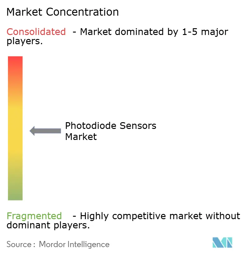
Market concentration remains moderate. Hamamatsu Photonics booked FY2024 net sales of JPY 203,961 million (USD 1.37 billion) and is building a new Compound Semiconductor Fab Center to lift opto-semiconductor output. Coherent Corp.’s diversified optics portfolio delivered USD 1.43 billion revenue in Q2 FY25, notching 27% growth through balanced participation in communications, instrumentation, and electronics. SICK AG and Endress+Hauser joined forces in a 50-50 joint venture to embed sensor suites into process-automation channels, broadening cross-selling capacity in refinery and chemical plants.
Strategic playbooks center on vertical integration and differentiated IP. Sony advances stacked SPAD designs to lock in automotive Tier-1s, while onsemi scales indirect time-of-flight sensors for industrial automation, giving OEMs a single-vendor route from pixel to software. TDK’s Spin Photo Detector showcases an emerging niche where spintronics can multiply data-throughput by 10×, aiming to secure sockets in AI inference clusters. Up-starts such as Lidwave leverage 4D lidar-on-chip integration, compressing cost and bill-of-materials, which threatens incumbent price umbrellas.
Supply-chain de-risking remains top of mind. Players pursue dual-sourcing for indium and gallium and evaluate chalcogenide alternatives to germanium, aligning with ESG mandates and reducing trade-policy exposure. Organic and perovskite photodiodes present low-temperature, solution-processed substitutes that may disrupt incumbent wafer-based economics in low-cost consumer and IoT nodes.
Photodiode Sensors Industry Leaders
-
Hamamatsu Photonics K.K
-
Thorlabs, Inc.
-
Edmund Scientific Corporation (Edmund Optics)
-
Centronic, Ltd.
-
Excelitas Technologies Corporation
- *Disclaimer: Major Players sorted in no particular order
Photodiode Sensors Market Companies Covered in this Report
- Hamamatsu Photonics K.K.
- Thorlabs Inc.
- Edmund Scientific Corporation (Edmund Optics)
- Centronic Ltd.
- Excelitas Technologies Corp.
- Vishay Intertechnology Inc.
- ams-Osram AG
- First Sensor AG (TE Connectivity)
- Everlight Electronics Co.
- Kyoto Semiconductor Co. Ltd.
- onsemi
- TT Electronics plc
- OSI Optoelectronics
- Nisshinbo Micro Devices
- Broadcom Inc.
- Renesas Electronics Corp.
- Rohm Semiconductor
- Sony Semiconductor Solutions
- Teledyne e2v
Market Opportunities and Future Outlook
A key whitespace is deeper integration of photodiodes into qualified sub-assemblies and platforms where compliance, calibration, and documentation come bundled with the hardware. Buyers in aerospace, defense, medical, and industrial automation often prioritize traceability and repeatability over lowest unit cost, which creates room for suppliers that pair photodiodes with metrology-grade calibration and controlled build processes, as reflected in Thorlabs NIST/PTB-traceable calibration practices for photodiode power sensors. Suppliers that operate within ISO 9001:2015, ISO 14001, and ISO 13485 frameworks (cited by Edmund Optics) can also better support regulated customer programs that require consistent documentation, change control, and validated test.
Another opportunity is supply-chain de-risking for indium/gallium-linked detector technologies and reducing customer time-to-market through broader component ecosystems. Hamamatsu Photonics points to responsible-minerals due diligence using RMI CMRT/EMRT templates aligned with OECD guidance, which maps to OEM pressure for auditable sourcing and may favor suppliers with established compliance infrastructure. On the productization side, vendors expanding ready-to-integrate photonics building blocks, including easier-to-source optical subcomponents and qualified assemblies, can shorten sensor-module design cycles in telecom, LiDAR/ADAS, and medical imaging programs where discrete-component integration time is a recurring bottleneck.
Recent Industry Developments in Photodiode Sensors Market
- June 2026: Hamamatsu Photonics K.K renaming of subsidiary NKT Photonics A/S to Hamamatsu Photonics A/S, integrating as Lasers and Fibers Business Unit following 2024 acquisition. The consolidation of photonics capabilities strengthens the supplier base for high performance laser and fiber components and supports cross selling across adjacent markets. Brand integration and unified operations across laser and fiber offerings improve efficiency and market reach across photonics applications.
- April 2026: Thorlabs Inc groundbreaks for a 70,000 sq ft expansion of its manufacturing facility in Ely, United Kingdom. The expansion increases photonics manufacturing capacity and supports scaling of optics components. The project improves local supply chain resilience and enables greater production throughput for end users in high growth sensor and imaging markets.
- April 2026: Edmund Optics releases off the shelf Extended Depth of Focus EDOF metalenses for laser systems. The introduction of simplified optical components for laser systems supports integration into photonics assemblies. The development can shorten time-to-market for sensor modules by enabling more compact and versatile optical designs.
Photodiode Sensors Market Report Scope and Research Methodology
Market Definition and Coverage
For this report, the photodiode sensors market covers packaged and discrete photodiode sensing components used to convert light into electrical signals across industrial, medical, telecom, automotive, and consumer use cases, captured as revenue at the point of sale in USD.
Scope exclusions: We exclude full optical modules and finished equipment where the photodiode is only one sub-component (for example, complete camera systems or full medical devices).
Segments Covered in This Report
- By Sensor Type
- PN Photodiode
- PIN Photodiode
- Avalanche Photodiode (APD)
- Schottky Photodiode
- By Material
- Silicon (Si)
- Silicon-Germanium (SiGe / Ge)
- Indium Gallium Arsenide (InGaAs)
- InGaAsP / InP
- Gallium Nitride (GaN)
- By Spectral Range
- Ultraviolet (200-400 nm)
- Visible (400-700 nm)
- Near-Infrared (0.7-1.4 µm)
- Short-Wave IR (1.4-3 µm)
- Mid/LW IR (>3 µm)
- By End-user Industry
- Consumer Electronics
- Telecommunications
- Aerospace and Defense
- Healthcare
- Automotive
- Industrial Automation and IoT
- Security and Surveillance
- By Geography
- North America
- United States
- Canada
- Mexico
- South America
- Brazil
- Argentina
- Rest of South America
- Europe
- Germany
- United Kingdom
- France
- Italy
- Russia
- Rest of Europe
- APAC
- China
- Japan
- South Korea
- India
- ASEAN
- Rest of APAC
- Middle East and Africa
- GCC
- Turkey
- South Africa
- North America
Data Sources, Market Sizing, and Validation
Desk Research
Desk work started by mapping where photodiodes are produced, shipped, and adopted, then aligning it with how demand shows up in end markets. Public sources such as US Census trade statistics, UN Comtrade, the International Telecommunication Union, and OECD industrial indicators were used to set direction on electronics output and cross-border movement for relevant component categories.
To ground the technical and application side, we also reviewed open materials such as IEEE and SPIE publications, standards notes from bodies like IEC, and select patent databases to see what device structures and wavelength bands are being pushed into volume products. These were complemented by company filings, earnings decks, association pages, and reputable press coverage for capacity additions, pricing commentary, and end-use demand signals. The sources listed here are illustrative and not exhaustive, since additional references were used for data collection, cross-checks, and clarification.
Primary Interviews and Surveys
Primary work was used to validate where revenue is actually booked and how demand is split by use case, which is not always clear from public sources. We spoke with participants across the value chain, including component suppliers, channel partners, and OEM and integrator-side stakeholders. Coverage was balanced across major manufacturing and consumption regions so assumptions could be tested in more than one market context.
Distribution of primary research fieldwork respondents
| Company type | Respondent position | Region |
|---|---|---|
| Top tier: 34% | CXOs: 16% | APAC: 49% |
| Mid tier: 48% | Functional/Unit leaders: 34% | EMEA: 33% |
| Smaller Players: 18% | Managers: 50% | Americas: 18% |
Market-Sizing & Forecasting
Sizing was built using a top-down approach where electronics and photonics demand pools were reconstructed through end-use adoption, with country-level rollups subsequently aligned to global totals. The model was then corroborated through selective bottom-up checks, including sampled supplier revenue signals, channel feedback on unit volumes, and ASP-by-application sanity checks, which helped adjust for mix changes without forcing a fully bottom-up build.
Key inputs that influenced the totals included telecom and datacom build activity, the pace of industrial automation and safety sensing adoption, medical sensing volumes in common optical measurement use cases, automotive sensing content per vehicle, and typical ASP spreads by material and spectral range. Since pricing can shift with integration and packaging choices, ASP progression was handled as an input that changes by application rather than as a single flat inflation uplift.
For forecasting, scenario analysis was used around a central case so the outlook stayed explainable and tied to observable indicators from interviews and public series. Where bottom-up signals were incomplete in smaller countries or niche applications, gaps were handled through proxy ratios based on comparable markets and then rechecked with primary feedback before finalization.
Data Validation & Update Cycle
Outputs were checked through triangulation across independent signals, and variance flags were reviewed before the model was signed off. When a country result looked out of line, inputs were rechecked, assumptions were traced back to sources, and follow-up calls were triggered to confirm whether the issue was scope, timing, or pricing.
Each report is refreshed annually, and interim updates are made when material events occur such as demand shocks, major capacity changes, or policy shifts that affect trade and supply. Before delivery, a final analyst pass is completed so clients receive an updated view aligned to the latest available data.
Mordor Intelligence's Photodiode Sensors Market Size Compared Against Other Published Estimates
Published market numbers for photodiode sensors can look far apart because the scope boundary is not always the same, and the pricing logic can be handled differently across applications. Differences also come from base-year selection, whether values are reported at component level or module level, and how quickly assumptions are refreshed when end markets move.
By tracking application-level unit demand and refreshing the ASP mix by material and wavelength band, Mordor Intelligence keeps the total tied to discrete photodiode component revenues, instead of mixing in broader optical modules or system-level spending.
Benchmark comparison
| Source | Market Size | Gaps in Research Methodology |
|---|---|---|
| Mordor Intelligence | USD 0.83 B (2026) | |
| Global Research Platform A | USD 0.87 B (2025) | Uses a different base year and appears to blend photodiode types and materials into a single ASP curve, which can overstate value when lower-cost silicon devices dominate volume. |
| Press Release Digest B | USD 1.00 B (2022) | Anchors the series to an earlier year and is likely broader on scope, so some module or system-adjacent revenue can be captured alongside discrete sensor components. |
The table shows that the spread is mainly explained by timing and what is counted as a photodiode sensor sale, rather than a disagreement on the direction of demand. When scope is kept at the discrete component level and prices are updated by application mix, the estimate becomes easier to audit and repeat with clear inputs.
Key Questions Answered in the Report
What is the current value of the photodiode sensors market?
The photodiode sensors market is valued at USD 825.82 million in 2026 and is projected to reach USD 1,164.64 million by 2031.
Which region leads the photodiode sensors market?
Asia-Pacific holds 45.55% revenue share owing to concentrated semiconductor manufacturing and aggressive 5G deployments.
Which segment grows fastest within the photodiode sensors market?
Automotive LiDAR applications show the highest CAGR at 8.62% during 2026-2031.
What material dominates photodiode production today?
Silicon remains dominant with 57.38% market share, though silicon-germanium and InGaAs are gaining ground for infrared performance.
How are supply chain risks affecting photodiode availability?
Export restrictions on gallium and indium create pricing and lead-time volatility, pushing manufacturers to explore alternative materials.
What is the forecast CAGR for the overall photodiode sensors market?
The market is expected to grow at a 7.12% CAGR between 2026 and 2031.