Market Size of Panel Level Packaging Industry

| Study Period | 2019-2029 |
| Market Size (2024) | USD 0.25 Billion |
| Market Size (2029) | USD 1.38 Billion |
| CAGR (2024 - 2029) | 41.07 % |
| Fastest Growing Market | Asia Pacific |
| Largest Market | Asia Pacific |
| Market Concentration | Medium |
Major Players
*Disclaimer: Major Players sorted in no particular order |
Panel Level Packaging Market Analysis
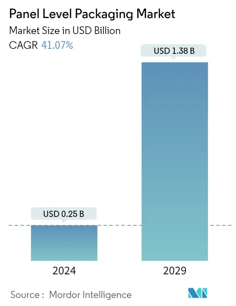
The Panel Level Packaging Market size is estimated at USD 0.25 billion in 2024, and is expected to reach USD 1.38 billion by 2029, growing at a CAGR of 41.07% during the forecast period (2024-2029).
The semiconductor industry is witnessing rapid growth, with semiconductors emerging as the basic building blocks of all modern technology. The advancements and innovations in this field directly impact all downstream technologies and drive the need for the market studied.
- With the importance of the semiconductor industry growing, the demand for enhanced packaging solutions is also increasing, leading to the development of new semiconductor packaging techniques.
- Panel-level packaging (PLP) is a technology that has gained prominence recently. PLP refers to semiconductor packaging processed on a panel size. In panel-level packaging, the assembly process includes the fabrication of die attach, redistribution lines, molding, and bumping at the panel level.
- As more packages may be processed in panel and parallel formats, this type of packaging facilitates a much better area utilization (ratio between panel/wafer size and package size) compared to round wafer shapes. Hence, a lower packaging cost is among the primary drivers for the market's growth. PLP has a lower environmental impact due to a lower waste generation and carbon footprint.
- The panel-level packaging (PLP) market also encounters certain challenges. The substantial expenses linked to the technology and the intricate nature of its implementation might impede its extensive acceptance. The packaging process involves both types, mold first and RDL first. However, the type of packaging involves problems in die shift. Shifting the die is considered one of the biggest issues as it may cause lesser yield or negatively influence the yields. This increases the need for more control over the packaging process and adds complexity, restraining the market's growth.
- In the post-COVID-19 period, the focus on panel-level packaging is anticipated to increase due to the cost benefits and the expansion of the packaging size from wafers to larger panel formats. Increasing the number of packages manufactured in parallel is another major advantage supporting the market's growth. PLP may adopt processes, materials, and equipment from other technology areas. Printed circuit boards (PCB), liquid crystal displays (LCD), or solar equipment are manufactured on panel sizes and offer new approaches for fan-out panel-level packaging.
Panel Level Packaging Industry Segmentation
Panel-level packaging is one of the following steps for fan-out wafer-level packaging. Vendors worldwide are focusing on upscaling PLP instead of drawing a roadmap to 450 mm fan-out wafer-level packaging. PLP is expected to offer significant cost advantages by parallelizing process steps and allowing higher area utilization of packages in rectangular panel formats rather than round wafer shapes to lower material waste.
The panel level packaging market is segmented by industry application (consumer electronics, automotive, telecommunication, and other industry applications) and geography (United States, China, Korea, Taiwan, Japan, Europe, Rest of the World). The report offers the market size in value terms in USD for all the abovementioned segments.
| By Industry Application | |
| Consumer Electronics | |
| Automotive | |
| Telecommunication | |
| Other Industry Applications |
| By Geography | |
| United States | |
| China | |
| Korea | |
| Taiwan | |
| Japan | |
| Europe | |
| Rest of the World |
Panel Level Packaging Market Size Summary
The panel-level packaging (PLP) market is experiencing significant growth, driven by the rapid expansion of the semiconductor industry, which is becoming increasingly integral to modern technology. PLP technology, which involves semiconductor packaging at the panel level, offers advantages such as better area utilization and reduced packaging costs compared to traditional round wafer shapes. This technology is particularly beneficial for consumer electronics, where the demand for miniaturization and efficient space utilization is high. The market is also supported by the growing adoption of 5G and IoT technologies, which create demand for more advanced and compact semiconductor solutions. Despite its advantages, the PLP market faces challenges, including high implementation costs and complexities in the packaging process, which could hinder its widespread adoption.
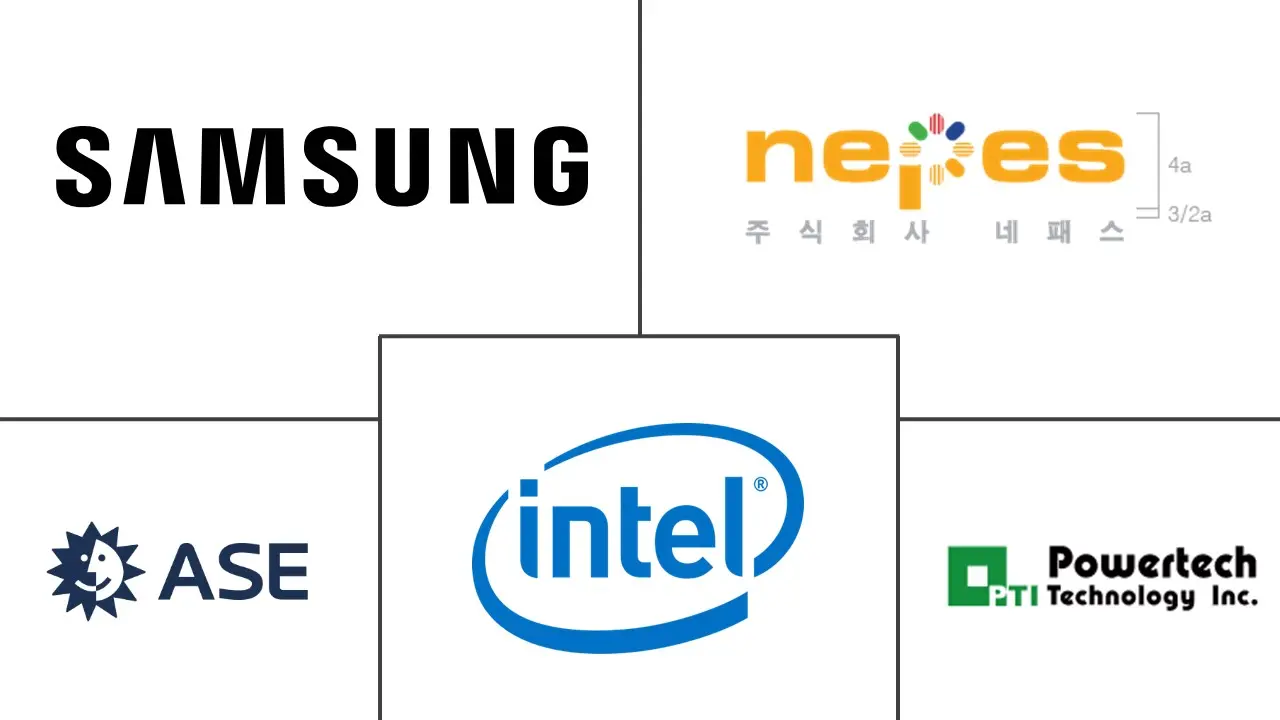
China plays a pivotal role in the panel-level packaging market due to its status as a leading consumer and producer of electronics, as well as its rapid 5G adoption. The country's electronics manufacturing sector continues to expand, supported by initiatives to boost growth and infrastructure development for 5G. The increasing demand for 5G-enabled devices and advancements in automotive technology further bolster the market. The panel-level packaging market is semi-consolidated, with major players like Samsung Electronics, Intel Corporation, and ASE Group actively engaging in partnerships and acquisitions to enhance their offerings. Recent developments, such as NEPES's intelligent semiconductor for edge computing and USI's factory expansion in Poland, highlight the ongoing innovation and strategic moves within the industry to maintain competitive advantage and meet growing market demands.
Panel Level Packaging Market Size - Table of Contents
-
1. MARKET INSIGHTS
-
1.1 Market Overview
-
1.2 Industry Attractiveness - Porter's Five Forces Analysis
-
1.2.1 Bargaining Power of Suppliers
-
1.2.2 Bargaining Power of Buyers
-
1.2.3 Threat of New Entrants
-
1.2.4 Threat of Substitute Products
-
1.2.5 Intensity of Competitive Rivalry
-
-
1.3 Industry Value Chain/Supply Chain Analysis
-
1.4 Assessment of Impact of Macroeconomic Factors on the Market
-
-
2. MARKET SEGMENTATION
-
2.1 By Industry Application
-
2.1.1 Consumer Electronics
-
2.1.2 Automotive
-
2.1.3 Telecommunication
-
2.1.4 Other Industry Applications
-
-
2.2 By Geography
-
2.2.1 United States
-
2.2.2 China
-
2.2.3 Korea
-
2.2.4 Taiwan
-
2.2.5 Japan
-
2.2.6 Europe
-
2.2.7 Rest of the World
-
-
Panel Level Packaging Market Size FAQs
How big is the Panel Level Packaging Market?
The Panel Level Packaging Market size is expected to reach USD 0.25 billion in 2024 and grow at a CAGR of 41.07% to reach USD 1.38 billion by 2029.
What is the current Panel Level Packaging Market size?
In 2024, the Panel Level Packaging Market size is expected to reach USD 0.25 billion.

