
Mobile Phone Semiconductor Market Size and Share
Market Overview
| Study Period | 2020 - 2031 |
|---|---|
| Market Size (2026) | USD 41.82 Billion |
| Market Size (2031) | USD 70.49 Billion |
| Growth Rate (2026 - 2031) | 11.03 % |
| Fastest Growing Market | Asia Pacific |
| Largest Market | Asia Pacific |
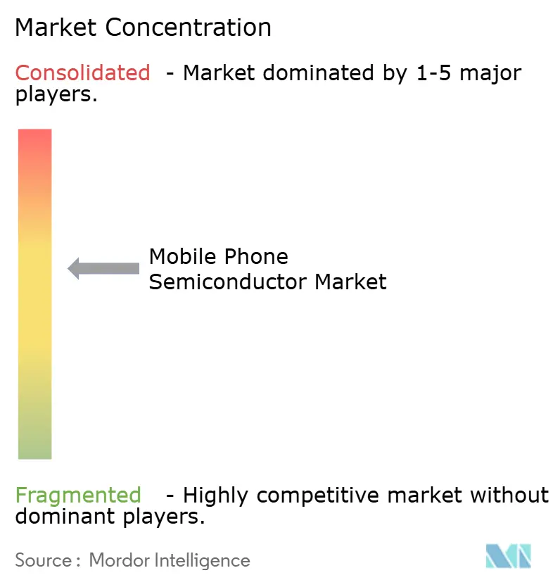
| Market Concentration | Medium |
Major Players
*Disclaimer: Major Players sorted in no particular order Image © Mordor Intelligence. Reuse requires attribution under CC BY 4.0. |
|
Mobile Phone Semiconductor Market Analysis by Mordor Intelligence
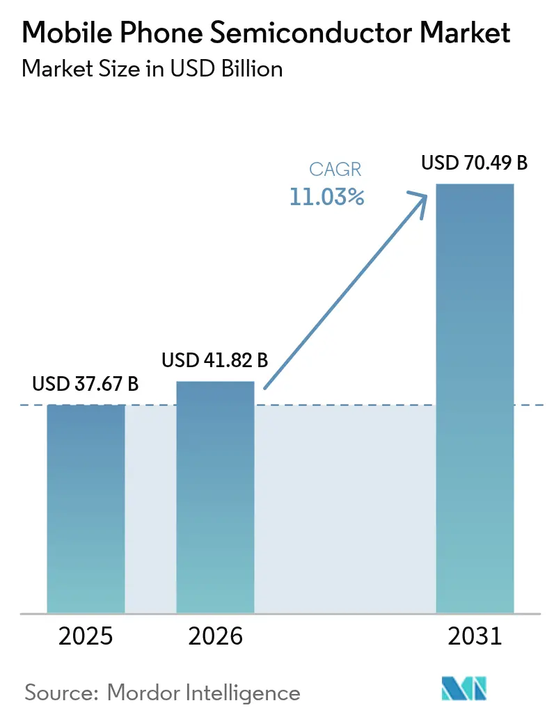
The mobile phone semiconductor market size in 2026 is estimated at USD 41.82 billion, growing from 2025 value of USD 37.67 billion with 2031 projections showing USD 70.49 billion, growing at 11.03% CAGR over 2026-2031. The rapid adoption of AI-native system-on-chip (SoC) designs, tighter integration of 5G radios, and escalating demand for specialized sub-3nm silicon form the backbone of this expansion. Foundry progress at 2 nm has enabled smartphone brands to embed neural processing units that deliver 45 TOPS of on-device inference without jeopardizing battery life. Memory density continues its upward trajectory as handset DRAM moves from 8 GB to 12 GB, while UFS 4.0 storage eases AI model loading constraints.[1] The race to standardize satellite connectivity and Wi-Fi 7 further broadens silicon content per device, fueling the adoption of multi-chip packages in advanced packaging lines across the Asia-Pacific region.
Key Report Takeaways
- By component, mobile processors captured 32.80% of the mobile phone semiconductor market share in 2025, while sensors are projected to expand at a 12.60% CAGR through 2031.
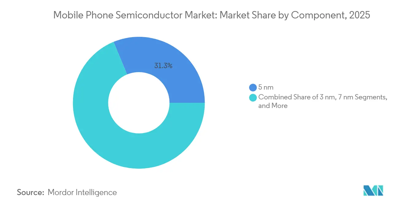
- By technology node, 5 nm devices accounted for 31.25% of the mobile phone semiconductor market size in 2025; sub-3 nm nodes are projected to achieve a 12.45% CAGR through 2031.
- By geography, the Asia-Pacific region held 53.90% of the mobile phone semiconductor market in 2025 and is expected to post a 12.05% CAGR through 2031.
- TSMC’s USD 42 billion capital spending plan, covering eight new fabs, highlights the investment intensity driving the mobile phone semiconductor market.
Note: Market size and forecast figures in this report are generated using Mordor Intelligence’s proprietary estimation framework, updated with the latest available data and insights as of 2026.
Market Trends and Insights
Drivers Impact Analysis of Mobile Phone Semiconductor Market*
| Driver | (~) % Impact on CAGR Forecast | Geographic Relevance | Impact Timeline |
|---|---|---|---|
| Proliferation of 5G smartphones | +2.8% | Global, with APAC leading adoption | Medium term (2-4 years) |
| Rising adoption of on-device AI/ML | +3.2% | North America and EU early adopters, APAC volume growth | Long term (≥ 4 years) |
| Growing memory content per handset | +1.9% | Global, driven by flagship segment expansion | Medium term (2-4 years) |
| High-refresh OLED displays | +1.4% | APAC manufacturing, global consumption | Short term (≤ 2 years) |
| Satellite connectivity enablement | +0.9% | North America and EU regulatory approval, global rollout | Long term (≥ 4 years) |
| Fan-out wafer-level SiP adoption | +0.8% | APAC manufacturing hubs, global implementation | Medium term (2-4 years) |
| Source: Mordor Intelligence | |||
Proliferation of 5G Smartphones
Surging shipment volumes of 5G handsets continue to propel the mobile phone semiconductor market onto a high-growth trajectory. Qualcomm’s X85 modem delivers 10 Gbps peak throughput and incorporates AI-assisted signal processing, increasing RF front-end module dollar content by nearly 20% per unit.[2] The leap from 4G to 5G requires multi-band power amplifiers, sub-6 GHz and mmWave antennas, and tighter thermal management, each of which adds die area. Samsung’s Exynos Modem 5400 introduced satellite fallback in 2024, ensuring continuous connectivity in remote areas. These requirements amplify wafer starts at 7 nm for modems and at mature 28 nm for companion RF transceivers, underlining how a single handset SKU often pulls wafers from four distinct process nodes. Consequently, fab utilization at APAC foundries remains elevated, sustaining supply pressure that benefits the mobile phone semiconductor market.
Rising Adoption of On-Device AI/ML
AI inferencing is migrating on-device to reduce latency and maintain privacy, thereby increasing compute density targets for application processors. MediaTek’s MT6825 demonstrated 40% energy savings compared to cloud-based inference, highlighting the cost advantages associated with local processing. Neural engines must coexist with CPUs, GPUs, image signal processors, and 5G basebands on a single substrate, driving chiplet-based SoC designs. Apple’s latest A-series processor integrates AI accelerators that execute large language models locally, prompting Android vendors to pivot toward dedicated tensor units that deliver 45 TOPS. This functionality utilizes more SRAM and high-speed inter-chip interconnects, driving demand for advanced packaging that keeps logic and memory in proximity. The outcome is a wider silicon footprint per handset, reinforcing double-digit revenue expansion for the mobile phone semiconductor market.
Growing Memory Content Per Handset
Handsets now function as AI workstations, demanding ample memory to stage large data sets. Samsung’s LPDDR5 at 12.7 GT/s meets the 2024 flagship needs, yet the roadmap to LPDDR6 at 17 GT/s in 2026 positions memory makers for a step-up in pricing. UFS 4.0 has entered mass deployment, with UFS 5.0 development achieving sequential read speeds of over 4.2 GB/s. As the median DRAM stack shifts from 8 GB to 12 GB, the dollar value of every mobile phone semiconductor market bill of materials expands. Rising bandwidth presents board-level challenges related to power rail stability and heat dissipation, driving an increased demand for power management ICs and thermal interface materials. Foundries benefit because LPDDR6 relies on process shrinks below 10 nm, locking incremental capacity into premium geometries where margins remain strongest.
High-Refresh OLED Displays
Mainstream phones now feature 120 Hz panels; gaming models are edging toward 144 Hz. Variable refresh logic necessitates agile timing controllers fabricated at 28 nm, while Samsung Display’s 22 nm driver IC cuts power by 40%. MagnaChip’s adaptive driver raised everyday battery life 25%. As foldable form factors proliferate, each hinge-based segment demands distinct controllers and touch-sensing ASICs, effectively doubling driver silicon content. These trends enhance the total available market for specialized analog and mixed-signal IC suppliers, tightening competition yet broadening revenue pools across the mobile phone semiconductor market.
Restraints Impact Analysis of Mobile Phone Semiconductor Market*
| Restraint | (~) % Impact on CAGR Forecast | Geographic Relevance | Impact Timeline |
|---|---|---|---|
| Supply-chain cyclicality and pricing pressure | -1.8% | Global, with APAC manufacturing concentration | Short term (≤ 2 years) |
| Geopolitical export restrictions | -2.1% | US-China trade corridor, global supply chains | Long term (≥ 4 years) |
| Sub-5 nm thermal/yield challenges | -1.2% | Advanced foundries in Taiwan, Korea, US | Medium term (2-4 years) |
| OEM consolidation trimming TAM for tier-2 vendors | -0.7% | Global, concentrated in Android ecosystem | Medium term (2-4 years) |
| Source: Mordor Intelligence | |||
Supply-Chain Cyclicality and Pricing Pressure
Memory and analog cycles inject volatility into the mobile phone semiconductor market. Micron’s Q1 2025 revenue slipped 15% as DRAM prices softened, showing how a single quarter can erode margins across the value chain.[3] Seasonal handset ramps amplify boom-bust swings, leaving tier-2 suppliers exposed to inventory shocks. Capacity builds, often funded during peak demand, flood the market just as demand normalizes. The resultant oversupply compresses average selling prices, yet simultaneously sparks consolidation that nudges the market toward higher concentration ratios over time.
Geopolitical Export Restrictions
The January 2025 tightening by the U.S. Bureau of Industry and Security mandates licenses for advanced AI chips, fragmenting global supply webs. Chinese OEMs now dual-source between domestic 14 nm fabs and overseas 5 nm foundries, adding cost and complexity. Equipment embargoes slow yield-ramp for sub-10 nm lines inside China, widening performance gaps in premium tiers. Western brands, meanwhile, must validate separate hardware builds for sanctioned geographies, diverting limited engineering resources. These frictions temper the otherwise robust trajectory of the mobile phone semiconductor market.
*Our forecasts treat driver/restraint impacts as directional, not additive. The impact forecasts reflect baseline growth, mix effects, and variable interactions.
Mobile Phone Semiconductor Market Segment Analysis
By Component:
Processors Drive Integration TrendsMobile processors retained a 32.80% market share of the mobile phone semiconductor market in 2025, underscoring their status as architectural hubs that coordinate AI inference, 5G connectivity, imaging pipelines, and sensor fusion within an increasingly compact board footprint. The mobile phone semiconductor market size associated with this component class is forecast to grow at an 10.88% CAGR through 2031, as chiplets and advanced packaging drive another wave of integration density. Sensors, the fastest-growing component group with a 12.60% CAGR, meet the rising demand for multimodal biometric authentication, air-quality tracking, and contextual awareness required by AI assistants.
Memory ICs anchor AI-native workloads through higher-bandwidth DRAM, while Logic ICs evolve into domain-specific accelerators that offload narrow AI kernels. Analog ICs still matter for signal conditioning even as digital take-over accelerates. Power management IC complexity increases with multi-standard fast charging and dynamic voltage scaling tailored to AI engines. RF and connectivity ICs now integrate Wi-Fi 7, Bluetooth 5.4, and soon satellite transceivers, swelling per-handset BOM. Display driver ICs incorporate variable refresh intelligence, and Audio ICs feature spatial playback and on-chip noise cancellation DSPs that align with trends in videogames and immersive media.

By Technology Node:
Sub-3 nm Emergence Reshapes EconomicsThe 5 nm class accounted for 31.25% of the mobile phone semiconductor market size in 2025, striking a balance between performance and cost for flagship volumes. Yet sub-3 nm wafers are expanding at a 12.45% CAGR as TSMC’s N2 node enters mass production for Apple’s next-generation SoCs. The mobile phone semiconductor market now features a barbell cost curve: cutting-edge 2nm logic fetches premium margins, while mature 28nm lines churn out power-management and RF chips at scale.
7 nm remains the workhorse for mid-premium devices, whereas 16 nm and 28 nm processes anchor connectivity and analog functions where leakage trumps outright speed. Nodes above 28 nm persist for resilience-critical RF front ends. Samsung’s gate-all-around transistors at 3 nm promise a 35% power reduction but still struggle with yield issues. Intel’s foundry services entice U.S. brands seeking geographic diversification, though wafer pricing challenges the Asian incumbency. The economic backdrop illustrates why the mobile phone semiconductor market remains a tale of two cost structures rather than a monolithic curve.
Geography Analysis
APAC Mobile Phone Semiconductor Market
The Asia-Pacific region held 53.90% of the mobile phone semiconductor market in 2025, driven by its deeply entrenched manufacturing clusters, government incentives, and proximity to handset assembly centers. China increased its installed wafer capacity by 13% to 8.6 million wafers per month in 2024, primarily at 28 nm nodes that supply power-management and connectivity devices. Taiwan dominates high-performance logic via TSMC, while Korea leads memory through Samsung and SK Hynix. India’s ascent as a large-scale assembly hub is creating adjacent demand for local test and packaging, stamping the region with a forecast 12.05% CAGR that exceeds the global baseline.
North America Mobile Phone Semiconductor Market
North America’s mobile phone semiconductor footprint hinges on design IP leadership and new fab investments catalyzed by the CHIPS Act. TSMC’s Arizona plant began 4 nm production in early 2025, offering capacity to premium U.S. handset brands. Intel’s USD 20 billion Ohio expansion envisions mobile-optimized capacity, although cost headwinds remain relatively higher compared to its Asian peers. The region benefits from tighter IP control and shorter R&D loops between design centers and advanced manufacturing lines.
EMEA and South America Mobile Phone Semiconductor Market
Europe prioritizes strategic autonomy and environmental sustainability. The EU Chips Act aims for a 20% global market share by 2030, allocating more funds toward automotive and industrial chips than handsets. GlobalFoundries–UMC merger talks aim to consolidate 10% of othe worldwide contract capacity, providing a brand with geopolitical balance. The Middle East and Africa offer prospects for back-end assembly as mobile phone vendors diversify. South America remains a modest participant, capped at final assembly, yet improving trade pacts could eventually draw test and package operations.

Regulatory Landscape
Trade and technology controls increasingly shape mobile phone semiconductor sourcing and compliance. In January 2026, the U.S. Bureau of Industry and Security (BIS) revised its license review policy for exports of specified advanced computing semiconductors to China and Macau, adding diligence needs across global design-to-manufacturing programs that share tooling, IP, or wafer capacity with restricted end markets.
On the trade side, the United States issued Proclamation 11002 under Section 232, imposing a 25% ad valorem duty on specified imported semiconductors and derivative products effective January 15, 2026, with exclusions that include non-data center consumer applications. Separately, the Office of the United States Trade Representative finalized a December 2025 Section 301 tariff action on Chinese semiconductors (0% at implementation, with a scheduled increase on June 23, 2027). In Europe, the European Commission advanced a 2026 proposal often referred to as the Chips Act 2.0 to reinforce EU capabilities across design, production, packaging, and recycling, supporting the broader policy push toward a more localized semiconductor value chain.
Value Chain Analysis
The value chain runs from EDA and IP (primarily ARM-based CPU/GPU ecosystems and EDA toolchains) through fabless design houses, including Qualcomm, MediaTek, and Apple, to foundry manufacturing, OSAT and advanced packaging, and handset OEM integration. At the leading edge, advanced node production is highly concentrated, with TSMC reported at 70.2% share of the global foundry market in Q2 2025. Access to 5 nm, 3 nm, and emerging 2 nm capacity therefore acts as a gating factor for premium mobile processors and tightly integrated modem-RF designs.
Downstream, OSAT and substrate availability increasingly influence smartphone silicon readiness as multi-chip packaging, SiP, and fan-out approaches expand content per device, including RF modules, power management, and high-bandwidth memory adjacency. Structural bottlenecks remain lithography and other critical tool lead times extending beyond 24 months, along with periodic constraints in high-purity materials. These constraints intensify allocation-driven behavior across nodes, as flagship SoCs compete for sub-5 nm wafer starts while RF, PMIC, and display drivers still depend on mature nodes such as 28 nm, leaving single handset platforms reliant on multiple process generations.
Competitive Landscape
The mobile phone semiconductor market rivalry centers on integration depth, power efficiency, and AI feature density, rather than raw clock speed. Qualcomm remains the reference for premium Android processors but faces stiff price-performance competition from MediaTek’s Dimensity line. Apple’s vertical stack insulates its flagship share and reinforces exclusive access to TSMC’s leading nodes. Samsung juggles dual roles: internal chipset supply and merchant sales, creating strategic tensions when customers overlap with its handset division.
Platform-level selling is ascendant. Vendors are increasingly bundling processors, RF modules, power management, and reference software to reduce OEM design cycles. RF competition intensifies as satellite connectivity normalizes, handing white-space to niche players specializing in L-band and S-band front ends. Packaging advances, fan-out wafer-level, 2.5D interposers, and chip-on-wafer-on-substrate translate into new battlegrounds where ASE, Amkor, and Intel vie for design wins.
Foundry selection has become a strategic lever. TSMC’s first-mover edge at 2 nm gives early adopters a six-month performance window, but Samsung’s gate-all-around roadmap and Intel’s U.S. capacity threaten to dilute that lead by 2027. Patent cross-licensing with ARM remains foundational, as every flagship SoC taps ARM CPU cores in some form.[4] Consolidation pressures loom because a single process node now demands more than USD 1 billion in R&D, favoring deep-pocketed incumbents.
Mobile Phone Semiconductor Industry Leaders
-
Qualcomm Incorporated
-
MediaTek Inc.
-
Samsung Electronics Co., Ltd.
-
Apple Inc.
-
HiSilicon Technologies Co., Ltd.
- *Disclaimer: Major Players sorted in no particular order
Mobile Phone Semiconductor Market Companies Covered in this Report
- Qualcomm Incorporated
- MediaTek Inc.
- Samsung Electronics Co., Ltd.
- Apple Inc.
- HiSilicon Technologies Co., Ltd.
- UNISOC Technologies Co., Ltd.
- Intel Corporation (Foundry Services)
- Advanced Micro Devices, Inc.
- NVIDIA Corporation
- Texas Instruments Incorporated
- Analog Devices, Inc.
- Skyworks Solutions, Inc.
- Qorvo, Inc.
- Murata Manufacturing Co., Ltd.
- NXP Semiconductors N.V.
- STMicroelectronics N.V.
- Infineon Technologies AG
- Micron Technology, Inc.
- SK hynix Inc.
- Kioxia Corporation
- Sony Semiconductor Solutions Corporation
- ON Semiconductor Corporation
- Dialog Semiconductor GmbH
- Cirrus Logic, Inc.
- Rohm Co., Ltd.
Market Opportunities and Future Outlook
A key opportunity is expanding geographically diversified manufacturing and packaging ecosystems to reduce concentration risk and increase local integration options for mobile silicon programs. In July 2026, the Government of India approved a second phase of the India Semiconductor Mission (ISM 2.0) with an outlay of Rs 1,27,500 crore and the Mobile Phone Manufacturing Scheme (MPMS) with an outlay of Rs 62,500 crore, both structured for five years starting FY 2026-27. This combination supports handset production scale-up alongside adjacent semiconductor and packaging activity, expanding whitespace for assembly, test, packaging, and locally optimized component supply for mid-range volumes.
A second whitespace area is advanced packaging and substrate capacity aligned to RF-SiP and high-density compute modules required by AI-centric smartphones. In June 2026, LG Innotek initiated plans for a new semiconductor substrate plant in Haiphong, Vietnam, targeting RF-SiP, FC-CSP, and FC-BGA substrates, signaling capacity positioning closer to Asia-Pacific electronics manufacturing clusters. On the product side, mid and entry tier platform refreshes, including Qualcomm introducing Snapdragon 6 Gen 5 and Snapdragon 4 Gen 5 (May 2026), create openings for OEMs to differentiate through on-device AI features, connectivity integration, and power efficiency without relying solely on flagship-class silicon.
Recent Industry Developments in Mobile Phone Semiconductor Market
- July 2026: Motorola launched the Edge 70 Max in India featuring the Qualcomm Snapdragon 8 Gen 5 chipset. The launch shows how flagship-tier platforms are used to anchor performance and AI feature positioning, supporting demand for leading-edge application processors and associated power management and RF content across premium device stacks.
- August 2025: TSMC outlined a USD 42 billion capital spending plan spanning eight new fabs and one advanced packaging site. The program underscores how capacity additions at advanced nodes and packaging are central to meeting smartphone SoC and AI-centric silicon requirements, and how it can shape allocation leverage for major mobile chip designers.
- July 2024: Samsung introduced the Exynos Modem 5400 with satellite connectivity fallback capability. The update expands silicon content per handset by adding satellite-ready modem and RF requirements, supporting incremental demand for RF front-end modules and multi-band connectivity components in compatible smartphone designs.
Mobile Phone Semiconductor Market Report Scope and Research Methodology
Market Definition and Coverage
This market covers the revenue value of semiconductor components designed into mobile phones, including processors and modem-related chips, memory, power and analog devices, RF and connectivity ICs, display drivers, audio ICs, and key sensors used in the handset.
Scope exclusions: We exclude semiconductors sold mainly for tablets, PCs, telecom infrastructure, and general consumer electronics that are not designed into a mobile phone build.
Segments Covered in This Report
-
By Component
- Mobile Processors
- Memory ICs
- Logic ICs
- Analog ICs
- Power Management ICs
- RF ICs and Connectivity ICs
- Display Driver ICs
- Audio ICs
- Sensors (Motion sensors, Environmental Sensors, Positioning Sensors, Image Sensors, Biometric Sensors, etc.)
-
By Technology Node
- < 3 nm
- 3 nm
- 5 nm
- 7 nm
- 16 nm
- 28 nm
- > 28 nm
-
By Geography
-
North America
- United States
- Canada
- Mexico
-
South America
- Brazil
- Argentina
- Rest of South America
-
Europe
- Germany
- United Kingdom
- France
- Italy
- Spain
- Rest of Europe
-
Asia-Pacific
- China
- Japan
- South Korea
- India
- Singapore
- Australia
- Rest of Asia-Pacific
-
Middle East and Africa
-
Middle East
- Saudi Arabia
- United Arab Emirates
- Turkey
- Rest of Middle East
-
Africa
- South Africa
- Nigeria
- Egypt
- Rest of Africa
-
Middle East
-
North America
Data Sources, Market Sizing, and Validation
Desk Research
Desk work starts with building a clean view of mobile phone shipments, network generation transitions, and the semiconductor content per device. We lean on public sources such as ITU indicators for mobile connectivity, World Bank macro series, national customs and trade statistics where available, and standards bodies and spectrum regulators for 4G and 5G rollout signals.
We also review annual reports, earnings decks, and investor commentary from relevant chip and handset supply chain participants to understand mix shifts, node transitions, and pricing direction. For cross-checks, we use paid subscriptions for company financials and intelligence, patent databases, and shipment-level import and export databases where they help validate trade flows. These examples are not exhaustive, and many other public sources were used for collection, validation, and clarification.
Primary Interviews and Surveys
Expert discussions and structured surveys were used to confirm what is inside the market scope and how fast key chip blocks are scaling in value per phone. We tested inputs with people across chip design, packaging and test, manufacturing, channel distribution, and device OEM procurement, and we maintained coverage across APAC, EMEA, and the Americas so regional mix effects were not missed.
Distribution of primary research fieldwork respondents
| Company type | Respondent position | Region |
|---|---|---|
| Top tier: 38% | CXOs: 21% | APAC: 41% |
| Mid tier: 40% | Functional/Unit leaders: 31% | EMEA: 36% |
| Smaller Players: 22% | Managers: 48% | Americas: 23% |
Market-Sizing & Forecasting
Our sizing starts from a top-down build where mobile phone unit shipments and the mix of smartphone tiers are translated into a dollar demand pool using typical semiconductor content per handset, then adjusted for 4G to 5G shifts and node migration. To keep totals grounded, the outputs are corroborated with selective bottom-up approximations such as sampled ASP times unit volumes for key chip groups and channel checks on mix changes, and then the totals are tuned when the two views do not align.
Model inputs include handset shipment volumes, 5G penetration and feature mix (such as modem RF complexity), average chip content value per phone, memory density trends, and the pace of advanced node adoption that influences ASP progression. When some chip categories have limited public signals in a country, we handle gaps by using region-level mix proxies, then rechecking against trade indicators and interview feedback.
For forecasting, scenario analysis is used around shipment growth and 5G and premium mix assumptions, and then the mid case is shaped using time series smoothing on historical device cycles. Assumptions on content growth per phone are only rolled forward when they are consistent with supplier commentary and expert views on bill of materials direction.
Data Validation & Update Cycle
Outputs are checked in multiple steps, starting with internal consistency tests across units, ASPs, and implied chip content per phone, followed by variance checks against independent shipment and macro indicators. If an outlier appears, the logic is revisited, and when needed, follow-up calls are done to confirm the assumption that is driving the swing.
Before sign-off, another analyst reviews the model math, the scope rules, and year-to-year movement so the story matches the numbers. The report is refreshed annually, with interim updates triggered by material events such as sharp shipment resets, major node transition delays, or sudden pricing moves. Right before delivery, a final pass is completed so clients receive the latest updated view.
Mordor Intelligence's Mobile Phone Semiconductor Market Growth Market Size Compared Against Other Published Estimates
Published numbers for mobile phone semiconductors often do not match because the included chip blocks, device coverage, and the year used for pricing conversion can differ. Differences also come from whether a study follows handset shipments and content per phone, or if it leans more on broad semiconductor revenue pools.
Some published estimates appear to use a wider device umbrella or add adjacent electronics beyond the handset. In Mordor Intelligence, the sizing is limited to semiconductors designed into mobile phones and is validated against handset shipment and 4G to 5G mix signals before the final totals are locked.
Benchmark comparison
| Source | Market Size | Gaps in Research Methodology |
|---|---|---|
| Mordor Intelligence | USD 41.82 B (2026) | |
| Industry Publisher A | USD 40.88 B (2025) | Uses a different base year and may apply broader supply chain language, which can shift what gets counted as mobile phone specific chips and how FX timing is handled in the conversion. |
| Industry Research Group B | USD 67.93 B (2025) | Appears to sit on a wider device and component scope, which can pull in semiconductor revenue not strictly tied to mobile phone builds and inflate the per device content assumption. |
The spread across sources is mainly explained by base year choice and how tightly the scope is tied to handset builds, rather than the direction of growth. By keeping the model linked to shipments, mix, and chip content signals, the final value stays traceable to a repeatable set of steps that can be revisited when market conditions change.
Key Questions Answered in the Report
What is the expected value of the smartphone semiconductor market in 2031?
It is projected to reach USD 70.49 billion by 2031, expanding at an 11.03% CAGR.
Which component currently leads revenue contribution?
Mobile processors held 32.80% market share in 2025, the highest among all component groups.
Why are sub-3 nm nodes important for future smartphone chips?
They enable higher AI TOPS performance and lower power consumption, supporting advanced use cases like on-device large language models.
How does Asia-Pacific dominate manufacturing?
The region combines large-scale wafer fabs, established packaging houses, and proximity to handset assembly lines, securing 53.90% market share in 2025.
What impact do export controls have on Chinese smartphone OEMs?
They restrict access to cutting-edge memory and AI chips, forcing reliance on domestically produced components that lag by one to two generations.
Which new connectivity feature is driving RF IC demand?
Satellite connectivity integration in mainstream handsets is creating additional demand for multi-band RF front-end modules.