
Micro LED Market Size and Share
Market Overview
| Study Period | 2020 - 2031 |
|---|---|
| Market Size (2026) | USD 0.56 Billion |
| Market Size (2031) | USD 2.17 Billion |
| Growth Rate (2026 - 2031) | 31.12 % |
| Fastest Growing Market | Middle East |
| Largest Market | Asia Pacific |
| Market Concentration | Medium |
Major Players *Disclaimer: Major Players sorted in no particular order Image © Mordor Intelligence. Reuse requires attribution under CC BY 4.0. | |
Micro LED Market Analysis by Mordor Intelligence
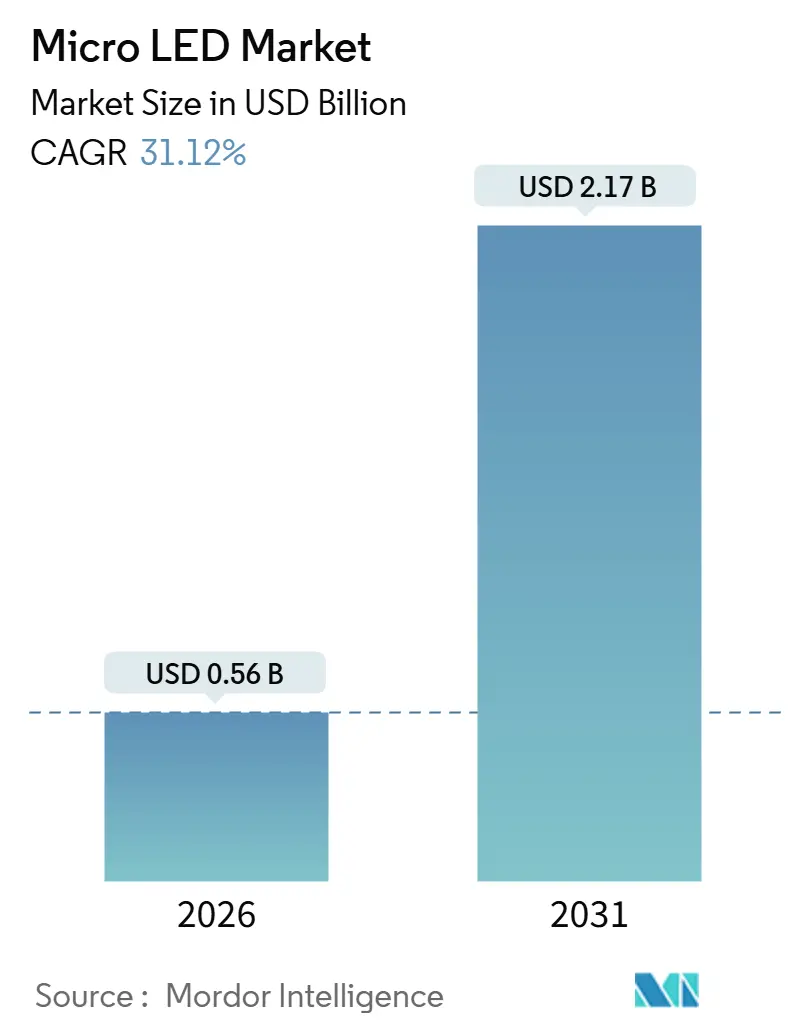
The Micro LED Market size is estimated at USD 0.56 billion in 2026, and is expected to reach USD 2.17 billion by 2031, at a CAGR of 31.12% during the forecast period (2026-2031). Surging capital re-allocation from OLED and mini-LED toward micro-scale epitaxy, together with defense procurement of ultra-bright head-up displays, underpins this expansion. Pilot lines in Taiwan, China, and South Korea are resolving the historic mass-transfer yield bottleneck, while quantum-dot color conversion trims epitaxial complexity and accelerates time-to-yield. Wearables remain the gateway use-case, yet near-eye augmented-reality devices, where 3,000+ PPI density is mandatory, are pacing the revenue curve. Fine-pitch digital signage is also scaling quickly as transparent modules replace static LED billboards in high-footfall retail corridors across Gulf Cooperation Council cities and East Asia. In parallel, healthcare theaters and robotic-surgery suites are adopting daylight-readable micro-LED monitors to reduce heat dissipation and improve color fidelity during minimally invasive procedures.
Key Report Takeaways
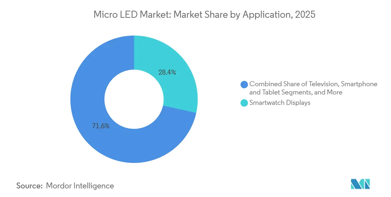
- By application, smartwatch displays led with 28.43% revenue share in 2025, near-to-eye devices (AR/VR) are forecast to expand at a 32.61% CAGR through 2031.
- By end-use industry, consumer electronics accounted for 40.12% of the Micro LED market share in 2025, while the healthcare sector is projected to grow at a 33.37% CAGR through 2031.
- By panel size, panels smaller than 10 inches accounted for a 46.78% share of the Micro LED market size in 2025; these panels are expected to advance at a 32.83% CAGR through 2031.
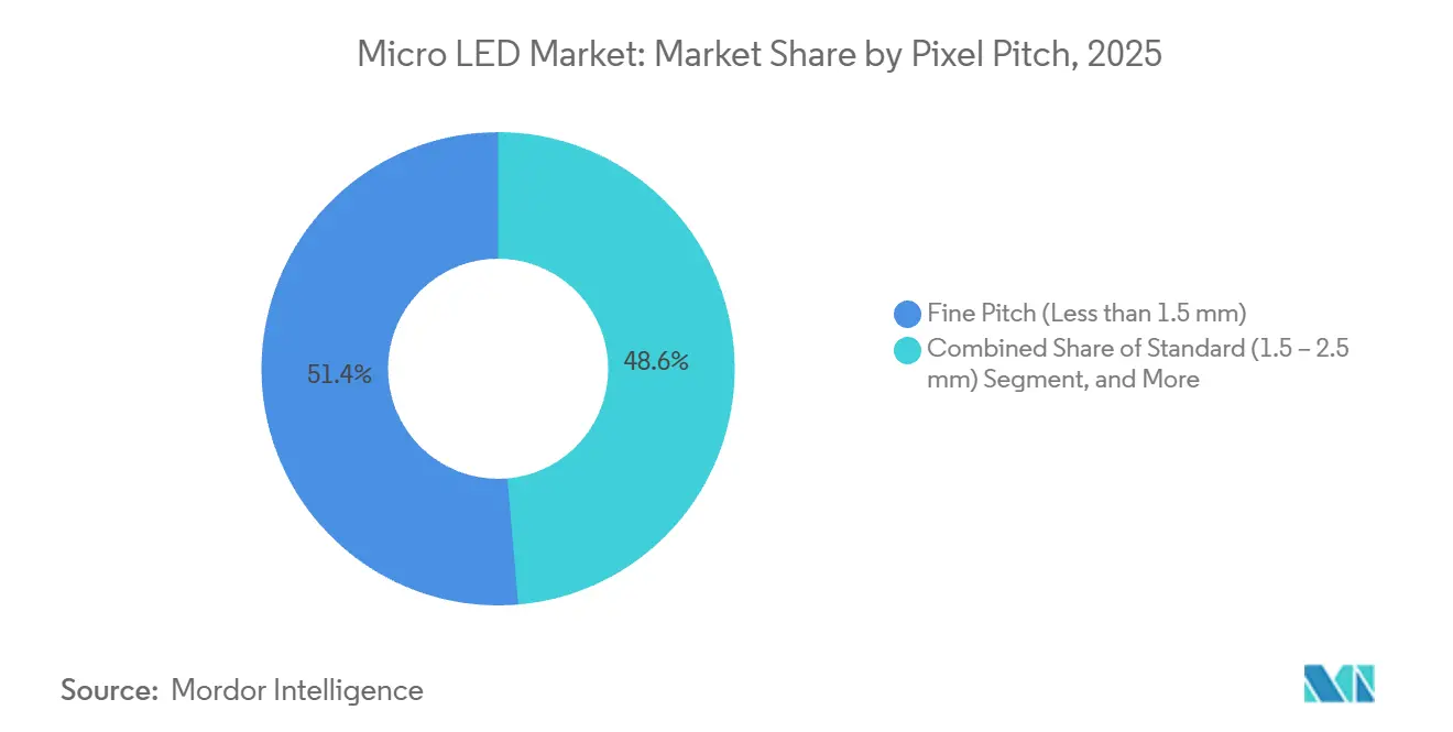
- By pixel pitch, fine-pitch panels with a pitch of under 1.5 mm commanded 51.36% of the revenue in 2025 and are expanding at a 33.46% CAGR.
- By technology, RGB full-color architectures accounted for 78.67% shipments in 2025 and are growing at a 35.79% CAGR.
- By component, epitaxial wafers accounted for a 34.28% revenue share in 2025; the Driver IC segment is expected to rise at a 34.23% CAGR through 2031.
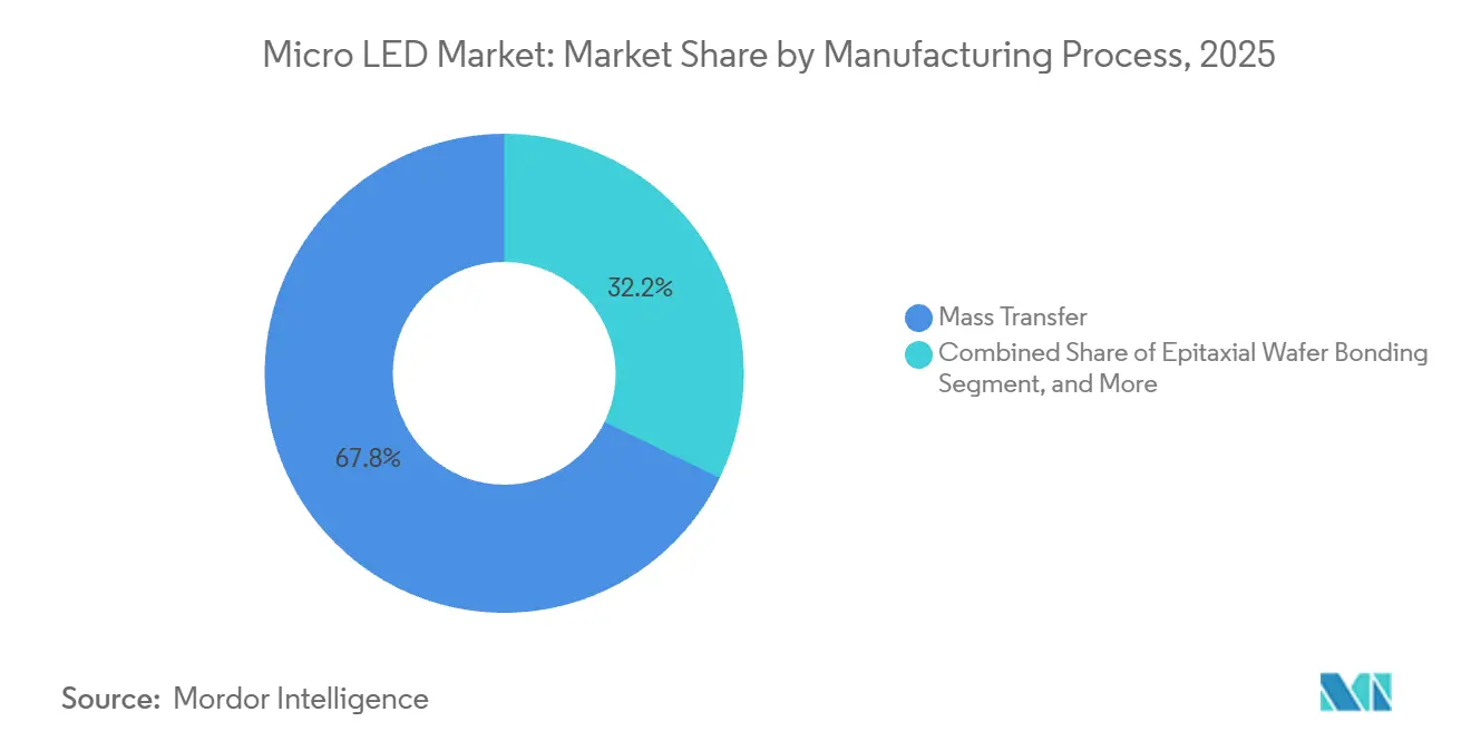
- By manufacturing process, mass transfer covered 67.81% of output in 2025; hybrid bonding is projected to climb at a 32.19% CAGR to 2031.
- By offering, display modules dominated with 71.24% revenue share in 2025; lighting modules are on track for a 32.04% CAGR through 2031.
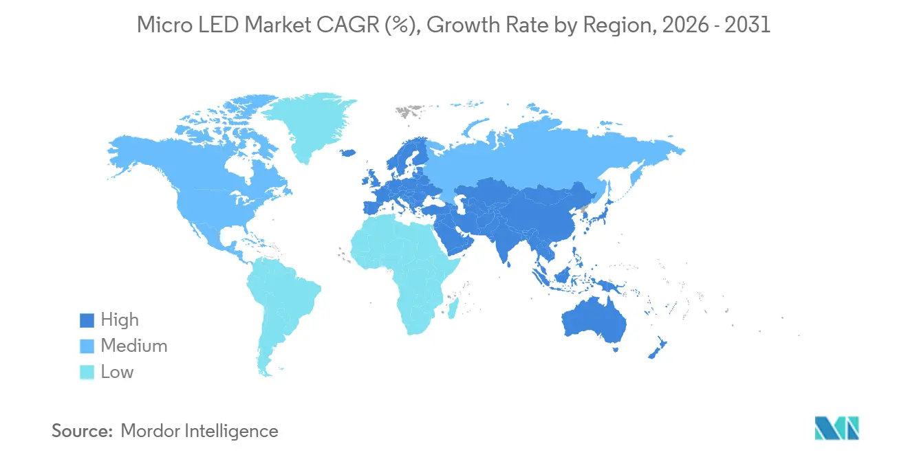
- By region, Asia Pacific led with 66.42% revenue share in 2025; Middle East is poised to expand at a 32.21% CAGR through 2031.
Note: Market size and forecast figures in this report are generated using Mordor Intelligence’s proprietary estimation framework, updated with the latest available data and insights as of January 2026.
Market Trends and Insights
Drivers Impact Analysis of Micro LED Market*
| Driver | (~) % Impact on CAGR Forecast | Geographic Relevance | Impact Timeline |
|---|---|---|---|
| Apple and Samsung Roadmaps for Micro-LED Wearables Accelerating Small-Display Demand | +6.2% | Global, Early Focus in North America and East Asia | Medium Term (2–4 Years) |
| Transparent and Flexible Retail Signage Uptake in Gulf Cooperation Council Countries and East Asia | +4.8% | Middle East and East Asia | Short Term (≤ 2 Years) |
| Defense-Grade Micro-Displays Funded by United States and EU Governments | +5.1% | North America and Europe | Medium Term (2–4 Years) |
| Taiwanese Mini-LED Cost Decline Enabling Pilot Micro-LED Lines | +7.3% | Global, Manufacturing in Taiwan | Long Term (≥ 4 Years) |
| European Automotive Sun-Readability Norms Boosting Micro-LED HUD Integration | +3.9% | Europe and Spillover Markets | Long Term (≥ 4 Years) |
| Quantum-Dot Color-Conversion Efficiency Breakthroughs Reducing Manufacturing Steps | +5.4% | Global | Medium Term (2–4 Years) |
| Source: Mordor Intelligence | |||
Apple and Samsung Roadmaps For Micro-LED Wearables Accelerating Small-Display Demand
Samsung’s CES 2025 concept smartwatch features a peak luminance of roughly 4,000 nits, quadrupling the luminance of today’s OLED wearables and confirming outdoor readability targets. Apple’s canceled watch project shifts micro-LED R&D toward near-eye AR glasses at its Santa Clara campus. Meta has locked in Plessey’s full GaN-on-Si capacity for late-2025 smart glasses, while JBD mass-produces monochrome and RGB panels for tier-one headset OEMs. Collectively, these roadmaps pivot demand from wrist-worn to sub-1-inch microdisplays requiring 3,000 PPI, a density OLED struggles to achieve at viable yield. Their trajectories signal that the micro LED market will diversify across multiple wearable form factors over the next four years.
Transparent and Flexible Retail Signage Uptake In Gulf Cooperation Council Countries and East Asia
Storefront and airport installations in Saudi Arabia, the United Arab Emirates, Tokyo, and Shanghai are deploying modules that deliver 70-85% transparency once pixels are off, maintaining sightlines while broadcasting video content. LG Display and BOE publicized prototypes under 5 mm thick that wrap around curved glass, addressing architectural mandates for glass façades in new smart-city districts. The region’s extreme ambient light-exceeding 100,000 lux-renders transparent OLED solutions unreadable outdoors, giving micro LED an intrinsic performance moat. Regulatory zoning that favors sightline preservation further accelerates uptake, making retail signage an early-scale driver of fine-pitch panels in the micro LED market.
Defense-Grade Micro-Displays Funded By United States and EU Governments
A U.S. Army contract awarded to Kopin in April 2025 defines full-color micro-LED requirements for head-mounted fire-control optics. DARPA’s LUMOS program finances heterogeneous integration of compound-semiconductor emitters with silicon photonics for compact optical systems. These initiatives seek 10,000+ nit daytime readability, −40 °C to +85 °C operation, and elimination of scan-line artifacts, benchmarks that OLED cannot reach. The resulting specifications flow down to commercial AR devices, anchoring a defense-to-consumer technology transfer that enlarges total addressable demand in the micro LED market.
Taiwanese Mini-LED Cost Decline Enabling Pilot Micro-LED Lines
Shared tooling from mature mini-LED fabs cuts incremental capex for micro-LED pilot lines. PlayNitride’s USD 19 million Kunshan site expands epitaxial capacity within mainland China and forecasts a consumer television cost inflection point by 2027. Ennostar divested Kfes Lighting to redeploy USD 30 million into a six-inch epi-wafer expansion, indicating a strategic exit from the commodity lighting market. AU Optronics plans the world’s largest dedicated micro-LED line for mass production in 2025, leveraging its thin-film-transistor expertise to integrate active-matrix backplanes. Collectively, Taiwanese moves reduce per-panel cost curves and unlock broader deployment of micro-scale dies, lifting the global micro LED market growth trajectory.
Restraints Impact Analysis of Micro LED Market*
| Restraint | (~) % Impact on CAGR Forecast | Geographic Relevance | Impact Timeline |
|---|---|---|---|
| Mass-Transfer Yield Below 60% for Sub-10 µm LEDs Beyond 4-Inch Wafers | −5.7% | Global, Acute in North America and Europe | Short Term (≤ 2 Years) |
| Non-Standardized Automotive Qualification Protocols | −2.9% | Global, Fragmentation in Asia Pacific and South America | Medium Term (2–4 Years) |
| GaN-on-Si Wafer Supply Concentration in Asia | −2.1% | Global Risk Centered in Taiwan, China, and Japan | Long Term (≥ 4 Years) |
| More Than USD 600 Million Capex Limiting Expansion in South America and Africa | −3.4% | South America and Africa | Long Term (≥ 4 Years) |
| Source: Mordor Intelligence | |||
Mass-Transfer Yield Below 60 % For Sub-10 µm LEDs Beyond 4-Inch Wafers
Nature’s September 2025 review confirms sidewall recombination and Auger effects erode yields once pixel pitch falls below 10 µm. Sub-5 µm LEDs demanded by AR microdisplays face catastrophic die loss during pick-and-place or laser lift-off transfer, limiting their commercial viability. PlayNitride’s March 2025 chip-on-carrier study improved yields but still documented industrial-scale gaps. High-PPI microdisplays in North America and Europe, therefore, remain expensive, slowing consumer adoption and subtracting momentum from the micro LED market until hybrid bonding or other wafer-level processes mature.
Non-Standardized Automotive Qualification Protocols
UNECE Regulations 112, 123, and 148 govern photometric limits but omit accelerated aging profiles or vibration thresholds tailored to micro-LED bonding interfaces.[1]European Union, “Regulation No 123 Uniform Provisions Concerning Adaptive Front-Lighting Systems,” eur-lex.europa.eu Each OEM imposes proprietary sequences, which inflate validation costs and stretch the time-to-market to 24 months or more. Asia Pacific and South America show the widest divergence, forcing suppliers into repetitive test loops that dilute engineering bandwidth. The resulting delay tempers penetration of micro-LED head-up displays and instrument clusters in an otherwise lucrative automotive channel.
*Our forecasts treat driver/restraint impacts as directional, not additive. The impact forecasts reflect baseline growth, mix effects, and variable interactions.
Micro LED Market Segment Analysis
By Application:
Near-To-Eye Devices Drive MiniaturizationNear-to-eye devices expanded at a 32.61% CAGR through 2031, outpacing all other uses as Apple, Meta, and defense integrators align roadmaps to sub-1-inch microdisplays with 3,000 PPI densities. The micro LED market size for near-to-eye devices is projected to compound as AR headsets transition from monochrome prototypes to full-color, sunlight-readable optics. Smartwatch displays, which commanded 28.43% of 2025 revenue, remain the largest shipped volume, yet will concede growth ranking to AR eyewear. Television adoption lags due to die-count economics; a 100-inch panel still requires about 25 million dies. Monitors and laptops carve a middle path, tapping micro LED for medical imaging and HDR content grading where OLED burn-in risks are unacceptable.
The application bifurcation gives rise to two parallel supply chains. Wearable vendors favor hybrid bonding for sub-10 µm alignment accuracy, whereas large-format signage continues to use elastomer-stamp mass transfer at a 50 µm pitch. Medical theaters form a third niche, purchasing USD 10,000-plus diagnostic displays that justify micro-LED premiums and leverage zero-motion-blur characteristics for robotic surgery. This segmentation diversity cushions revenue volatility and sustains multi-node innovation across the micro LED market.


By End-Use Industry:
Healthcare Outpaces Consumer Electronics GrowthConsumer electronics accounted for 40.12% of 2025 revenue, driven by premium televisions, gaming monitors, and smartwatches. Yet, healthcare will post the fastest 33.37% CAGR, propelled by surgical suites that demand 10,000-nit luminance with minimal heat rise over multi-hour procedures. Diagnostic radiology workstations also benefit from micro-LED’s 1,000,000:1 contrast ratio, which enhances grayscale discernment in bright rooms. Automotive OEMs, driven by UNECE sun-readability thresholds, accelerate the integration of head-up displays once qualification hurdles are cleared, while the aerospace and defense supply streams grow on U.S. and EU contracts for ruggedized micro-displays.[2]United Nations Economic Commission for Europe, “Regulation No 148 – Light-Signalling Devices,” unece.org
Consumer electronics growth moderates as OLED retains smartphone dominance and mini-LED undercuts cost in mid-size monitors. Conversely, healthcare budgets can absorb USD 10,000 unit pricing due to multi-year depreciation schedules, yielding margins that offset the micro-LED yield penalty. Automotive programs offer similar resilience-the segment commands USD 500-1,000 per vehicle once validated, ensuring durable revenue once qualification protocols converge. Defense projects tolerate even higher pricing, creating a layered opportunity ladder within the micro LED market.
By Panel Size:
Sub-10-Inch Units Dominate Wearable DemandSub-10-inch panels captured 46.78% of 2025 revenue and are expected to maintain a 32.83% CAGR, as smartwatches, AR glasses, and head-up displays prioritize compactness and battery life. The micro LED market size for sub-10-inch products will therefore expand the fastest, driven by pixel densities that are impossible for legacy technologies. Medium panels (10-50 inches) appeal to high-brightness monitors and laptop workstations, yet must compete with mature mini-LED backlights. Panels beyond 50 inches remain luxury items priced above USD 100,000, confining adoption to flagship commercial signage.
Micro-scale emissive architecture, especially when it comes to devices, favors those where every gram and milliamp counts. JBD’s sub-5 µm pixel pitch achieves 3,000 PPI, enabling uninterrupted AR overlays in daylight. Large-format units, by contrast, still face prohibitive die-counts and sub-60% yields, delaying mainstream television adoption until 2028-2030. The resulting size stratification reinforces dual tooling strategies across the micro LED market.
By Pixel Pitch:
Fine-Pitch Captures Over Half Of RevenueFine-pitch modules with pitches below 1.5 mm accounted for 51.36% of 2025 revenue and are growing at a 33.46% CAGR. Digital signage in GCC retail districts adopts a sub-1 mm pitch to meet new municipal resolution rules, while automotive HUDs require a sub-0.5 mm pitch for crisp windshield projections. Standard pitch (1.5-2.5 mm) serves outdoor billboards viewed beyond three meters, and large pitch above 2.5 mm is losing ground to higher-resolution alternatives.
Demand for immersive signage and head-up displays will keep fine-pitch micro LED as the revenue anchor of the micro LED market. Standard pitch persists where cost trumps resolution, yet even stadium displays increasingly specify 4K or higher, nudging buyers toward finer grids. Large pitch shrinks as cities legislate minimum pixel density, further tilting the share toward fine-pitch assemblies.
By Technology:
RGB Full-Color Leads On Quantum-Dot BreakthroughsRGB full-color architectures accounted for 78.67% of 2025 shipments and achieved a 35.79% CAGR, driven by cadmium-free quantum dots that reached a 38% photon-conversion efficiency.[3]Li et al., “Color-Conversion Displays: Current Status and Future Outlook,” nature.com Using blue micro-LED arrays and patterned quantum dots circumvents the low efficiency of native red LEDs, reducing epitaxial steps and stabilizing color uniformity. Monochrome displays maintain a niche in defense and industrial optics where green-only emission is sufficient, and power budgets are tight.
Structural advantages drive the adoption of full-color technology across premium televisions, AR glasses, and automotive clusters, cementing its lead within the micro LED market. Research into ligand engineering and dielectric screening aims to suppress Auger recombination at excitation densities of 1–10 W cm⁻², typical of near-eye applications, ensuring that quantum-dot conversion retains headroom for brightness scaling.
By Component:
Driver ICs Gain Share As Adaptive Brightness Becomes MandatoryEpitaxial wafers supplied 34.28% of 2025 revenue, yet driver ICs now post the fastest 34.23% CAGR. Active-matrix micro-LED panels require per-pixel dimming, temperature compensation, and real-time current sensing to satisfy UNECE Regulation 123 failure-signal mandates. Adaptive brightness algorithms also lower power draw in battery-constrained AR glasses, shifting the bill of materials weight toward driver silicon.
The micro LED market share for driver IC vendors rises as panel makers integrate thin-film transistors, high-speed serializers, and fault-monitor circuitry onto glass or silicon backplanes. Inspection and repair tooling, although smaller in revenue, remains essential for yields exceeding 60% and will continue to receive investment from display fabs pursuing defect-free bonding.
By Manufacturing Process:
Hybrid Bonding Gains Ground On Throughput AdvantagesHybrid bonding posts a 32.19% CAGR as wafer-to-wafer alignment achieves sub-5 µm accuracy and halves thermal resistance relative to epoxy adhesives. A Nature paper from March 2025, co-authored by PlayNitride, logged 99.5% yields on six-inch wafers via chip-on-carrier hybridization. Mass transfer still controlled 67.81% of 2025 revenue, thanks to the installed elastomer-stamp capacity for signage and televisions. Epitaxial wafer bonding stays niche, constrained by supply-chain lock-in.
Hybrid bonding’s thermal advantages prove indispensable for microdisplays operating above 1 W cm⁻², where even minute temperature rises induce color shift. Mass transfer remains viable for 50 µm-pitch modules where throughput per hour is paramount. This dual-track processing landscape characterizes the manufacturing nucleus of the micro LED market.
By Offering:
Display Modules Dominate As Lighting LagsDisplay modules accounted for 71.24% of 2025 revenue and are expected to grow at a 32.04% CAGR. Their dominance reflects the micro-LED’s local-dimming and infinite-contrast traits, which directly translate into premium price points for televisions, smartwatches, and head-up displays. Televisions accounted for 38.23% of the Mini-LED Display market in 2025, supported by premium models that offered higher brightness than OLED at lower prices. Lighting modules trail because mini-LEDs and conventional LEDs generally deliver superior lumens per dollar in general illumination.
Regulatory photometric ceilings in automotive lighting (UNECE Regulation 148) do not demand pixel-level control, diluting the micro-LED value proposition. Market adoption will therefore concentrate on high-impact display formats until chip costs drop below USD 0.05 per lumen, a milestone forecast for 2028-2030. In the interim, display companies capture the bulk of economic rent within the micro LED market.
Geography Analysis
APAC Micro LED Market
Asia Pacific generated 66.42% of 2025 revenue and remains the manufacturing backbone for epitaxial wafers, TFT backplanes, and mass-transfer tooling. China’s BOE and Tianma leverage government incentives to scale gaming monitors and automotive clusters, while Taiwan’s PlayNitride and Epistar extend six-inch epi-wafer lines. South Korea’s Samsung and LG Display concentrate on modular televisions and transparent glass prototypes showcased at CES 2025. The region’s vertically integrated supply chain ensures faster iteration cycles and cost degression, reinforcing its economic gravity inside the micro LED market.
Middle East Micro LED Market
The Middle East is projected to chart the fastest 32.21% CAGR, as Saudi Arabia’s NEOM project and Dubai’s retail corridors install transparent micro-LED façades readable under 100,000 lux of desert daylight. Sovereign wealth funding offsets capex hurdles and accelerates full-scale pilot deployments. Regulatory codes favor glass-first architecture, creating a predictable pull for transparency-enabled signage that OLED cannot satisfy.
The Americas, Europe and Africa Micro LED Market
North America’s growth centers on defense and AR wearables. U.S. Army and DARPA contracts finance performance matrices that serve as de facto standards for commercial glasses. Apple’s Santa Clara lab continues developing sub-1-inch microdisplays after ending its watch program, anchoring domestic R&D spending and seeding a specialized micro-LED competency cluster. Europe advances through automotive OEM demand for sun-readable HUDs, leveraging UNECE conformity as a conversion catalyst. South America and Africa trail due to USD 600 million fab cost thresholds and absent local epi-wafer sources, confining them to imported modules and tempering their contribution to the global micro LED market.
Mordor Intelligence provides coverage of the micro led market across other key regional markets. Detailed country-level analysis extends to United States incorporating local coverage and market participation, as required.

Regulatory Landscape
Micro-LED product development and commercialization sit at the intersection of display safety, automotive lighting conformity, and materials compliance for color-conversion layers. Internationally, the International Electrotechnical Commission published IEC 62031:2026 (third edition) in February 2026, updating safety requirements for LED modules relevant to micro-LED display modules and their power/control integration.
Materials policy also shapes quantum-dot color-conversion paths. The EU Commission Delegated Directive (EU) 2024/1416 provides a time-bound exemption for cadmium in downshifting quantum dots directly deposited on LED semiconductor chips for display and projection applications through December 31, 2027, supporting continued use where substitutes do not meet performance needs. In China, ecosystem-specific standards are emerging to reduce technical ambiguity, including the Shenzhen 8K UHD Video Industry Cooperation Alliance standard T/SUCA 053-2026 (effective March 12, 2026) for photoluminescent quantum dot Mini/Micro LED display terminals, complementing earlier general technical requirements such as T/CIET 547-2024 and T/CVIA 116-2023.
Value Chain Analysis
The micro-LED value chain starts with compound-semiconductor materials and epitaxy (notably GaN, including GaN-on-Si), then proceeds through device processing (lithography, etching, pixel isolation, passivation). It is followed by mass transfer or wafer-level and hybrid bonding onto backplanes (TFT glass or silicon), with inspection, repair, and module assembly. Driver ICs, interposers, and system electronics add increasing value in active-matrix architectures, particularly for near-eye displays and automotive HUDs where per-pixel control and sensing are core to performance.
Downstream, OEM adoption spans consumer wearables and AR/VR, automotive displays, healthcare monitors, and fine-pitch signage. Channel partners and integrators tailor modules to end-use form factors. In 2026, the chain also shows tighter coordination between emitters, backplanes, and bonding or transfer steps aimed at yield-limiting bottlenecks, including dry etching damage, transfer efficiency, and the need for non-destructive inspection and repair. Partnerships illustrate this coordination, including AUO and Aledia’s announced integration of Aledia 3D nanowire high-voltage micro-LED technology onto AUO backplanes (Grenoble and Hsinchu), and the Saphlux and Ennostar collaboration to commercialize semi-polar GaN micro-LED technology targeting AR microdisplays and optical communications. China-based collaborations such as Sitan Semiconductor with Changelight in the Xiamen Torch High-tech Zone also reflect cluster-driven alignment across epitaxy, chip production, and CMOS driver development. At the same time, vertical integration remains prominent among large display groups such as BOE, TCL CSOT, and Visionox, which combine TFT substrate capability with micro-LED integration.
Competitive Landscape
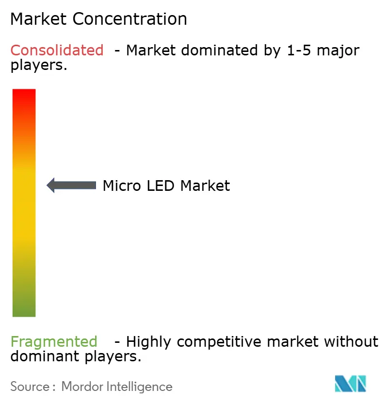
The micro LED market exhibits moderate fragmentation. Samsung, Sony, LG Display, BOE, and AU Optronics collectively control a roughly 45–50% share, relying on vertical integration across epitaxial growth, TFT backplanes, and final assembly. Samsung’s “The Wall Luxury” and LG’s transparent prototypes illustrate incumbent strategies to dominate large-format and specialty niches. BOE and AU Optronics similarly leverage scale to bid for gaming monitor and automotive dash contracts.
Specialist challengers fill performance gaps. VueReal’s solid-print transfer technique claims 99.99% yield for sub-5 µm dies, positioning the firm to supply AR microdisplays. Plessey’s exclusive supply deal with Meta locks the social-media giant into GaN-on-Si roadmaps through 2027. Aledia’s nanowire architecture aims to achieve higher red LED efficiency on eight-inch wafers, potentially disrupting conventional planar designs.
Failure stories temper exuberance. Rohinni’s 2024 closure, despite USD 50 million in funding, underscores capital intensity and yield risks. The lesson sharpens investor due diligence, favoring players with proven mass-transfer or hybrid bonding proficiency. Looking forward, automotive qualification consolidation and hybrid bonding maturation will likely sort contenders from pretenders, gradually concentrating revenue share among the best-capitalized and technologically diversified firms.
Micro LED Industry Leaders
Samsung Electronics Co. Ltd.
Sony Corporation
LG Display Co. Ltd.
BOE Technology Group Co. Ltd.
AU Optronics Corp.
- *Disclaimer: Major Players sorted in no particular order
Micro LED Market Companies Covered in this Report
- Samsung Electronics Co. Ltd.
- Sony Corporation
- LG Display Co. Ltd.
- BOE Technology Group Co. Ltd.
- AU Optronics Corp.
- Epistar Corporation
- PlayNitride Inc.
- Innolux Corporation
- Apple Inc. (LuxVue Technology)
- Tianma Microelectronics Co. Ltd.
- Nichia Corporation
- Sharp Corporation
- VueReal Inc.
- Plessey Semiconductors Ltd.
- Aledia SA
- Ostendo Technologies Inc.
- JBD (Jade Bird Display)
- Leyard Optoelectronics Co. Ltd.
- Seoul Semiconductor Co. Ltd.
- San'an Optoelectronics Co. Ltd.
- Allos Semiconductors GmbH
- Optovate Ltd.
- Foxconn (Hon Hai Precision)

Market Opportunities and Future Outlook
A key whitespace is scaling micro-LED manufacturing onto larger wafer formats and more controllable bonding flows to reduce cost and improve uniformity for high-PPI and fine-pitch products. May to June 2026 produced proof points aligned with that direction, including JBD’s announcement of completion of an upgrade to a 12-inch reconstructed wafer platform for microdisplay mass production and West Lake Yanshan Technology’s start of production at an 8-inch GaN-on-silicon micro-LED IDM facility in Deqing, Zhejiang. These moves correspond to the report’s focus on higher-density near-eye microdisplays (3,000+ PPI) and fine-pitch panels, where mass-transfer yield and pixel-level defect management are decisive.
Opportunity is also developing around module architectures that simplify assembly and increase effective pixel density for deployments beyond prototypes. Planar introduced EverPixel and TruMicro LED technologies in June 2026 using a MicroLED in Package (MIP) architecture, emphasizing packaging-level changes intended to raise subpixel density and improve system-level reliability for professional display installations. The market is simultaneously expanding from display-centric roadmaps into adjacent high-speed optical interconnect applications, supported by 2026 initiatives and partnerships that connect micro-LED emitters with silicon and packaging ecosystems. Overall, larger-wafer manufacturing, investments in hybrid or heterogeneous bonding, and packaging innovations are the most visible pathways for translating micro-LED performance into repeatable, lower-variability supply for wearables, AR microdisplays, automotive display programs, and fine-pitch signage deployments.
Recent Industry Developments in Micro LED Market
- July 2026: BOE reportedly set up a project team focused on micro-LED optical interconnect systems and glass-substrate co-packaged optics (CPO) as part of its push into AI-focused packaging infrastructure. The move extends micro-LED activity beyond displays into data and compute-adjacent applications, broadening the addressable ecosystem for micro-LED emitters and integration know-how.
- June 2026: Planar introduced EverPixel and TruMicro LED technologies built around a MicroLED in Package (MIP) architecture aimed at eliminating LED substrates and increasing RGB subpixel density. The launch highlights packaging and module-level innovation as a near-term lever to improve manufacturability and performance consistency in fine-pitch professional display deployments.
- December 2025: Applied Materials introduced a production-ready hybrid-bonding tool targeting six-inch GaN wafers, with customer qualification slated for Q1 2026. Commercial hybrid-bonding equipment availability supports the industry shift toward wafer-level alignment and throughput improvements needed for high-density microdisplays and other small-format applications.


Micro LED Market Report Scope and Research Methodology
Market Definition and Coverage
The micro-LED market is measured as the revenue generated from micro-scale LED emitters used to build display modules and lighting engines, where the individual LED element is very small and designed for pixel-level control in end products.
Scope exclusions: We exclude mini-LED backlit LCD systems, conventional large LED signage packages, and lab prototypes that do not translate into commercial billings.
Segments Covered in This Report
- By Application
- Smartwatch
- Near-to-Eye Devices (AR/VR)
- Television
- Smartphone and Tablet
- Monitor and Laptop
- Head-up Display
- Digital Signage
- Micro-Projector
- Medical and Surgical Displays
- Industrial Inspection Panels
- By End Use Industry
- Consumer Electronics
- Automotive
- Aerospace and Defense
- Healthcare
- Advertising and Retail
- Industrial and Manufacturing
- Others End Use Industries
- By Panel Size
- Less than 10-inch (Small and Micro-Displays)
- 10- to 50-inch (Medium)
- Above 50-inch (Large)
- By Pixel Pitch
- Fine Pitch (Less than 1.5 mm)
- Standard (1.5 – 2.5 mm)
- Large (Above 2.5 mm)
- By Technology (Color)
- RGB Full-Color
- Monochrome
- By Component
- Epitaxial Wafers
- Backplanes
- Driver ICs
- Transfer and Bonding Equipment
- Inspection and Repair Tools
- By Manufacturing Process
- Mass Transfer
- Epitaxial Wafer Bonding
- Hybrid Bonding
- By Offering
- Display Modules
- Lighting Modules
- By Geography
- North America
- United States
- Canada
- Mexico
- South America
- Brazil
- Argentina
- Rest of South America
- Europe
- United Kingdom
- Germany
- France
- Spain
- Italy
- Rest of Europe
- Asia Pacific
- China
- India
- Japan
- Australia
- South Korea
- Rest of Asia-Pacific
- Middle East and Africa
- Middle East
- Saudi Arabia
- United Arab Emirates
- Turkey
- Rest of Middle East
- Africa
- South Africa
- Kenya
- Rest of Africa
- Middle East
- North America
Data Sources, Market Sizing, and Validation
Desk Research
Desk work starts with pinning down what is being sold and billed across the value chain, and then mapping that to adoption by end-use products. We rely on public sources such as customs and trade statistics, patent publications, peer-reviewed journals on compound semiconductors and display engineering, and standards and guidance notes from bodies such as ISO and IEC (where relevant to testing and safety).
To keep assumptions realistic, we also review company annual reports, investor presentations, and technical white papers, followed by press coverage of pilot lines, capacity additions, and product launches. When needed, paid subscriptions are used for company financials and intelligence, news and financials, patent databases, and selective import-export shipment-level signals to sanity-check directionality. The sources listed here are illustrative, and many other public references were used for collection, validation, and clarification.
Primary Interviews and Surveys
Primary work is used to turn early-stage market signals into a usable model, especially when reported volumes and pricing are not consistently disclosed. We spoke with stakeholders across the supply chain and demand side (component makers, module integrators, equipment ecosystem, and end-use product teams) across the major consuming and manufacturing regions, so our assumptions on yields, pricing steps, and commercialization timing could be challenged and refined.
Distribution of primary research fieldwork respondents
| Company type | Respondent position | Region |
|---|---|---|
| Top tier: 34% | CXOs: 15% | APAC: 43% |
| Mid tier: 48% | Functional/Unit leaders: 32% | EMEA: 36% |
| Smaller Players: 18% | Managers: 53% | Americas: 21% |
Market-Sizing & Forecasting
Sizing starts with a top-down build where production capacity signals, trade flows for relevant components, and expected attach rates by device category are used to reconstruct the addressable demand pool by year. Those totals are then corroborated using selective bottom-up approximations like sampled average selling price (ASP) times shipped units for early commercial display modules, along with channel checks on which applications are actually being billed.
Key inputs used in the model include micro-LED chip and module ASP steps as yields improve, mass-transfer throughput and yield trends, the number of pilot lines moving into volume production, adoption timing in wearables and near-eye displays, and the mix shift between display modules and lighting engines. Since pricing and volumes move quickly in this market, scenario analysis is used for forecasts, and the scenarios are anchored on what interviewees see as the most likely ramp curve by application. Where bottom-up inputs are missing for smaller applications, we fill gaps by applying conservative adoption ratios to the verified demand pool and then re-checking the implied pricing against interview ranges.
Data Validation & Update Cycle
Validation is done through several checks so the totals do not drift away from real market signals. We compare implied units, ASPs, and year-over-year growth rates against independent indicators like capacity announcements, visible product launches, and trade movement patterns, and then investigate outliers before sign-off.
A second analyst review is applied to formulas, unit consistency, and currency conversions, followed by targeted re-contact when a variance is larger than expected or when assumptions conflict across interviews. Reports are refreshed annually, with interim updates when material events occur such as a major ramp delay, a large capacity addition, or a pricing reset. Before delivery, a final pass is completed so clients receive the most current view available.
Mordor Intelligence's Micro Led Market Size Compared With Other Published Estimates
Published market numbers for micro-LED can vary a lot because the market is still moving from pilot to broader commercialization, and the same words are used for different revenue layers. Differences usually come from what is counted (chips only versus modules and engines), which applications are treated as commercial shipments, and whether pricing is assumed to fall quickly as yields improve.
In practice, the spread is often explained by scope decisions, the ramp curve used for wearables and near-eye displays, and how currency timing and inflation are handled for multi-year forecasts. Some estimates also fold in adjacent LED categories or assume a very aggressive expansion into large-area TV volumes, which can lift the headline figure even when supporting shipment signals are limited.
Benchmark comparison
| Source | Market Size | Gaps in Research Methodology |
|---|---|---|
| Mordor Intelligence | USD 0.56 B (2026) | |
| Industry Research Publisher A | USD 1.91 B (2024) | Uses an earlier base year and a much higher growth profile, with limited clarity on whether the value is chips-only, modules, or also adjacent LED categories. This can inflate totals when yields and ASP declines are not constrained by near-term commercialization signals. |
| Global Publisher B | USD 1.84 B (2025) | Shows a very long-range forecast to 2034 with extremely high end-year value, which typically implies aggressive penetration into large-area displays and steep volume ramps that are hard to reconcile with pilot-line throughput and realistic yield progression in the middle years. |
The table shows that most gaps come from what layer of revenue is included and how fast the model assumes the market can ramp into mass production. By separating billed chips, display modules, and lighting engines, and by tying the ramp pace to transfer yield and ASP step-down checks, the estimate stays closer to what can be evidenced year by year, a modeling choice applied by Mordor Intelligence.


Key Questions Answered in the Report
How fast is the micro LED market expected to grow to 2031?
The market is forecast to increase from USD 0.56 billion in 2026 to USD 2.17 billion by 2031, registering a 31.12% CAGR.
Which application segment shows the highest growth potential?
Near-to-eye devices for AR and VR lead with a 32.61% CAGR as headsets demand ultra-bright, high-PPI microdisplays.
Why are driver ICs gaining a larger revenue share?
Integrated driver ICs are essential for per-pixel dimming, adaptive brightness, and UNECE fault-signal compliance, driving a 34.23% CAGR.
Which region dominates manufacturing and revenue?
Asia Pacific holds more than 66% of 2025 revenue, backed by vertically integrated supply chains in Taiwan, China, South Korea and Japan.
What is the main technical barrier to mass adoption?
Sub-10 µm mass-transfer yields remain below 60%, raising costs for high-density panels and delaying widespread AR headset rollout.
How does micro-LED compare with OLED in outdoor visibility?
Micro-LED achieves 4,000–10,000 nits peak brightness versus typical OLED peaks under 1,500 nits, ensuring superior readability in direct sunlight.
Page last updated on:


 Your data is secure and never sold or shared.


