Market Size of Laser Photomask Industry

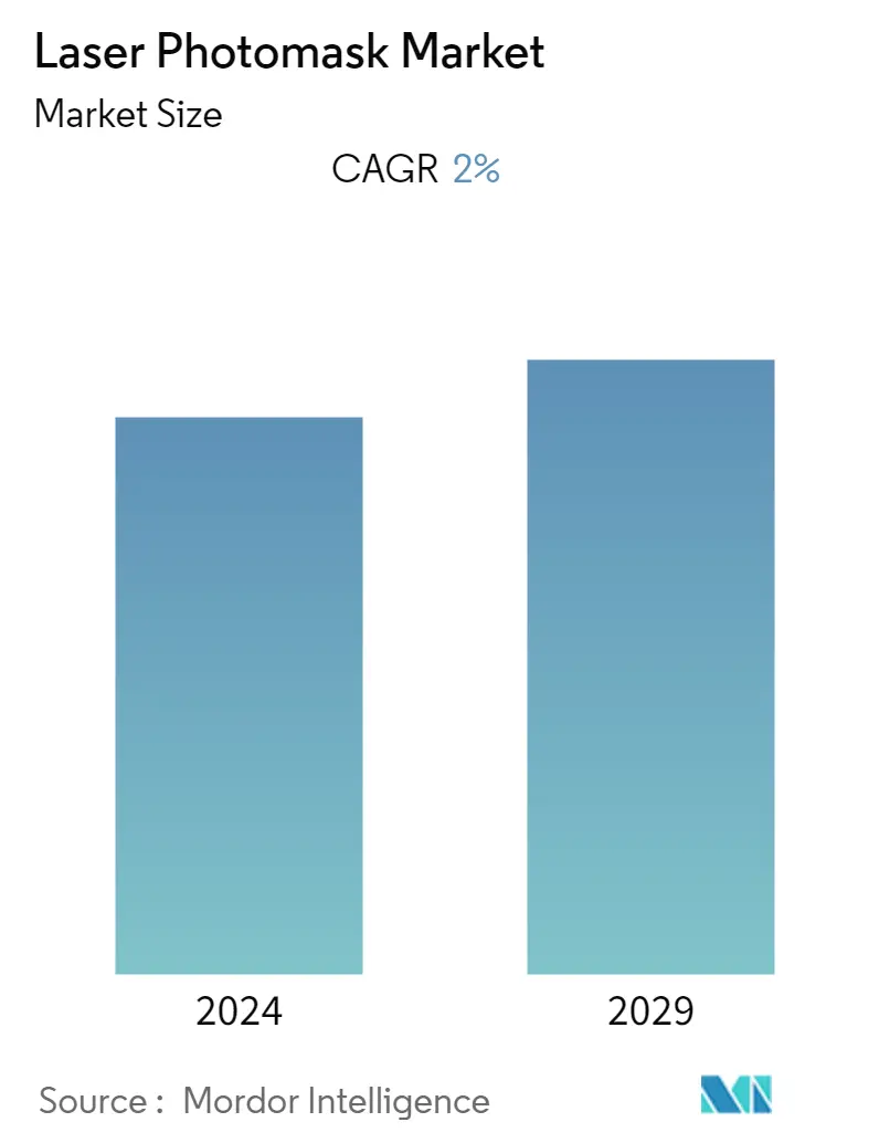
| Study Period | 2019 - 2029 |
| Base Year For Estimation | 2023 |
| Forecast Data Period | 2024 - 2029 |
| CAGR | 2.00 % |
| Fastest Growing Market | Asia Pacific |
| Largest Market | Asia Pacific |
| Market Concentration | Medium |
Major Players
*Disclaimer: Major Players sorted in no particular order |
Laser Photomask Market Analysis
The laser photomask market is expected to record a CAGR over 2% over the forecast period (2021-2026). A photomask is a fused silica plate, covered with a pattern of opaque, transparent, and phase-shifting areas that are projected onto wafers in the lithography process to define the layout of one layer of an integrated circuit.
- As transistors have become smaller and smaller, photomasks have become more complex, to transfer the pattern to silicon wafers accurately. The process of creating photomasks has become correspondingly more advanced, as even slight defects in a photomask can impact the silicon device's performance.
- Verifying that a photomask pattern is defect-free is very critical, especially in the case of high-revenue earning chips. Each chip is the end product in the semiconductor lithography process, with an integral part being the optical lithography that is enabled by a light source. The sources of light used for these photomasks are deep ultraviolet (DUV) and extreme ultraviolet (EUV) light sources.
- With the growing demand for semiconductors with even higher performance for applications, such as big data analysis, artificial intelligence, and the commercialization of driverless car technology, EUV exposure is garnering attention as a next-generation semiconductor manufacturing technology. This trend has significantly driven the production of effective photomasks. Toppan in 2016 developed a next-generation EUV photomask for leading-edge semiconductors. The new photomask minimizes unwanted reflections of light to peripheral sections during EUV exposure, emerging as a next-generation semiconductor manufacturing technology.
Laser Photomask Industry Segmentation
A photomask is a tool used for productions of components, including electronic devices (semiconductors), displays, PCB, and MEMS. It is a master copy for the patterning.
- Electronic devices – Devices, such as CPU and other memory devices that require semiconductor/IC use photomasks.
- Discreet components with a single task – Transistors and memories
- Light receiving/ emitting elements - CCD/CMOS image sensors and LED
- Display devices – LCD and OLED
- MEMS (Micro Electro Mechanical System) - Acceleration sensors
- Magnetic heads for hard disks, among various others.
| By Photomask Type | |
| Reticles | |
| Masters |
| Geography | |
| North America | |
| Europe | |
| Asia-Pacific | |
| Latin America | |
| Middle East & Africa |
Laser Photomask Market Size Summary
The laser photomask market is poised for steady growth, driven by the increasing complexity of photomasks required for advanced semiconductor manufacturing. As transistors shrink in size, the intricacy of photomasks has escalated, necessitating advanced production techniques to ensure defect-free patterns. This precision is crucial for the performance of high-revenue chips, with deep ultraviolet (DUV) and extreme ultraviolet (EUV) light sources playing a pivotal role in the lithography process. The demand for semiconductors, particularly for applications in big data, artificial intelligence, and autonomous vehicle technology, is propelling the adoption of EUV exposure, which is seen as a next-generation manufacturing technology. Companies like Toppan are at the forefront, developing innovative photomasks that minimize light reflection issues during EUV exposure, thereby enhancing semiconductor manufacturing capabilities.
The Asia-Pacific region, particularly China and South Korea, dominates the photomask market due to their robust semiconductor industries and the presence of major electronics manufacturers. The rising demand for electronic devices in developing countries, fueled by increasing disposable incomes and a burgeoning middle class, further propels the market. China's strategic policy changes to bolster its domestic semiconductor industry and the influence of trade fairs like Photomask Japan contribute to the region's market growth. The competitive landscape is marked by strategic mergers and acquisitions, as seen with KLA-Tencor's agreement to acquire Orbotech, and product innovations like Heidelberg Instruments' ULTRA Semiconductor Laser Mask Writer, which addresses diverse semiconductor applications.
Laser Photomask Market Size - Table of Contents
-
1. MARKET DYNAMICS
-
1.1 Market Overview
-
1.2 Introduction to Market Drivers and Restraints
-
1.3 Market Drivers
-
1.3.1 Increasing Use of Electronic Devices
-
1.3.2 Advent of Technologies, such as Big Data and AI
-
-
1.4 Market Restraints
-
1.4.1 Complexity in Fabrication
-
-
1.5 Industry Attractiveness - Porter's Five Forces Analysis
-
1.5.1 Threat of New Entrants
-
1.5.2 Bargaining Power of Buyers/Consumers
-
1.5.3 Bargaining Power of Suppliers
-
1.5.4 Threat of Substitute Products
-
1.5.5 Intensity of Competitive Rivalry
-
-
-
2. MARKET SEGMENTATION
-
2.1 By Photomask Type
-
2.1.1 Reticles
-
2.1.2 Masters
-
-
2.2 Geography
-
2.2.1 North America
-
2.2.2 Europe
-
2.2.3 Asia-Pacific
-
2.2.4 Latin America
-
2.2.5 Middle East & Africa
-
-
Laser Photomask Market Size FAQs
What is the current Laser Photomask Market size?
The Laser Photomask Market is projected to register a CAGR of 2% during the forecast period (2025-2030)
Who are the key players in Laser Photomask Market?
KLA-Tencor Corporation, Applied Materials Inc., Photronics Inc., Nippon Filcon Co. Ltd and Toppan Printing Co. Ltd are the major companies operating in the Laser Photomask Market.

