
Japan Flash Memory Market Size and Share
Market Overview
| Study Period | 2020 - 2031 |
|---|---|
| Forecast Data Period | 2026 - 2031 |
| Base Year Market Size (2025) | USD 3.16 Billion |
| Market Size (2026) | USD 3.25 Billion |
| Market Size (2031) | USD 3.75 Billion |
| Growth Rate (2026 - 2031) | 2.90 % |
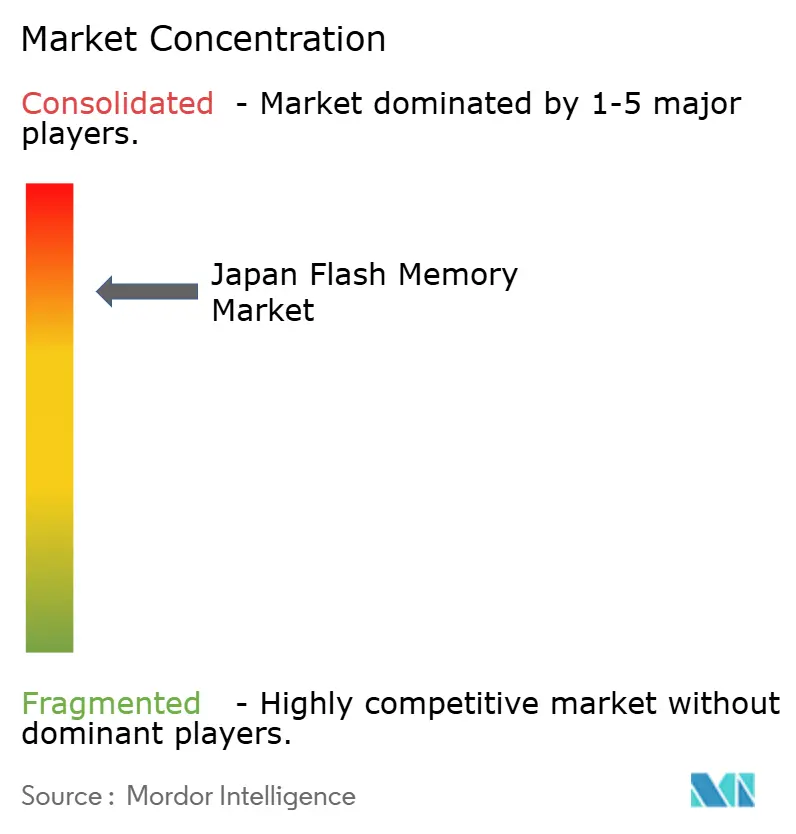
| Market Concentration | High |
Major Players *Disclaimer: Major Players sorted in no particular order Image © Mordor Intelligence. Reuse requires attribution under CC BY 4.0. | |
Japan Flash Memory Market Analysis by Mordor Intelligence
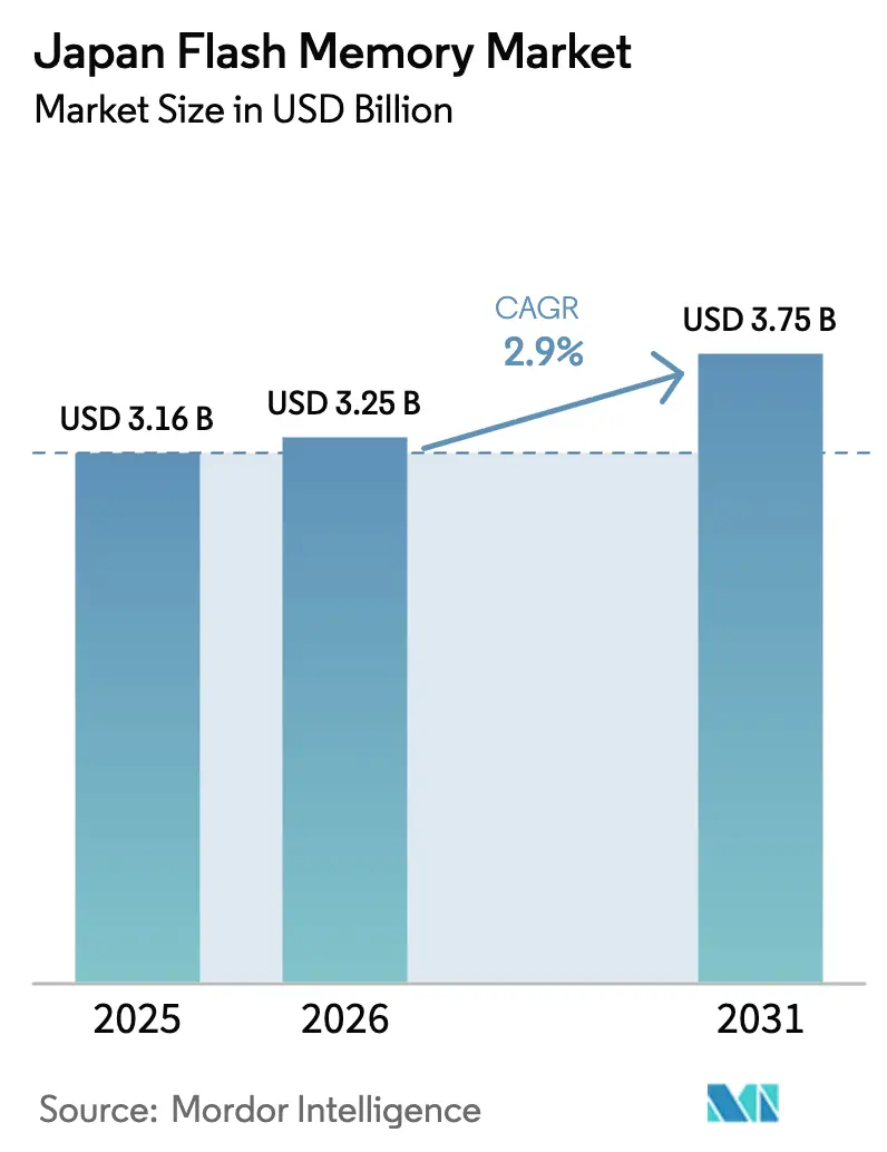
Japan flash memory market size in 2026 is estimated at USD 3.25 billion, growing from 2025 value of USD 3.16 billion with 2031 projections showing USD 3.75 billion, growing at 2.90% CAGR over 2026-2031. Government incentives, a disciplined capacity-expansion roadmap, and the migration of data-center and automotive workloads to high-performance solid-state storage underpin this steady climb. At the same time, cyclical pricing swings and rising energy costs temper near-term profitability, especially for fab operators exposed to spot NAND quotations. Technology leadership in 218-layer and higher 3D NAND nodes enables cost reduction that offsets part of the pricing pressure, while emerging non-volatile memory formats such as MRAM begin to capture industrial sockets that demand extreme endurance. Vertically integrated producers that own both wafer output and module assembly secure better margins than pure-play assemblers. As a result, the Japan flash memory market continues to consolidate around a handful of scale players that can fund the transition to 300-layer architectures.
Key Report Takeaways
- By memory type, 3D NAND led with 48.45% of the Japan flash memory market share in 2025 while emerging MRAM and other non-volatile memories are forecast to post the fastest growth at a 4.05% CAGR to 2031.
- By density, the 64 Gb–256 Gb band accounted for 37.15% of revenue in 2025 of the Japan flash memory market; the 512 Gb-and-above tier is set to expand at a 3.62% CAGR through 2031.
- By interface, PCIe/NVMe SSDs captured 42.25% revenue share in 2025 of the Japan flash memory market, and Universal Flash Storage is projected to rise at a 3.90% CAGR on accelerating automotive uptake.
- By end user, mobile and tablets held 38.20% revenue in 2025 of the Japan flash memory market, while automotive applications are projected to grow at a 3.82% CAGR through 2031.
Note: Market size and forecast figures in this report are generated using Mordor Intelligence’s proprietary estimation framework, updated with the latest available data and insights as of 2026.
Japan Flash Memory Market Trends and Insights
Drivers Impact Analysis*
| Driver | (~) % Impact on CAGR Forecast | Geographic Relevance | Impact Timeline |
|---|---|---|---|
| Surging adoption of SSDs in consumer and enterprise PCs | +0.6% | Kanto, Kansai (enterprise hubs) | Medium term (2-4 years) |
| Expanding smartphone production with higher on-board storage | +0.5% | Kanto, Kansai (design centers), Kyushu (assembly) | Short term (≤ 2 years) |
| Rapid growth of automotive ADAS and in-vehicle infotainment | +0.7% | Chubu, Kyushu (automotive clusters) | Long term (≥ 4 years) |
| Proliferation of IoT edge devices needing local flash storage | +0.4% | National, with concentration in Kanto industrial zones | Medium term (2-4 years) |
| Government incentives for domestic advanced-flash fabs | +0.5% | Tohoku, Kyushu, Hokkaido (fab sites) | Long term (≥ 4 years) |
| 3D NAND use in metaverse-related Japanese wearables | +0.2% | Kanto (Tokyo metro), Kansai (Osaka metro) | Medium term (2-4 years) |
| Source: Mordor Intelligence | |||
Surging Adoption of SSDs in Consumer and Enterprise PCs
Enterprise refresh cycles are shifting decisively toward NVMe storage, which delivers single-digit microsecond latency, thereby reducing rack footprints and power draw in data center clusters located in Tokyo and Osaka.[1]Western Digital Newsroom, “Western Digital Introduces New Datacenter SSD Portfolio Built on 218-Layer BiCS Flash,” westerndigital.com Notebook makers are mirroring this shift as PCIe Gen4 drives become mainstream in mid-range systems. Western Digital’s 218-layer BiCS devices now ship in volume, providing 3 drive writes per day endurance for finance and public-sector workloads. Consumer adoption is accelerating as the 5G rollout drives the need for local caching in routers and base stations. Together, these factors add 0.6 percentage points to overall growth, with peak influence expected between 2026 and 2028.
Expanding Smartphone Production with Higher On-Board Storage
Premium handsets from Sony, Sharp, and Kyocera feature 256 GB and 512 GB storage, enabling 4K video capture and AI-driven imaging.[2]Sony Press Team, “Xperia 1 VI Launch Product Specifications and Features,” sony.com Apple retains a commanding share, but local brands keep niche segments that value ruggedization and high-resolution cameras. Fifth-generation wireless penetration already covers more than half the subscriber base, driving photo and video file sizes higher. These trends deliver a 0.5 percentage-point uplift to the long-term CAGR.
Rapid Growth of Automotive ADAS and In-Vehicle Infotainment
Domestic automakers integrate Level 2+ driver-assistance suites that buffer lidar, radar, and camera data locally on flash modules certified to AEC-Q100 standards. Kioxia’s UFS 4.0 devices supply 4,200 MB/s read throughput, enabling real-time sensor fusion.[3]Kioxia Technical Briefs, “BiCS Flash Roadmap and Market Outlook,” kioxia.com Infotainment head units shift from 32 GB eMMC to 128 GB UFS to accommodate over-the-air map updates and high-definition cockpit displays. The automotive pivot contributes 0.7 percentage points to market expansion and extends beyond 2028 as semi-autonomous functions become widespread.
Government Incentives for Domestic Advanced-Flash Fabs
Tokyo allocated JPY 243 billion in direct subsidies to the Kioxia-Western Digital venture and lined up another JPY 150 billion for next-generation memory R&D.[4]METI, “Comprehensive Semiconductor Strategy,” meti.go.jp Micron committed JPY 500 billion to its Hiroshima site, anchoring a new regional supply cluster. These incentives lower effective capital intensity, allow Japanese fabs to match Korean layer counts, and add 0.5 percentage points to the growth trajectory.
Restraints Impact Analysis*
| Restraint | (~) % Impact on CAGR Forecast | Geographic Relevance | Impact Timeline |
|---|---|---|---|
| Cyclical NAND price volatility and inventory gluts | -0.5% | National, affecting all fab operators | Short term (≤ 2 years) |
| Reliability challenges at sub-1z-nm nodes | -0.3% | Kanto, Kansai (R&D centers), Tohoku (pilot lines) | Medium term (2-4 years) |
| High domestic energy costs pressuring fab economics | -0.4% | National, acute in Kyushu and Tohoku | Long term (≥ 4 years) |
| Supply risk of high-purity HF and photo-resist chemicals | -0.2% | National, with upstream concentration in Chubu and Kanto | Medium term (2-4 years) |
| Source: Mordor Intelligence | |||
Cyclical NAND Price Volatility and Inventory Gluts
Contract prices fell 6.2% quarter on quarter in 4Q 2024 and are forecast to dip another 10-15% in 1Q 2025 before a modest rebound. Fab operators face margin compression just as new capacity ramps. Kioxia flagged 90 days of inventory in its IPO prospectus, exposing it to further markdowns. This pricing whiplash subtracts 0.5 percentage points from the projected CAGR and complicates cash-flow planning through 2026.
High Domestic Energy Costs Pressuring Fab Economics
Japan’s grid relies on imported liquefied natural gas, pushing electricity tariffs above those of peer manufacturing hubs. Kioxia alone consumes more than 1 TWh annually across its Yokkaichi and Kitakami sites, prompting the company to set a target of sourcing 30% renewable power by 2030. Micron’s Hiroshima expansion will add another 200 MW load to regional transmission networks. Elevated energy costs shave 0.4 percentage points from growth through the forecast horizon.
*Our forecasts treat driver/restraint impacts as directional, not additive. The impact forecasts reflect baseline growth, mix effects, and variable interactions.
Segment Analysis
By Memory Type: 3D NAND Consolidates, MRAM Accelerates
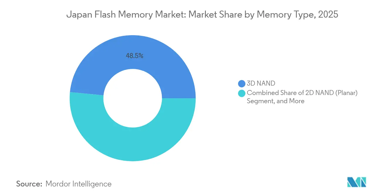
3D NAND captured 48.45% revenue in 2025 on the back of data-center conversions to all-flash arrays and automotive adoption of UFS 4.0 modules. This share anchors the Japan flash memory market through the forecast, with density scaling beyond 218 layers keeping average selling prices competitive. Samsung and SK hynix push toward 300-layer devices, putting cost pressure on incumbents yet widening the total addressable pool as terabyte-class packages proliferate.
Other non-volatile technologies, chiefly MRAM and ReRAM, are forecast to expand at a 4.05% CAGR as automotive and industrial equipment require instant-on capability and million-cycle endurance. Kioxia’s OCTRAM crosspoint design, co-developed with SK hynix, underpins this surge. NOR and planar NAND linger in legacy designs but cede ground as vertical stacking shrinks die costs. These dynamics keep the Japan flash memory market diversified yet tilted toward 3D structures over the forecast window.


By Density: 512 Gb-Plus Tiers Climb
The 64 Gb–256 Gb class held 37.15% revenue in 2025, tied to smartphone bills of materials that favor 128 GB and 256 GB capacities. Rising photo and video file sizes, combined with carrier bundling of unlimited data, nudge consumers toward higher SKUs.
The 512 Gb-and-above bracket is projected to grow at a 3.62% CAGR, lifting the Japan flash memory market size for this density group as AI edge devices and ADAS platforms embed 1 TB storage modules. Kioxia’s new 2 Tb QLC die enables single-package 1 TB UFS parts, accelerating the migration. Lower-density tiers remain vital for microcontrollers and IoT sensors where energy efficiency and tiny footprints outweigh raw capacity.
By Interface / Form Factor: UFS Gains Traction
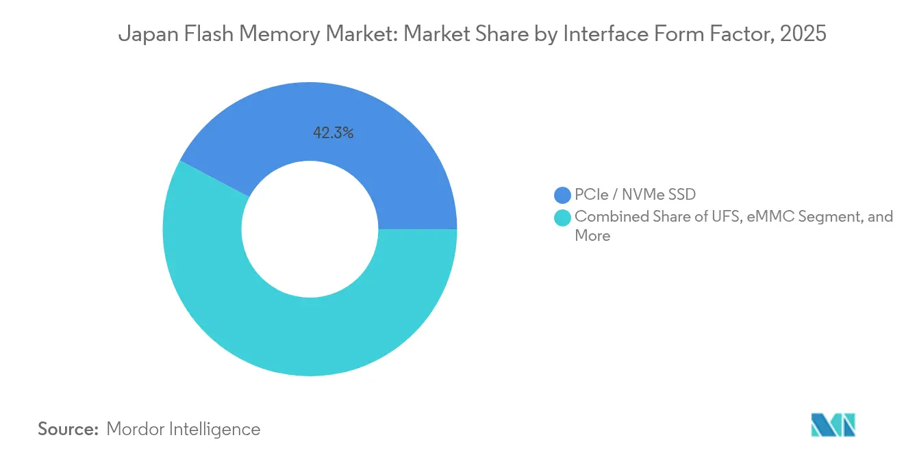
PCIe/NVMe SSDs delivered 42.25% revenue in 2025 thanks to enterprise rollouts that prioritize throughput and latency. Japan’s hyperscalers retired SATA enclosures in favor of Gen4 and Gen5 NVMe units, locking in performance headroom for AI inference.
Universal Flash Storage is forecast to log the fastest interface growth at 3.90% CAGR as automotive platforms mandate high-speed managed flash with automotive-grade temperature tolerance. eMMC persists in cost-sensitive IoT endpoints, while SATA fades except for niche industrial refreshes. These trends force controller vendors to integrate both NVMe and UFS host compliance into future chipsets, broadening serviceable applications for the Japan flash memory market.
By End User Application: Automotive Outpaces Handsets
Smartphones and tablets accounted for 38.20% of the revenue in 2025, supported by steady premium phone refreshes. The Japan flash memory market size allocated to automotive is, however, forecast to expand at a 3.82% CAGR between 2026 and 2031, overtaking client PCs as the second-largest consumption vertical.
Level 2+ ADAS systems cache multi-sensor data locally, while infotainment head units store HD maps and OTA firmware. Data centers absorb the highest endurance SSDs to serve AI inference workloads that demand a consistent quality of service. Industrial and IoT nodes continue to specify eMMC and low-density UFS where absolute reliability is paramount.
Geography Analysis
Kanto remains the largest contributor to the Japan flash memory market, anchored by Tokyo’s concentration of headquarters and research labs for Kioxia, Sony Semiconductor, and Renesas. Western Digital maintains a major architecture center in Yokohama, collaborating with Kioxia on CXL-enabled memory fabrics. Shin-Etsu expands photoresist output in nearby Gunma, guaranteeing material supplies for local fabs. This cluster effect compresses design-cycle times and sustains the region’s leadership position.
Kyushu is expected to be the fastest-growing area through 2030. TSMC’s Kumamoto facility has already begun production of 28 nm and 16 nm nodes and plans to build a second fab for 7 nm nodes by 2027. Kyushu also hosts photoresist and chemical producers that supply both JASM and Kioxia, creating a supply chain reminiscent of Taiwan’s Hsinchu hub. Proximity to Korean fabs shortens logistical lead times for wafer starts and die shipments.
Tohoku houses Tokyo Electron equipment plants and PSMC’s Sendai line for embedded flash microcontrollers. Chubu generates strong demand through Toyota, Honda, and Denso, which integrate UFS 4.0 modules into new ADAS architectures. Kansai supports Panasonic and Rohm with power-management device fabs embedding on-chip flash. Hokkaido prepares for Rapidus’ 2 nm logic facility adjacent to planned memory-packaging lines. Chugoku and Shikoku remain smaller contributors yet benefit from spillover as the Kyushu complex expands.
Regulatory Landscape
Japan's flash memory market is shaped by industrial policy and export controls, with the Ministry of Economy, Trade and Industry (METI) administering semiconductor revitalization measures and targeted subsidies for advanced manufacturing and R&D. The policy stance includes direct support packages tied to domestic production and technology upgrades, highlighted by METI backing for large-scale memory investments such as Micron's Hiroshima expansion support announced in July 2026, which reinforces scrutiny around domestic capability building and supply resilience.
For compliance, flash memory suppliers and device OEMs operate within Japan's export control regime aligned with the Wassenaar Arrangement, alongside product and data obligations that affect downstream deployment of storage in connected devices and data centers. Cross-industry requirements such as the Act on Protection of Personal Information (APPI) and cybersecurity-related frameworks influence enterprise storage qualification, while materials and environmental compliance (for example, chemical handling under CSCL and RoHS-aligned substance controls) adds governance overhead across wafer fabs, assembly, and electronics manufacturing.
Value Chain Analysis
Japan's flash memory value chain runs from upstream materials and equipment through wafer fabrication, controller and firmware design, module assembly and packaging, qualification, and distribution into end markets including mobile, automotive, industrial, and data center storage. At the fabrication core, Kioxia and Sandisk (formerly SanDisk) operate long-running NAND flash joint venture manufacturing at Yokkaichi and Kitakami, anchoring domestic wafer output and node transitions, with process architectures such as CMOS directly Bonded to Array (CBA) at Kitakami Fab2 illustrating how integration of logic and memory process steps supports density scaling and cost improvements.
Downstream value capture is increasingly concentrated among firms that can couple die supply with reference designs and qualification for automotive and enterprise use cases. Micron's Hiroshima operations underscore the role of local sourcing and supplier ecosystems, including reliance on Japanese materials providers, while Western Digital maintains a Japan R&D footprint and links it to joint manufacturing with Kioxia for NAND-based products. Logistics and customer enablement are reinforced by local OEM clusters in automotive, electronics, and hyperscale IT, where long qualification cycles and endurance and temperature requirements elevate test, validation, and firmware tuning as differentiators beyond raw bit supply.
Competitive Landscape
Kioxia and Western Digital jointly operate Japan’s largest 3D NAND capacity at Yokkaichi and Kitakami, giving them scale advantages in die output and yield learning. Samsung and SK hynix defend technological leadership with 290-layer and 321-layer stacks, compelling local rivals to accelerate R&D spending. Micron’s Hiroshima expansion underscores a commitment to the Japan flash memory market and aims to win automotive and industrial sockets that prize endurance.
Renesas, Sony Semiconductor, and Panasonic focus on embedded flash for microcontrollers, image sensors, and specialized industrial modules, where reliability outweighs the cost of gigabytes. Controller designers Phison and Silicon Motion integrate AI-driven error correction, extending the life cycles of QLC-based SSDs and adding differentiation beyond raw NAND supply. Startups targeting MRAM and ReRAM exploit whitespace opportunities that require over one million-cycle endurance for factory automation workloads.
Regulatory subsidies reduce capital intensity but also heighten scrutiny on sovereign resilience and supply-chain security. The market structure favors vertically integrated players that can self-qualify wafers, controllers, and finished drives. Standards progress on UFS 4.0 and PCIe Gen5 accelerates commoditization at the interface layer, pushing value capture toward core IP in cell structure and firmware algorithms within the Japan flash memory market.
Japan Flash Memory Industry Leaders
Western Digital Corp
Micron Technology Inc.
Renesas Electronics Corporation
Kioxia Holdings Corporation
GigaDevice Semiconductor Inc.
- *Disclaimer: Major Players sorted in no particular order

Market Opportunities and Future Outlook
Domestic semiconductor policy and large, visible investment programs create whitespace for suppliers that can localize advanced flash manufacturing, materials, and enabling IP in Japan. METI's ongoing semiconductor strategy, including a national ambition cited in 2026 reporting to raise domestically produced semiconductor sales to JPY 40 trillion by 2040, supports multi-year demand for fab equipment, specialty chemicals, and qualified supply chains serving memory makers and their downstream module ecosystems.
On the demand side, opportunities cluster where performance and reliability requirements lift content per system, especially AI-driven storage refresh cycles in data centers and automotive-grade managed flash. In 2026, Kioxia disclosed a growth investment posture for the AI inference era, including capex and R&D emphasis, and together with Sandisk started production of 10th-generation 3D flash at Kitakami Fab2, signaling ecosystem pull for advanced 3D NAND supply, controllers, and packaging services. Micron's July 2026 Hiroshima expansion initiative, backed by METI support, also reinforces build-out of advanced memory capacity in Japan, expanding adjacent opportunities in power, test, and high-reliability component supply that connects memory output to automotive and enterprise platforms.
Recent Industry Developments
- July 2026: Micron Technology Inc. broke ground on a 1.5 trillion yen expansion of its manufacturing facility in Hiroshima Prefecture. The development expands Japan's capacity for high-end memory production, reinforcing its role as a strategic hub and reshaping regional supply chains. The investment underlines Micron's commitment to automotive and industrial memory applications in the Japanese market.
- July 2026: Kioxia Holdings Corporation (with Sandisk/SanDisk) commenced production of 10th-generation 3D flash memory at Fab2 (K2) in the Kitakami Plant. The move accelerates AI optimized memory capacity in Japan and strengthens the Kioxia SanDisk joint venture footprint across the Kitakami facility. This expansion supports demand for high density NAND in enterprise and automotive applications.
- June 2026: Kioxia Holdings Corporation announced growth investment strategy allocating ~470 billion yen to capex and ~230 billion yen to R and D over three years. The plan signals aggressive scaling and a push into 218/300+ layer NAND ecosystems to meet AI era memory demand. The increased capital outlay aims to improve process maturity and maintain leadership in advanced memory nodes.


Research Methodology Framework and Report Scope
Market Definition and Coverage
For this report, the market covers revenue generated from flash memory sold and used in Japan across key end uses such as consumer devices, PCs and storage, industrial electronics, automotive electronics, and data center storage.
Scope exclusions: We exclude DRAM and other non-flash memory types, and we do not count downstream device value, services, or software.
Segmentation Overview
- By Memory Type
- 3D NAND
- 2D NAND (Planar)
- NOR Flash
- Other Memory Type
- By Density
- Up to 256 Mb
- 512 Mb – 2 Gb
- 4 Gb – 32 Gb
- 64 Gb – 256 Gb
- 512 Gb and Above
- By Interface / Form Factor
- eMMC
- UFS
- SATA SSD
- PCIe / NVMe SSD
- SPI NOR
- USB Flash and Removables
- By End User Application
- Data Center and Enterprise Servers
- Mobile and Tablets
- Automotive (ADAS, Infotainment)
- Industrial and IoT Devices
- Client Computing (PC, Laptop, Client SSD)
- Consumer Electronics (Gaming, Wearables)
- Other End User Application
Data Sources, Market Sizing, and Validation
Desk Research
Desk research starts with building the demand and supply context that can be checked using public records. We typically refer to sources such as Japan Customs trade statistics, METI industrial statistics, Statistics Bureau of Japan releases, OECD and World Bank macro indicators, and relevant publications from IEEE and other peer reviewed journals to understand shipments, production signals, and technology shifts.
After that, we use company annual reports, investor presentations, earnings call transcripts, and trusted press coverage to map capacity additions, product mix changes, and exposure to end markets like data centers and automotive. Where available, our analysts also use paid subscriptions for company financial intelligence, patent databases, and shipment level trade data to support cross checks on volumes and pricing trends. The sources listed here are illustrative, and many additional references were used to collect, validate, and clarify the data points during the work.
Primary Interviews and Surveys
Primary work is used to pressure test desk assumptions that often vary by application, pricing cycle, and node transitions. We spoke with a mix of semiconductor ecosystem participants in Japan, including manufacturers, component distributors, OEM procurement teams, and domain specialists who track storage demand in data center, consumer electronics, and automotive programs. These inputs were used to confirm ASP direction, mix shifts between NAND and NOR, and realistic adoption timing by end use.
Distribution of primary research fieldwork respondents
| Company type | Respondent position |
|---|---|
| Top tier: 28% | CXOs: 12% |
| Mid tier: 50% | Functional/Unit leaders: 28% |
| Smaller Players: 22% | Managers: 60% |
Market-Sizing & Forecasting
Sizing starts from a top-down build where demand pools in Japan are reconstructed using electronics production and trade signals, storage shipment indicators, and end use adoption patterns. Once this first cut is formed, it is cross checked with selective bottom-up approximations, such as sampled supplier revenue splits, channel feedback on shipment run rates, and ASP times volume sanity checks for key use cases.
A few inputs that usually matter a lot for flash memory were tracked closely, including NAND price cycle direction, client and enterprise SSD attachment rates, smartphone and PC unit trends, automotive electronics content growth, and data center storage refresh intensity. For forecasting, we mainly use scenario analysis supported by simple time series checks, so cyclical pricing and recovery timing can be reflected without overfitting. If a sub segment has sparse data, assumptions are bridged using the closest comparable end use signals, then revalidated through interviews before totals are finalized.
Data Validation & Update Cycle
Outputs are validated through multiple checks so unusual jumps do not slip through. We compare model totals against independent signals like trade movement, reported capacity changes, and end market shipment trends, and then investigate variances that do not match the pricing cycle or demand story.
Before sign off, the work is reviewed in steps, and follow up outreach is triggered when gaps appear in ASP movement, product mix, or end use allocation. Reports are refreshed annually, and interim updates are made when major events occur that can change pricing, supply, or demand. Right before delivery, a final review pass is completed so clients receive the latest updated view.
Mordor Intelligence's Japan Flash Memory Market Size Versus Other Published Estimates
Published market sizes for Japan flash memory can differ because not every publisher counts the same memory types, the same demand points, or the same pricing basis for revenue. Differences also come from how fast pricing assumptions are refreshed in a market that moves in cycles.
Some published figures fold broader semiconductor memory revenue into the total, or they apply a price path that is not tied back to shipment signals. The split is usually explained by scope and refresh cadence, since Mordor Intelligence counts only flash memory revenue in Japan and keeps the model anchored to application level demand checks and current pricing direction.
Benchmark comparison
| Source | Market Size | Gaps in Research Methodology |
|---|---|---|
| Mordor Intelligence | USD 3.16 B (2025) | |
| Global Consultancy A | USD 3.72 B (2024) | Uses a wider memory definition at the country level and may include DRAM within a combined memory chip total, which lifts the Japan value versus a flash-only cut. |
| Industry Publisher B | USD 4.58 B (2025) | Often includes adjacent module level value and applies a smoother, optimistic ASP progression, which can overstate revenue during down cycle or early recovery years. |
The benchmark spread is mainly linked to what is included in the revenue pool and how pricing is carried forward year to year. By keeping the estimate traceable to flash-only demand drivers, realistic unit signals, and clearly stated pricing assumptions, the final number stays easier to replicate and to use for planning.


Key Questions Answered in the Report
How large is the Japan flash memory market in 2026?
The Japan flash memory market size reaches USD 3.25 billion in 2026 and is on track for USD 3.75 billion by 2031.
What is the expected CAGR for Japanese flash memory through 2031?
Aggregate revenue is projected to grow at a steady 2.90% CAGR across the 2026-2031 forecast window.
Which application is the fastest-growing consumer of flash memory in Japan?
Automotive electronics, especially Level 2+ ADAS and infotainment systems, are set to expand at a 3.82% CAGR to 2031.
Which interface technology is rising quickest in Japanese flash storage?
Universal Flash Storage is projected to grow at a 3.90% CAGR as automotive and mobile devices adopt UFS 3.1 and UFS 4.0 modules.
How are government incentives affecting domestic flash manufacturing?
Subsidies exceeding JPY 243 billion reduce capital intensity for new fabs and add 0.5 percentage points to long-term market growth.
Page last updated on:


 Your data is secure and never sold or shared.


