Market Size of Indium Phosphide Wafer Industry

| Study Period | 2019 - 2029 |
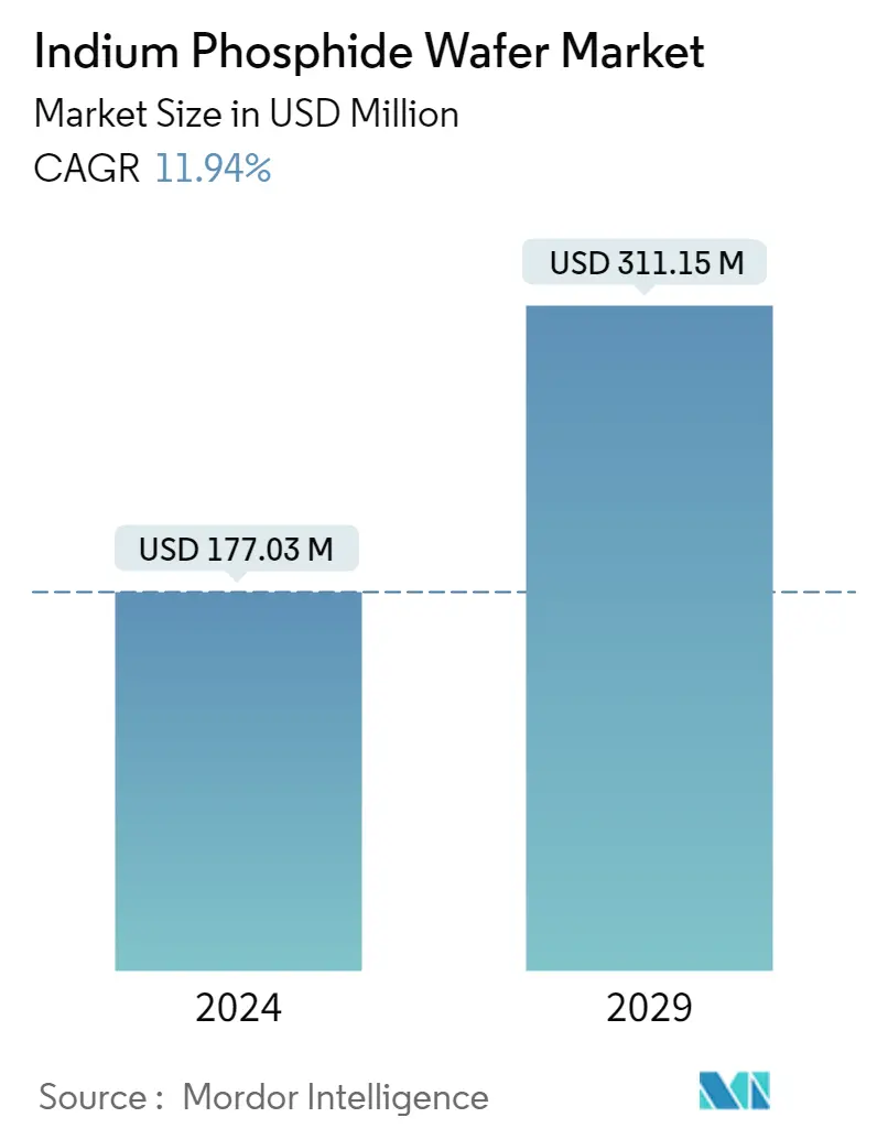
| Market Size (2024) | USD 177.03 Million |
| Market Size (2029) | USD 311.15 Million |
| CAGR (2024 - 2029) | 11.94 % |
| Fastest Growing Market | Asia-Pacific |
| Largest Market | Asia-Pacific |
| Market Concentration | Low |
Major Players
*Disclaimer: Major Players sorted in no particular order |
Indium Phosphide Wafer Market Analysis
The Indium Phosphide Wafer Market size is estimated at USD 177.03 million in 2024, and is expected to reach USD 311.15 million by 2029, growing at a CAGR of 11.94% during the forecast period (2024-2029).
Indium phosphide (InP) has properties that produce highly efficient lasers, modulators, and sensitive photodetectors. It can also generate laser signals and convert and identify those signals back to the electronic form. These are used for company networks and data centers, long-haul optical fiber connections over far distances, wireless connections for 3G, 5G, and LTE base stations, and satellite communication. The growth in such requirements is driving the market.
- Indium phosphide wafers are increasingly adopted in the manufacture of LiDAR for automotive, 3D sensing, consumer wearables, and the growth in datacom in the telecommunication sector. This is expected to drive the market during the forecast period. In addition, some of the major applications of InPinclude 5G communications, data center connectivity that uses lights and lasers, fiber optic lasers and detectors, silicon photonics, RF amplifiers, and switches used in military and 5G communications, and infrared thermal imaging in health.
- Electronic components known as optoelectronic devices detect and regulate light. They convert electrical information into infrared or visible energy and vice versa. It is utilized in photovoltaic power supply, optical fiber communication systems, monitor and control circuits, and electric eyes. Optoelectronic components are used in quantum cascade lasers and injection laser diodes for stimulated emission. LEDs and image sensors are utilized in digital imaging systems, packaging, and safety applications.
- According to the Ericsson Mobility Report published in November 2020, the global mobile data traffic was estimated to reach around 51 EB (exabytes) per month by the end of 2020. This was projected to grow by a factor of almost 4.5 to reach 226 EB per month in 2026. This figure represents the mobile data that will be consumed by greater than 6 billion people using smartphones, laptops, and a multitude of new devices at a time.
- The semiconductor silicon wafer serves as the foundation of the electronics industry and is the main component of many microelectronic devices. With the current advances in the technology landscape, electronic mobility, and digitalization, these items are finding use in a wide range of devices. The requirement for additional capability from a single device has also grown dramatically as a result of the need for small-sized gadgets, which boosts the price of the silicon wafer.
- The COVID-19 pandemic has halted the manufacturing of several items in the semiconductor production equipment industry owing to the continued lockdown in most regions across the world. Lockdown measures reduced the demand for consumer electronic gadgets, which had a global impact on the semiconductor sector. The continued decline in worldwide demand and export shipments for automobiles caused a negative impact on the semiconductor market, which is currently slowing down the demand for semiconductor manufacturing equipment.
Indium Phosphide Wafer Industry Segmentation
Indium phosphide, a binary semiconductor, is used to create indium phosphide wafers. It provides a better electron velocity than most common semiconductors, including silicon. Hence, it is the most practical compound for optoelectronic applications, fast transistors, and resonance tunneling diodes.
The scope of the study focuses on the market analysis of indium phosphide wafer products sold across the globe. The market sizing encompasses the revenue generated through indium phosphide wafer products sold by various market players. The study also tracks key market parameters, underlying growth influencers, and major vendors operating in the industry, which supports market estimations and growth rates over the forecast period. The study further analyzes the overall impact of the COVID-19 pandemic on the ecosystem. The scope of the report encompasses market sizing and forecast for segmentation by diameter, end-user industry application, and geography.
| By Diameter | |
| 50.8 mm or 2 " | |
| 76.2 mm or 3 " | |
| 100 mm or 4" and Above |
| By End-user Industry Application | |
| Consumer Electronics | |
| Telecommunications | |
| Medical | |
| Other End-user Industry Applications |
| By Geography | |
| North America | |
| Europe | |
| Asia-Pacific | |
| Rest of the world |
Indium Phosphide Wafer Market Size Summary
The Indium Phosphide (InP) wafer market is poised for significant growth, driven by its applications in high-efficiency lasers, modulators, and photodetectors. These wafers are integral to advanced communication technologies, including 3G, 5G, and LTE networks, as well as satellite communications and long-haul optical fiber connections. The increasing demand for data centers and wireless connectivity solutions is a key factor propelling market expansion. Additionally, the adoption of InP wafers in LiDAR technology for automotive and 3D sensing applications further underscores their growing importance. The market is also benefiting from the rise of wearable technology and the expanding telecommunication sector, which relies on InP for data center connectivity and silicon photonics.
The competitive landscape of the InP wafer market is characterized by the presence of major manufacturers such as JX Nippon Mining & Metals Corporation and Powerway Advanced Material Co. Ltd, which significantly influence market dynamics. The Asia-Pacific region, with its robust semiconductor foundries, plays a pivotal role in the market's growth. Countries like Taiwan, South Korea, Japan, and China are at the forefront, with China making substantial investments to enhance its semiconductor capabilities. The market is further bolstered by strategic partnerships and technological advancements, such as those seen in the Photonic Integrated Circuit platforms. These developments, alongside significant investments in semiconductor and photonics industries globally, are expected to intensify competitive rivalry and drive the market forward during the forecast period.
Indium Phosphide Wafer Market Size - Table of Contents
-
1. MARKET INSIGHTS
-
1.1 Market Overview
-
1.2 Industry Attractiveness - Porter's Five Forces Analysis
-
1.2.1 Bargaining Power of Suppliers
-
1.2.2 Bargaining Power of Buyers/Consumers
-
1.2.3 Threat of New Entrants
-
1.2.4 Threat of Substitute Products
-
1.2.5 Intensity of Competitive Rivalry
-
-
1.3 Industry Value Chain Analysis
-
1.4 Technology Snapshot
-
1.5 Assessment of the Impact of COVID-19 on the Industry
-
-
2. MARKET SEGMENTATION
-
2.1 By Diameter
-
2.1.1 50.8 mm or 2 "
-
2.1.2 76.2 mm or 3 "
-
2.1.3 100 mm or 4" and Above
-
-
2.2 By End-user Industry Application
-
2.2.1 Consumer Electronics
-
2.2.2 Telecommunications
-
2.2.3 Medical
-
2.2.4 Other End-user Industry Applications
-
-
2.3 By Geography
-
2.3.1 North America
-
2.3.2 Europe
-
2.3.3 Asia-Pacific
-
2.3.4 Rest of the world
-
-
Indium Phosphide Wafer Market Size FAQs
How big is the Indium Phosphide Wafer Market?
The Indium Phosphide Wafer Market size is expected to reach USD 177.03 million in 2024 and grow at a CAGR of 11.94% to reach USD 311.15 million by 2029.
What is the current Indium Phosphide Wafer Market size?
In 2024, the Indium Phosphide Wafer Market size is expected to reach USD 177.03 million.

