Transistor Market Size and Share
Market Overview
| Study Period | 2020 - 2031 |
|---|---|
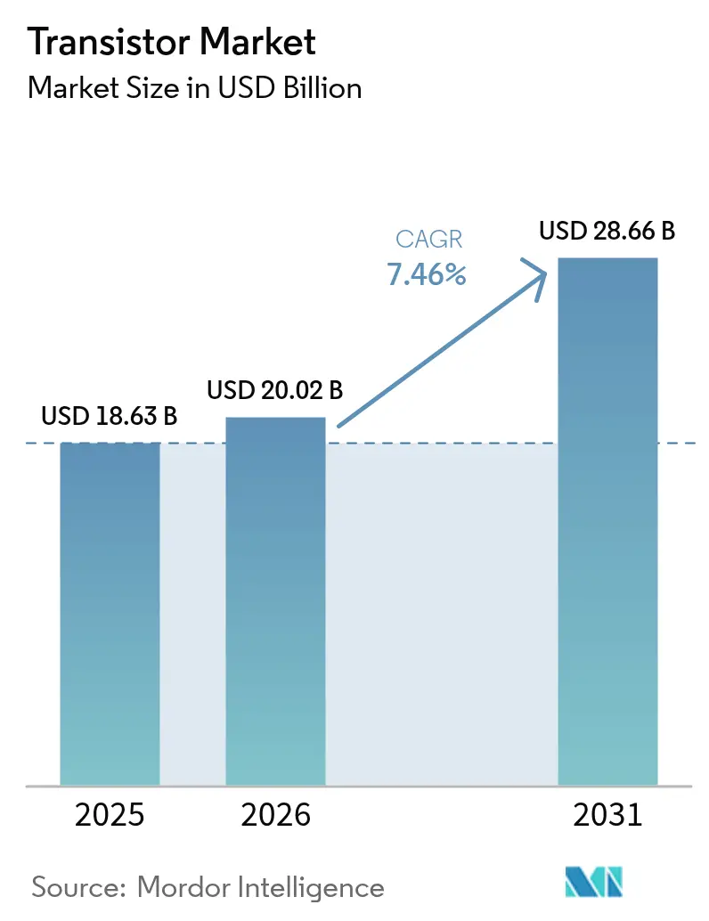
| Market Size (2026) | USD 20.02 Billion |
| Market Size (2031) | USD 28.66 Billion |
| Growth Rate (2026 - 2031) | 7.46% CAGR |
| Fastest Growing Market | Asia Pacific |
| Largest Market | Asia Pacific |
| Market Concentration | Medium |
Major Players *Disclaimer: Major Players sorted in no particular order Image © Mordor Intelligence. Reuse requires attribution under CC BY 4.0. | |
Transistor Market Analysis by Mordor Intelligence
The transistor market size in 2026 is estimated at USD 20.02 billion, growing from 2025 value of USD 18.63 billion with 2031 projections showing USD 28.66 billion, growing at 7.46% CAGR over 2026-2031. Momentum stems from migration toward wide-bandgap materials, rising capital expenditure on regional fabs, and accelerating demand in power-hungry applications such as electric vehicles and 5G infrastructure. Silicon continues to supply most unit volumes in 2024 and is slipping as silicon-carbide and gallium-nitride devices capture sockets that demand higher voltage tolerance and superior thermal conductivity. Asia-Pacific accounted for 56.30% revenue in 2024, aided by China’s localization programs and India’s incentive-backed manufacturing surge. Parallel moves by U.S. and European governments to reshore critical nodes are lifting tool orders, sustaining back-end capacity additions, and widening supply options in the transistor market. Export-control regimes that restrict sub-14 nm processes and high-bandwidth memory have segmented the competitive field, reinforcing the strategic value of domestic fabs and favoring suppliers that control both front-end and packaging assets.
Key Report Takeaways
- By transistor type, bipolar-junction transistors led with 48.35% revenue share in 2025; insulated-gate bipolar transistors are projected to expand at 8.66% CAGR through 2031.
- By material, silicon retained 68.85% of the transistor market share in 2025, while silicon-carbide is forecast to post the fastest 8.86% CAGR between 2026 and 2031.
- By technology node, processes below 10 nm accounted for 10.22% CAGR from 2026 to 2031, whereas ≥65 nm nodes represented 34.25% of the transistor market size in 2025.
- By packaging type, surface-mount held 46.05% of the transistor market size in 2025; wafer-level packaging is advancing at a 9.82% CAGR through 2031.
- By end-user, consumer electronics captured 36.55% of revenue in 2025, while automotive and transportation are growing at a 9.45% CAGR to 2031.
- By region, Asia-Pacific led with 55.90% revenue share in 2025 and is expected to grow fastest with 10.62% CAGR through 2031.
Note: Market size and forecast figures in this report are generated using Mordor Intelligence’s proprietary estimation framework, updated with the latest available data and insights as of 2026.
Global Transistor Market Trends and Insights
Drivers Impact Analysis*
| Driver | (~) % Impact on CAGR Forecast | Geographic Relevance | Impact Timeline |
|---|---|---|---|
| Surging demand for power-efficient mobile SoCs | +1.80% | Global, with APAC leadership | Short term (≤ 2 years) |
| Rapid electrification of transportation and charging infrastructure | +2.10% | North America & EU, expanding to APAC | Medium term (2-4 years) |
| AI/ML inference at the edge driving discrete power devices | +1.50% | Global, concentrated in data center regions | Medium term (2-4 years) |
| 5G-to-6G RF front-end upgrades | +1.20% | Global, led by developed markets | Long term (≥ 4 years) |
| Government incentives for wide-band-gap fabs (SiC, GaN) | +0.70% | North America, EU, select APAC countries | Long term (≥ 4 years) |
| Adoption of advanced packaging (chip-let, 3D stacking) | +0.90% | Global, concentrated in advanced foundries | Medium term (2-4 years) |
| Source: Mordor Intelligence | |||
Surging Demand for Power-Efficient Mobile SoCs
Mobile system-on-chip suppliers are lengthening transistor counts to integrate AI accelerators that execute on-device inference tasks without draining batteries. Chip architectures blend high-performance logic with analog blocks optimized for standby below 10 mW, shifting purchasing criteria from unit price to joules-per-operation. TSMC’s 3 nm production lines entered mass production during 2025 mainly to serve smartphone SoCs, underscoring how node migration remains anchored in mobility workloads.[1]Tokyo Electron Ltd., “Announcement of New Production Building Construction in Miyagi,” tel.com Heterogeneous integration is reinforcing wafer-level packaging adoption as designers co-locate neural-processing cores and power-management circuitry on a single substrate. Although global smartphone shipments plateaued, rising silicon per handset is sustaining revenue growth across the transistor market.
Rapid Electrification of Transportation and Charging Infrastructure
Electric vehicles embed roughly 10 times more semiconductors than combustion models, most of which are high-current transistors handling traction inverters, on-board chargers, and DC-DC converters. The industry shift from 400 V to 800 V systems exceeds the safe-operating area of silicon devices, prompting automakers to specify SiC MOSFETs and IGBT modules rated at 1,200 V. Toshiba’s new 300 mm facility aims to triple automotive-grade power semiconductor output, illustrating supplier responses to this long-cycle opportunity.[2]Silicon.co.uk, “Toshiba Completes New 300-Millimeter Wafer Fabrication Facility for Power Semiconductors,” silicon.co.uk Public fast-charger rollouts add further upside, as each station integrates multiple IGBT stacks and gate drivers. Qualification to AEC-Q100 extends design cycles by up to two years, creating a persistent gap between demand visibility and supply availability that underpins healthy pricing.
AI/ML Inference at the Edge Driving Discrete Power Devices
Edge AI devices, from factory sensors to smart cameras, prioritize energy-efficient inference. Designers, therefore, select transistor architectures capable of low-precision arithmetic and dynamic voltage scaling. Discrete power transistors orchestrate voltage rails that modulate between burst computation and deep sleep, mandating low leakage and instant wake-up characteristics. Research from the Institute for Basic Science showed epitaxial methods that shrink MoS₂ channel widths below 4 nm, revealing future paths to sustain edge performance scaling. Regulatory pushes for greener AI systems, such as Europe’s AI Act, reinforce demand for high-efficiency transistors that aid compliance certifications across industrial markets.
5G-to-6G RF Front-End Upgrades
The leap from 5G to prospective 6G raises peak carrier frequencies into the millimeter-wave and terahertz ranges, driving adoption of GaN-based power amplifiers and switches. Massive-MIMO base-station antennas multiply RF transistor counts per sector, while beam-forming algorithms require ultra-linear gain blocks to preserve signal integrity. Research consortia have already demonstrated terahertz prototypes proving the limits of silicon and reinforcing the case for wide-bandgap alternatives.[3]ChipEstimate.com, “SemiSouth Labs Announces First Use of its Breakthrough Transistor,” chipestimate.com Telecom operators upgrading macro sites to 64T64R configurations could lift overall unit demand even if cell-site growth moderates, sustaining a high-volume replacement cycle through the end of the decade.
Restraints Impact Analysis*
| Restraint | (~) % Impact on CAGR Forecast | Geographic Relevance | Impact Timeline |
|---|---|---|---|
| Quantum-tunnelling limits below 3 nm nodes | -1.20% | Global, concentrated in leading-edge fabs | Long term (≥ 4 years) |
| Supply-chain concentration in Taiwan and South-China | -0.80% | Global, with acute impact on advanced nodes | Short term (≤ 2 years) |
| Rising fab construction CAPEX amid talent shortages | -0.60% | Global, most severe in North America & EU | Medium term (2-4 years) |
| High qualification cost for automotive-grade devices | -0.40% | Global, concentrated in automotive hubs | Medium term (2-4 years) |
| Source: Mordor Intelligence | |||
Quantum-Tunneling Limits Below 3 nm Nodes
Sub-3 nm geometries experience prohibitive leakage due to quantum tunneling, eroding the energy-delay benefit that historically justified node shrinks. Gate-all-around nanosheet transistors partially mitigate electrostatic loss yet demand intricate patterning sequences and expensive EUV multi-patterning steps. Foundries are therefore combining modest gate-length reductions with system-level innovations such as 3D stacking and chiplets to extend performance roadmaps rather than chasing pure lithographic scaling. The cost of a single sub-3 nm mask set now exceeds USD 10 million, meaning only the highest-volume consumer and cloud processors can amortize tooling expenses.
Supply-Chain Concentration in Taiwan and South China
Roughly 62% of global foundry capacity sits in Taiwan, with South China accounting for most back-end assembly lines. Natural-disaster risk, rising cross-strait tensions, and export-license uncertainty elevate lead-time volatility and prompt buffer-stock strategies across automotive and aerospace buyers. The U.S. CHIPS Act and similar EU incentives are steering multi-billion-dollar fab announcements in Arizona, Texas, and Dresden, but those greenfield sites will not reach mature yields until late in the decade.[4]U.S. Government Accountability Office, “Export Controls: Commerce Implemented Advanced Semiconductor Rules and Took Steps to Address Compliance Challenges,” gao.gov Until then, any disruption at coastal Taiwanese fabs or South-Chinese OSATs could reduce quarterly transistor market shipments by double-digit percentages.
*Our forecasts treat driver/restraint impacts as directional, not additive. The impact forecasts reflect baseline growth, mix effects, and variable interactions.
Segment Analysis
By Transistor Type: IGBT Momentum Meets BJT Scale
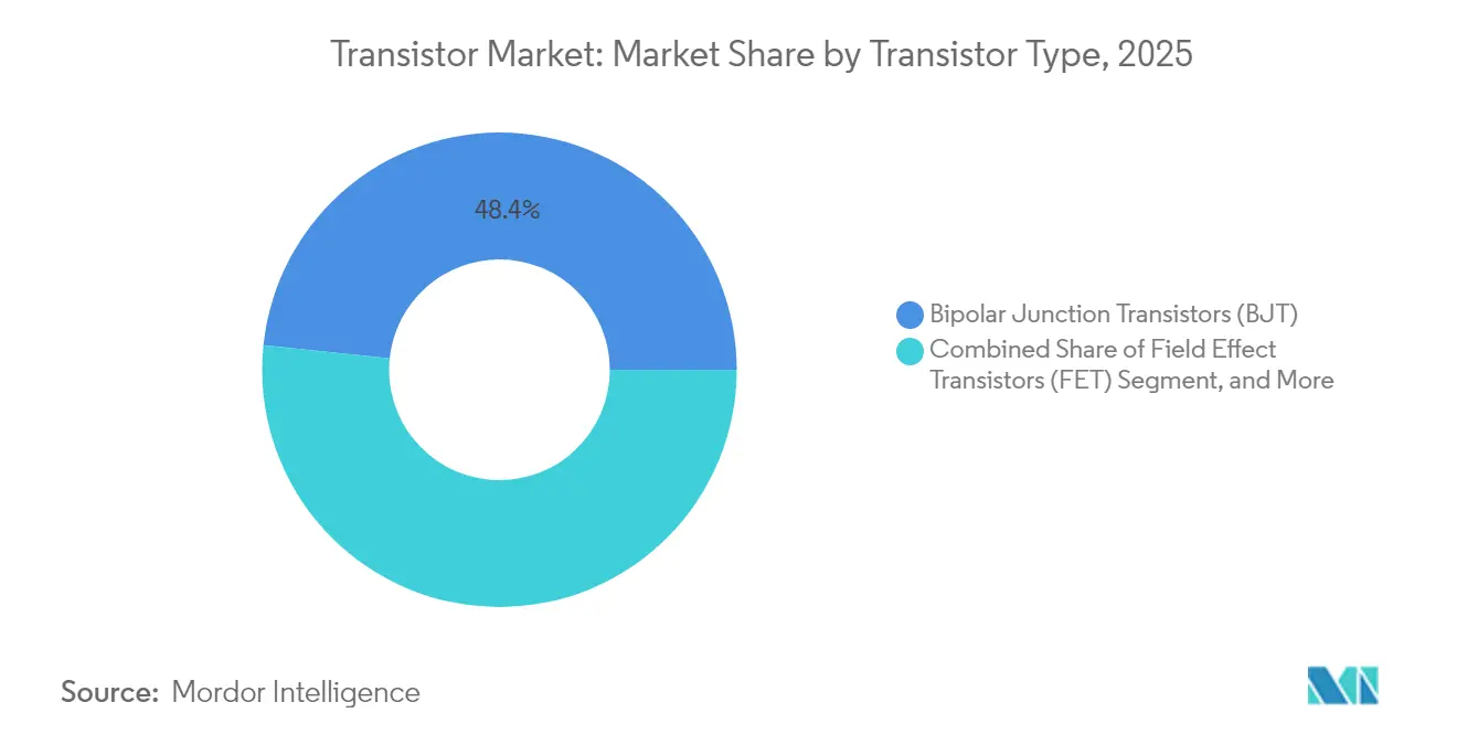
Global IGBT revenue is projected to advance at 8.66% CAGR between 2026 and 2031, outpacing overall transistor market growth as e-mobility and renewable inverters demand high-efficiency switching components. The legacy BJT category retained 48.35% share of the transistor market size in 2025 by serving cost-sensitive consumer and industrial designs that do not need fast switching or extreme voltage tolerance. Suppliers are leveraging wafer-level packages to drive IGBT current ratings beyond 1,000 A while keeping switching loss at competitive levels.
Automotive safety standards, including ISO 26262, elevate barriers to entry by mandating extended mission-profile testing, a factor that supports premium pricing and reinforces moderate industry concentration. Nexperia’s USD 200 million expansion into GaN and SiC processes aligns with customer roadmaps seeking alternative materials that can surpass the ruggedness limits of silicon IGBT structures. Field-effect transistors remain indispensable in logic applications, but their share gains are modest as node scaling slows and discrete counts plateau in smartphones and PCs.


By Material: Wide-Bandgap Uptake Accelerates
Silicon kept 68.85% of the 2025 transistor market share, yet silicon-carbide devices are forecast to log the highest 8.86% CAGR to 2031 as traction inverters, solar inverters, and industrial drives transition to 1,200 V designs that reward lower switching loss. Gallium-nitride’s niche in RF and fast-charger power stages is expanding, although substrate cost and wafer yield remain hurdles to mass penetration.
Government incentives, such as dedicated CHIPS Act grants for SiC pilot lines, ease upfront costs for domestic fabs and shorten the payback period on crystal-growth investments. Still, wide-bandgap wafer yields trail silicon by 20-30 percentage points, inflating die cost and confining adoption to applications where performance benefits justify premiums. Lab demonstrations of SiC JFET audio amplifiers highlight the broadening scope beyond power conversion, signaling future diversification paths for wide-bandgap suppliers.
By Technology Node: Premium Nodes Command Value
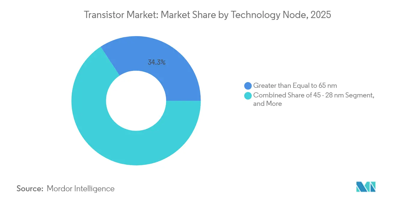
Processes finer than 10 nm capture the highest 10.22% CAGR as handset and data-center processors chase maximum performance per watt, while ≥65 nm nodes retained 34.25% of the transistor market size in 2025 thanks to robust demand for power management ICs and microcontrollers. Mask set cost for sub-7 nm production obliges design win volumes in the hundreds of millions to justify tape-out, steering many industrial and automotive ICs toward 28-40 nm, where tooling fees are manageable and mature yield curves sustain profit.
Tokyo Electron’s decision to invest USD 104 billion in advanced etch and deposition capacity reflects confidence that leading-edge nodes will retain pricing power even as Moore’s Law improvements flatten. Adoption of extreme ultraviolet lithography supports pattern fidelity but intensifies the capital barrier, concentrating leading-edge supply among two foundries whose combined output still lags demand.
By Packaging Type: System-in-Package Gains Traction
Surface-mount packages held a 46.05% share in 2025 because they fulfill mainstream cost, reliability, and board-space constraints across consumer and industrial goods. Wafer-level packaging is forecast to log a 9.82% CAGR, enabling chiplets, fan-out die redistribution, and high-bandwidth memory integration within footprints suited for mobile devices. Through-hole packages linger in avionics and utility-scale power applications where mechanical robustness and thermal mass trump miniaturization.
CoWoS and similar 2.5D technologies join logic dies with stacked HBM, reaching bandwidths beyond 1 TB/s required by training-class AI accelerators. Such densities push package thermal load above 100 W/cm², compelling adoption of copper micro-vias, vapor-chamber lids, and direct-fluid cooling. Sourcing of ultra-flat organic substrates has emerged as a hidden constraint, nudging OSATs toward vertical integration with laminate suppliers.
By End-User Industry: Transportation Propels New Demand
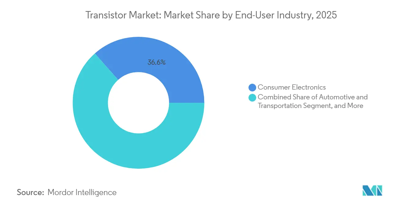
Consumer electronics comprised 36.55% of 2025 revenue, yet growth moderates along with handset and television replacement cycles. Automotive and transportation segments will post the highest 9.45% CAGR through 2031, lifted by full-hybrid, battery-electric, and fuel-cell drivetrains that multiply power-device counts per vehicle.
Information and communication technology continues to absorb high-frequency RF transistors for 5G base stations and soon-to-arrive 6G prototypes. Energy and power segments rely on high-voltage SiC modules in photovoltaic string inverters and utility-grade storage, while aerospace and defense customers demand radiation-hardened parts that survive ionizing environments. Healthcare’s shift to wearables and implantables favors sub-threshold transistors that function on harvested energy, opening a specialized but promising avenue for low-leakage device makers.
Geography Analysis
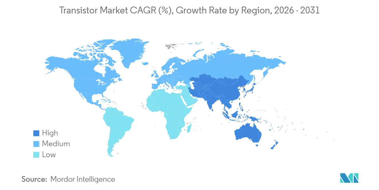
Asia-Pacific contributed 55.90% revenue in 2025 and is forecast to record a 10.62% CAGR to 2031. China’s domestic foundries are scaling 28 nm and 14 nm lines under policy mandates, yet leading-edge constraints drive procurement from Taiwanese and South Korean fabs. India’s production-linked incentive program has attracted multiple OSAT announcements, but logistics and skilled-labor gaps still temper near-term output. Japan maintains a critical role in photoresist, silicon-wafer, and deposition-tool supply, cushioning its transistor market relevance despite limited wafer-fab capacity. Emerging Southeast-Asian hubs such as Vietnam and Malaysia gain as second-source alternatives when multinationals diversify away from coastal China.
North America benefits from cloud-data-center expansion, electric-vehicle assembly growth, and defense-program mandates that prioritize domestic sourcing. The CHIPS Act’s USD 52 billion allocation has unlocked multi-fab investments by TSMC, Samsung, and Intel, improving long-term supply security. Canada’s focus on 5G infrastructure and battery-electric buses spurs specialized demand for RF and high-power devices, while Mexico’s EMS clusters near the U.S. border attract transistor assembly lines that service automotive Tier-1 suppliers. Regional policy emphasis on supply-chain resilience supports a price premium that partially offsets elevated labor and construction costs.
Europe’s transistor market gravitates around Germany’s e-mobility shift, France’s aerospace sector and the region-wide Green Deal that penalizes inefficient power conversion. Germany’s OEMs are solo-sourcing SiC devices to stabilize inverter roadmaps, while French defense programs specify radiation-hardened transistors that endure harsh cosmic-ray environments. The European Chips Joint Undertaking funds advanced-node pilot lines with a dual objective: strategic autonomy and measurable carbon-footprint reduction. Brexit-related trade frictions prompt British OEMs to dual-source assemblies from continental OSATs, creating share opportunities for local suppliers in the Benelux corridor.

Regulatory Landscape
Trade and procurement controls increasingly shape cross-border supply for transistors and related semiconductor products. In the United States, Proclamation 11002 invoked Section 232 and set a 25% ad valorem tariff on a narrow category of advanced logic semiconductors effective January 15, 2026, alongside a broader national-security framing for semiconductor and equipment imports. This approach affects sourcing, documentation, and investment planning across global supply chains.
In Europe, product-sustainability and interoperability rules are tightening around downstream electronics that influence transistor demand and design choices. Commission Regulation (EU) 2025/2052 (adopted October 13, 2025) updates ecodesign requirements for external power supplies and related charging equipment, while common charger requirements extend to laptops from April 28, 2026 and the repair-of-goods directive applies from July 31, 2026. Together, these measures encourage longer-life devices and more standardized power interfaces.
Value Chain Analysis
The transistor value chain covers upstream raw materials and specialty inputs (silicon wafers, SiC substrates, specialty gases and chemicals), semiconductor manufacturing equipment, and front-end wafer fabrication by both IDMs and foundries across leading-edge and mature nodes. It then moves to back-end assembly, test, and advanced packaging via OSATs, before distribution to OEMs and EMS providers across consumer electronics, automotive, industrial, ICT, and energy markets. OECD mapping points to deep geographic specialization, with material and tool ecosystems concentrated in East Asia, while assembly and packaging capacity is expanding into the United States and Southeast Asia as companies diversify footprints.
Bottlenecks are most acute in low-redundancy upstream inputs (precision substrates and specialty chemicals) and in access to leading-edge capacity. These constraints can limit transistor supply for high-performance logic, while also competing for equipment and skilled labor needed for power and analog lines. Policy-driven localization and capital programs are reshaping the chain, including large new U.S. fab commitments such as TSMC’s July 2026 incremental USD 100 billion Arizona expansion announcement. At the same time, export controls on critical minerals and materials, including China’s April 2025 regime covering rare earths such as yttrium and scandium per the cited summaries, reinforce multi-sourcing and qualification of alternative suppliers across the ecosystem.
Competitive Landscape
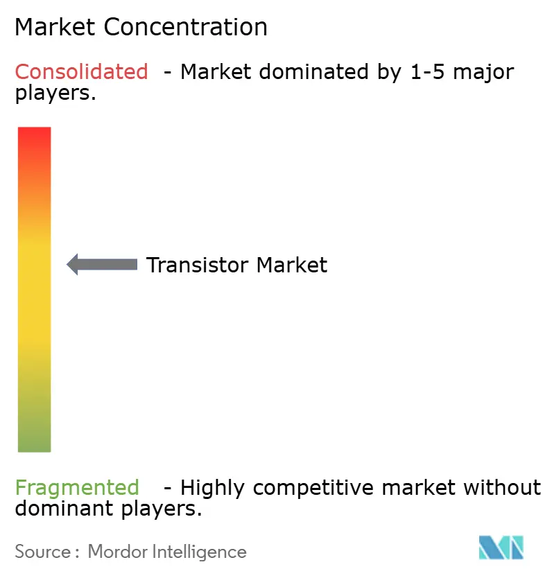
Global revenue is moderately concentrated, with the top five suppliers controlling roughly a major part of the sales. Infineon leverages a cradle-to-grave product stack that spans discrete power devices, dedicated driver ICs, and advanced modules mounted on direct-bonded copper substrates. STMicroelectronics integrates silicon and SiC production inside its European fabs, aligning with automotive OEMs that seek one-stop sourcing for traction inverters and on-board chargers. Texas Instruments dominates high-volume analog and logic products that depend on reliable 300 mm trailing-edge wafers and large sales coverage teams.
Capital intensity has climbed as advanced tools and EUV cranes raise greenfield fab outlays above USD 20 billion. Consequently, newcomers gravitate toward fab-light models, focusing on design IP, vertical application know-how, and selective capacity reservation at foundries. Patent cross-licensing is expanding, with recent deals among wide-bandgap specialists aimed at covering trench designs, gate oxides, and thermal interface methods. White-space opportunities persist in quantum computing control ICs, where conventional CMOS struggles with cryogenic noise targets, and in mm-wave RF devices exceeding 90 GHz, where GaN on SiC leads performance benchmarks.
Export control regimes introduced since 2024 favor companies that already possess dual-or-multi-region production footprints. Suppliers concentrated in one geography face qualification challenges when customers demand second source guarantees free from licensing delays. Vertical integration into advanced packaging further distinguishes leaders, allowing them to co-optimize die, interposer and thermal spreader design. This capability has proven critical for AI accelerator customers that cannot tolerate yield drag or signal-integrity loss inside 3D-stacked modules.
Transistor Industry Leaders
Diodes Incorporated
Infineon Technologies AG
ROHM Co., Ltd.
NXP Semiconductors N.V.
Vishay Intertechnology, Inc.
- *Disclaimer: Major Players sorted in no particular order

Market Opportunities and Future Outlook
Wide-bandgap power devices and packaging-intensive architectures are the clearest whitespace areas where performance requirements and supply constraints intersect. Automotive electrification and charging infrastructure continue to pull SiC MOSFETs and IGBT modules into higher-voltage designs, including 800 V platforms. Data centers and telecom infrastructure also intensify demand for efficient power conversion and high-frequency switching, which creates room for suppliers that can deliver qualified device-plus-package solutions rather than shipping discrete die alone.
On the advanced-node side, the shift from FinFET to gate-all-around (GAA) nanosheet transistors creates opportunities across equipment, materials, and packaging ecosystems that support tighter process windows and higher interconnect density. The 2024 IRDS roadmap work and public foundry roadmaps on GAA highlight ongoing technology migration, while large-scale capacity actions signal where supply is being built. TSMC’s July 2026 announcement to expand U.S. manufacturing with additional Arizona fabs focused on 2 nm and below increases the strategic value of localized supply chains for transistors used in high-performance compute, RF front ends, and power management. These capacity moves also raise demand for specialty etch, deposition, and advanced packaging capabilities used in nanosheet stacks and heterogeneous integration.
Recent Industry Developments
- July 2026: Diodes Incorporated announced a definitive agreement to acquire ElevATE Semiconductor for USD 250 million to broaden its analog and mixed-signal portfolio serving automated test equipment applications. The deal adds design capability and customer access in a niche tied to transistor characterization and production test, supporting pull-through for related discretes and analog components.
- July 2026: Infineon Technologies AG opened its Smart Power Fab in Dresden after a EUR 5 billion investment, expanding local manufacturing capacity for intelligent power semiconductors and analog/mixed-signal technologies. The added capacity strengthens European supply for power and control devices used in automotive, industrial drives, and energy applications, where qualification cycles and supply assurance influence sourcing decisions.
- May 2026: Infineon Technologies AG said the U.S. International Trade Commission ruled in its favor in a GaN-related patent case against Innoscience and ordered import and sales bans for infringing products. The decision tightened competitive access to the U.S. market for certain GaN device offerings, reinforcing the role of IP enforcement in shaping supplier options for wide-bandgap transistor adoption.


Research Methodology Framework and Report Scope
Market Definition and Coverage
This market covers the global revenue generated from transistors supplied as electronic components across major end-use industries. The value is counted at the point of sale from device makers to customers through direct and distribution channels.
Scope exclusions: We exclude foundry services revenue, design IP licensing, and finished electronic products where the transistor value is already embedded in a higher-level system price.
Segmentation Overview
- By Transistor Type
- Bipolar Junction Transistors (BJT)
- Field Effect Transistors (FET)
- Insulated Gate Bipolar Transistors (IGBT)
- Heterojunction Bipolar Transistors (HBT)
- By Material
- Silicon (Si)
- Silicon Carbide (SiC)
- Gallium Nitride (GaN)
- Germanium (Ge)
- By Technology Node
- Greater than Equal to 65 nm
- 45 - 28 nm
- 22 - 16 nm
- 14 - 10 nm
- Less than 10 nm
- By Packaging Type
- Through-Hole
- Surface-Mount
- Chip-Scale Package (CSP)
- Wafer-Level Package (WLP)
- By End-User Industry
- Consumer Electronics
- Information and Communication Technology
- Automotive and Transportation
- Industrial Manufacturing
- Energy and Power
- Aerospace and Defense
- Healthcare and Medical Devices
- By Geography
- North America
- United States
- Canada
- Mexico
- South America
- Brazil
- Argentina
- Colombia
- Rest of South America
- Europe
- United Kingdom
- Germany
- France
- Italy
- Spain
- Rest of Europe
- Asia-Pacific
- China
- Japan
- South Korea
- India
- Rest of Asia-Pacific
- Middle East and Africa
- Middle East
- Saudi Arabia
- United Arab Emirates
- Rest of Middle East
- Africa
- South Africa
- Egypt
- Rest of Africa
- Middle East
- North America
Data Sources, Market Sizing, and Validation
Desk Research
Desk research started with building a clean view of the transistor supply chain, from wafer processing and device manufacturing through packaging, distribution, and end markets. We relied on public sources such as WSTS semiconductor statistics, Semiconductor Industry Association factbooks, UN Comtrade trade flows, OECD industrial indicators, and IEEE and other peer-reviewed electronics journals to ground assumptions around demand cycles and technology shifts.
To translate industry activity into market value, we also reviewed company annual reports, 10-K style filings, investor presentations, and official press releases that discuss capacity additions, product mix, and pricing commentary. In parallel, patent databases were used to track innovation intensity by device type and material (for example silicon versus SiC and GaN), which helped validate which parts of the market were gaining share. We also used paid subscriptions for company financials and intelligence, news and financials, and patent databases to cross-check timelines and normalize disclosures. The desk sources listed here are illustrative, and additional public datasets and documents were used for data collection, validation, and clarification.
Primary Interviews and Surveys
Primary work focused on interviews and short surveys with component suppliers, distributors, and device buyers serving end markets such as consumer electronics, communications, automotive, industrial, and energy applications. We used these discussions to confirm what was shipping in volume, how pricing was moving for key device families, and where demand was being constrained by qualification cycles, lead times, or substitution to adjacent devices. Because this is a global market, inputs were balanced across APAC, EMEA, and the Americas so regional mix and currency timing could be checked with people closest to local demand signals.
Distribution of primary research fieldwork respondents
| Company type | Respondent position | Region |
|---|---|---|
| Top tier: 30% | CXOs: 13% | APAC: 49% |
| Mid tier: 55% | Functional/Unit leaders: 42% | EMEA: 32% |
| Smaller Players: 15% | Managers: 45% | Americas: 19% |
Market-Sizing & Forecasting
Sizing was built using a top-down and bottom-up approach, where semiconductor demand signals and device mix are first reconstructed from end-use production activity and trade indicators, then validated through sampled pricing and volume checks. On the top-down side, we linked transistor consumption to practical drivers such as electronics unit production, vehicle electrification content, 5G and data-center infrastructure rollouts, and industrial power conversion demand, so the total ties back to real shipment pull.
These totals were then corroborated with selective bottom-up approximations, such as rolling up revenue ranges from disclosed company segments, applying ASP-by-device-family checks (for example small-signal versus power devices), and channel feedback on allocation and inventory correction patterns. Key model inputs included the mix shift toward SiC and GaN in power applications, packaging transitions (through-hole versus surface-mount and advanced packages), technology node migration for high-volume devices, regional manufacturing concentration in APAC, and typical pricing behavior during upcycles and digestion periods. For forecasting, scenario analysis was used to reflect demand uncertainty, and assumptions on EV build rates, industrial capex, and network spending were reviewed with industry respondents before finalizing growth paths. Where bottom-up inputs had gaps, conservative interpolation was applied and then stress-tested through follow-up calls and cross-checks against independent demand indicators.
Data Validation & Update Cycle
Before sign-off, we run multiple checks so the final market values are consistent with external signals and with internal logic across regions and end uses. Model outputs are compared with independent indicators such as semiconductor cycle commentary, trade flows for relevant device categories, and reported capacity changes. If any large variance appears, it is investigated until a clear reason is documented.
Anomaly checks are followed by a multi-step analyst review, where assumptions, unit conversions, and currency timing are re-verified. Outlier growth rates are also challenged using alternate data cuts. If primary inputs conflict with desk findings, respondents are re-contacted to clarify definitions or to update recent pricing and mix changes. Reports are refreshed annually, with interim updates when material events occur, and a final pre-delivery review is completed so clients receive the most current view.
Mordor Intelligence's Global Transistor Market Sizing Compared With Other Published Estimates
Published market sizes for transistors often do not match because the underlying scope and counting method differ, even when the headline name looks the same. The biggest swings usually come from whether the estimate is counting only discrete transistors or also including adjacent power modules, integrated components, or broader semiconductor device groupings.
The main gap comes from silicon-only versus all-material coverage and from what gets counted as a transistor sale. Mordor Intelligence counts discrete transistor value across silicon, SiC, and GaN while keeping foundry services and higher-level system revenue out of the total. Differences also show up when one estimate uses an aggressive price ramp for wide-bandgap devices, or when currency conversion is taken from a different point in the year. Finally, refresh cadence matters because inventory correction cycles can change near-term values quickly, and older snapshots may miss recent pricing normalization or demand recovery.
Benchmark comparison
| Source | Market Size | Gaps in Research Methodology |
|---|---|---|
| Mordor Intelligence | USD 20.02 B (2026) | |
| Industry Publisher A | USD 18.72 B (2025) | Uses a different base year and appears to apply a broader qualitative definition that can blend discrete and integrated contexts, which can shift what is counted as market revenue. |
| Industry Publisher B | USD 24.40 B (2024) | Limits the scope to silicon transistors only and does not clearly separate discrete device value from adjacent electronics content, which can inflate the comparable total versus an all-material discrete definition. |
Looking across the figures, the spread is largely explained by scope choices (silicon-only versus all materials) and by whether the counting stays at the component revenue level. By keeping assumptions tied to observable demand drivers and by validating pricing and mix with primary inputs, the resulting market size remains traceable to repeatable steps that users can sanity-check.


Key Questions Answered in the Report
What is the forecast value of the global transistor market by 2031?
The transistor market is projected to reach USD 28.66 billion by 2031.
Which material segment is growing the fastest?
Silicon-carbide devices are expected to post the highest 8.86% CAGR between 2026 and 2031.
Why are insulated-gate bipolar transistors gaining traction?
IGBTs combine MOSFET switching speed with bipolar conduction efficiency, making them ideal for 800 V electric-vehicle drivetrains.
How will government incentives affect regional supply?
Programs such as the U.S. CHIPS Act and EU pilot lines are funding new fabs that diversify supply away from East Asia.
Which packaging technology has the strongest growth outlook?
Wafer-level packaging is forecast to grow at a 9.82% CAGR thanks to chiplet and 3D-stacking adoption.
What is the main restraint to continued node scaling?
Quantum-tunneling leakage below 3 nm limits further voltage scaling and raises leakage, curbing the benefits of smaller geometries.
Page last updated on: