Substrate Market Size and Share
Market Overview
| Study Period | 2020 - 2031 |
|---|---|
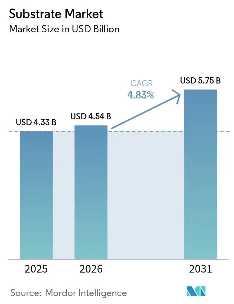
| Market Size (2026) | USD 4.54 Billion |
| Market Size (2031) | USD 5.75 Billion |
| Growth Rate (2026 - 2031) | 4.83% CAGR |
| Fastest Growing Market | Asia-Pacific |
| Largest Market | Asia-Pacific |
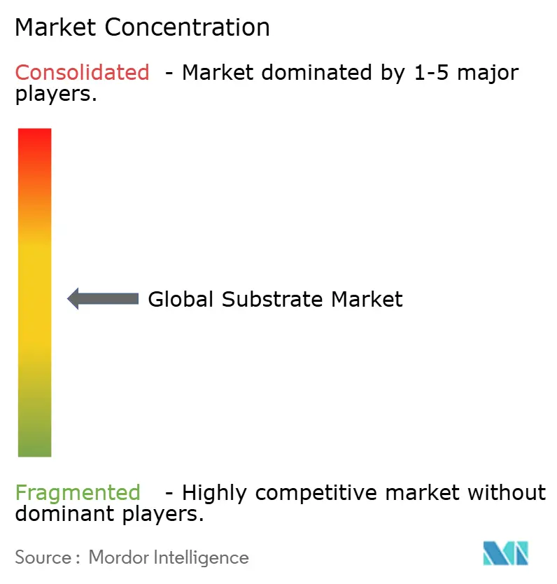
| Market Concentration | Medium |
Major Players *Disclaimer: Major Players sorted in no particular order Image © Mordor Intelligence. Reuse requires attribution under CC BY 4.0. | |
Substrate Market Analysis by Mordor Intelligence
The substrate market size was valued at USD 4.33 billion in 2025 and estimated to grow from USD 4.54 billion in 2026 to reach USD 5.75 billion by 2031, at a CAGR of 4.83% during the forecast period (2026-2031). Demand is rising as AI accelerator architectures, 5G radio deployments, and electric-vehicle (EV) power-electronics broaden the application base for advanced packaging laminates. Expansion is moderate because traditional printed-circuit infrastructure is mature, yet design wins linked to heterogeneous integration are raising average substrate value per device. Competitive intensity is shaped by supply-chain exposure to high-Tg resins, the capital burden tied to new fabrication lines, and sustainability mandates curbing halogenated laminates. Asia Pacific keeps a leadership edge thanks to clustered semiconductor assembly operations, swift capacity additions in Taiwan, South Korea, and China, and regional policy support that lowers production costs.
Key Report Takeaways
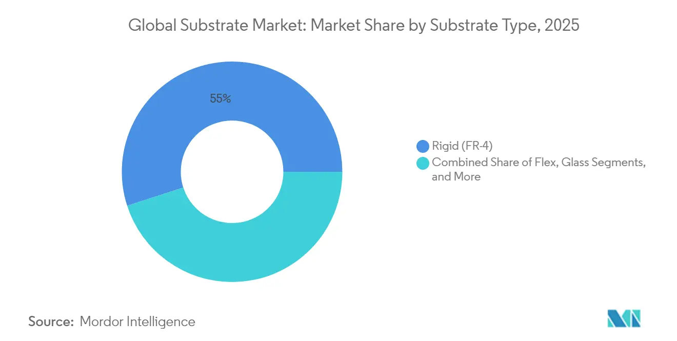
- By substrate type, rigid FR-4 captured a 54.98% share of the substrate market in 2025, while glass substrates are set to grow the quickest at a 5.54% CAGR through 2031.
- By material, FR-4 epoxy glass held 41.88% of the substrate market size in 2025; glass materials record the fastest 5.42% CAGR to 2031.
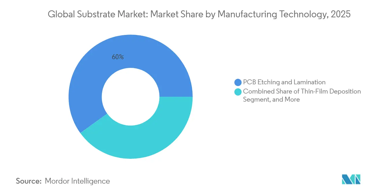
- By manufacturing technology, PCB etching and lamination represented 59.95% of the substrate market share in 2025, whereas fan-out wafer-level packaging is projected to expand at a 5.62% CAGR.
- By end-user industry, computing and data storage accounted for 29.22% of the substrate market in 2025, yet automotive and transportation is advancing at a 5.12% CAGR.
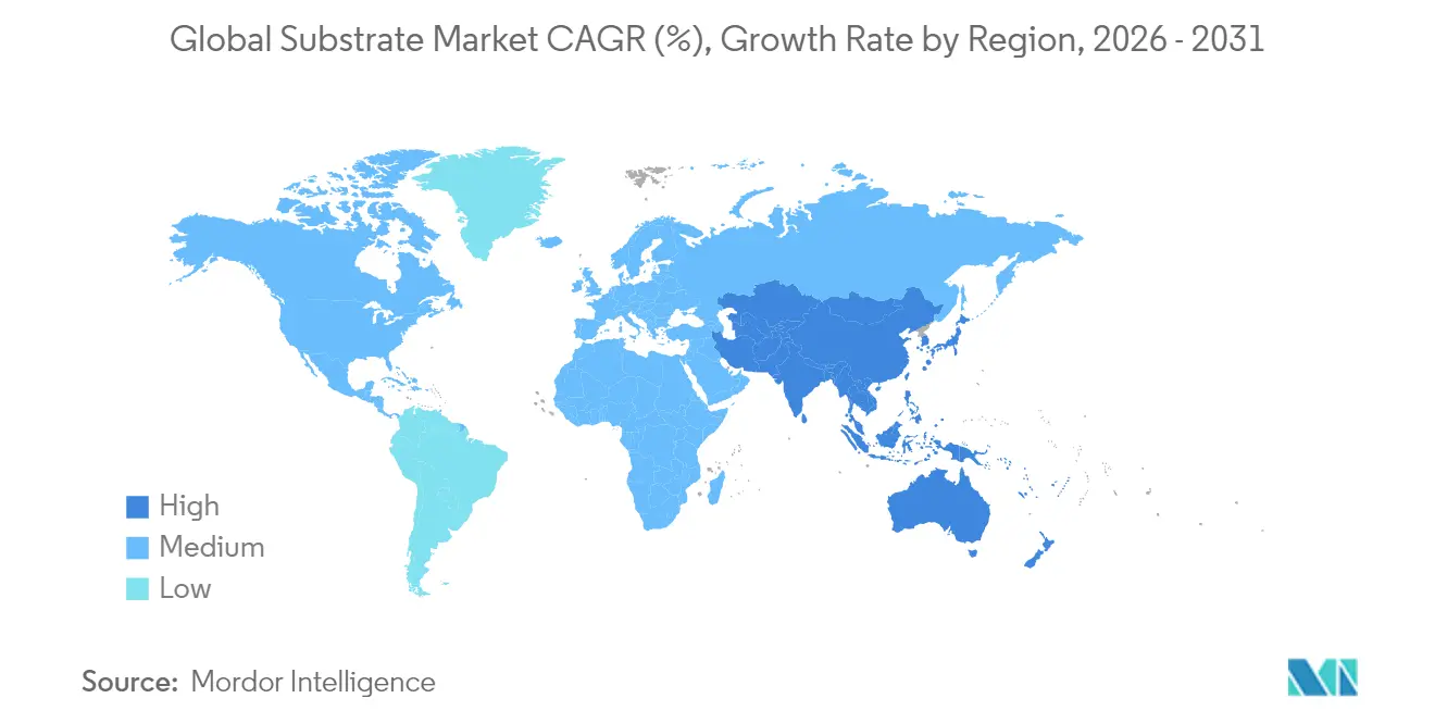
- By geography, Asia Pacific commanded a 37.92% share in 2025 and continues as the fastest-growing region with a 5.29% CAGR to 2031.
Note: Market size and forecast figures in this report are generated using Mordor Intelligence’s proprietary estimation framework, updated with the latest available data and insights as of 2026.
Global Substrate Market Trends and Insights
Drivers Impact Analysis*
| Driver | (~) % Impact on CAGR Forecast | Geographic Relevance | Impact Timeline |
|---|---|---|---|
| Proliferation of heterogeneous integration in AI accelerators | +1.2% | Global, with concentration in APAC and North America | Medium term (2-4 years) |
| Miniaturization demand in mobile and wearable devices | +0.8% | Global, led by APAC manufacturing hubs | Short term (≤ 2 years) |
| 5G roll-outs boosting high-frequency RF substrates | +0.9% | North America, Europe, APAC core markets | Medium term (2-4 years) |
| EV power-electronics adoption of ceramic and metal-core substrates | +0.7% | Global, with early gains in Europe, China, North America | Long term (≥ 4 years) |
| Emergence of chiplet-based packages | +1.0% | APAC core, spill-over to North America | Medium term (2-4 years) |
| Regional semiconductor subsidy races | +0.6% | North America, Europe, select APAC regions | Long term (≥ 4 years) |
| Source: Mordor Intelligence | |||
Proliferation of Heterogeneous Integration in AI Accelerators
Heterogeneous integration allows multiple specialized dies to work together inside a single package, raising substrate complexity requirements. Intel targets 10 × higher interconnect density over organic laminates using glass substrates, enabling logic, memory, and accelerator chiplets to coexist without signal-integrity losses.[1]Intel Corporation, “Glass Substrate Technology Roadmap,” newsroom.intel.com Organic FR-4 cannot match these routings at fine pitches, which encourages designers to transition toward glass, advanced organic, and ceramic options. Package architectures now mix high-speed interfaces next to sensitive analog rails, so dielectric loss, coefficient of thermal expansion, and via reliability become critical selection criteria. Fabricators invest in higher-resolution lithography and laser drilling to meet line/space rules under 10 µm. As AI workloads continue scaling, packaging-centric performance gains are as important as front-end node shrinks, sustaining premium pricing for advanced substrates.
Miniaturization Demand in Mobile and Wearable Devices
Smartphone boards are shrinking while component counts rise, pressing suppliers to deliver thinner, denser, and more flexible substrate constructions. Rigid-flex designs with polyimide cores help route high-speed buses around fold lines without cracking. Wearables further compress stack-ups, forcing the adoption of embedded passive components inside the core layers. Makers in China, South Korea, and Vietnam doubled orders for flexible laminates after 2024 design cycles, lifting utilization in flex substrate factories. Tighter component clearances heighten heat buildup; hence, metal-core variants with aluminum backing are entering high-end mobile segments. These dynamics keep substrate market revenue expanding even when handset unit volumes plateau because value per board creeps higher.
5G Roll-Outs Boosting High-Frequency RF Substrates
Millimeter-wave base stations operate beyond 28 GHz, demanding ultra-low dielectric loss. Rogers Corporation commercialized PTFE-based laminates with stable Dk and Df across −40 °C to 105 °C, capturing multi-layer antenna array designs.[2]AMD Inc., “Chiplet Architecture and Advanced Packaging,” amd.com OEMs request controlled-impedance stack-ups with copper roughness less than 2 µm to limit insertion loss. Equipment makers simultaneously lower board cost by blending high-frequency cores only where needed, sandwiching them between less costly prepregs. Because 5G densification is staggered by region, substrate suppliers enjoy a multi-year revenue runway as operators phase upgrades. North America and Japan drove initial demand in 2024, while Europe and India scale orders through the forecast window.
EV Power-Electronics Adoption of Ceramic and Metal-Core Substrates
EV inverters and onboard chargers switch at hundreds of kilohertz, creating thermal hotspots that overwhelm standard epoxy-glass. Ceramic substrates using aluminum nitride offer thermal conductivity above 150 W/mK while still isolating high voltages, enabling smaller module footprints. Manufacturers such as Kyocera qualified ceramic boards for automotive reliability grades in 2025 testing cycles, boosting order backlogs for 2026 model launches. In mid-power cases, metal-core substrates with aluminum plates dissipate heat at one-third the cost of full ceramic, supporting a tiered product mix. As global EV sales approach 40 % of new-vehicle volumes in 2030, every power-module supplier requires a thermally enhanced substrate strategy, driving continuous adoption across price bands.
Restraints Impact Analysis*
| Restraint | (~) % Impact on CAGR Forecast | Geographic Relevance | Impact Timeline |
|---|---|---|---|
| Supply-chain volatility for high-Tg resins | -0.8% | Global, with acute impact in APAC manufacturing | Short term (≤ 2 years) |
| CAPEX intensity of advanced substrate lines | -1.1% | Global, concentrated in advanced manufacturing regions | Medium term (2-4 years) |
| Technological lock-in risk for legacy PCB fabs | -0.6% | North America and Europe, with spillover to APAC | Medium term (2-4 years) |
| Sustainability pressure on halogenated laminates | -0.4% | Europe and North America, expanding to global markets | Long term (≥ 4 years) |
| Source: Mordor Intelligence | |||
Supply-Chain Volatility for High-Tg Resins
Only a handful of chemical producers offer resins that survive above 170 °C glass-transition temperatures, so any outage tightens spot supply and spikes pricing. Trade restrictions on epoxy precursors raised lead times to 24 weeks during 2024, forcing substrate vendors to hold larger safety stocks. Inventory carrying costs erode margins, especially for small and mid-size shops. Automotive and aerospace customers mandate high-Tg boards for under-hood and avionics assemblies, so substitution with standard FR-4 is not feasible. Suppliers negotiate long-term contracts yet remain vulnerable to geopolitical disruptions around major resin-manufacturing centers in East Asia.
CAPEX Intensity of Advanced Substrate Lines
A single advanced glass-substrate fab demands over USD 100 million in precision lithography, plasma etch, and metrology tools, yielding depreciation charges that can outstrip operating profits in a down cycle. Smaller PCB firms struggle to finance upgrades while maintaining legacy revenue streams, prompting mergers or facility closures. Equipment lead times exceed 12 months, so capacity cannot be added swiftly once demand surges. The high investment hurdle slows industry response to new design wins, sometimes handing orders to vertically integrated giants that can self-fund expansions. Capital scarcity therefore tempers substrate market growth despite strong end-market pull.
*Our forecasts treat driver/restraint impacts as directional, not additive. The impact forecasts reflect baseline growth, mix effects, and variable interactions.
Segment Analysis
By Substrate Type: Glass Substrates Drive Next-Generation Packaging
Rigid FR-4 retained a 54.98% slice of the substrate market share in 2025, reflecting entrenched infrastructure and low unit costs. The segment addresses mainstream notebooks, televisions, and home appliances that prize cost per square inch over bleeding-edge performance. In contrast, glass substrates record a 5.54% CAGR, the fastest pace across types, because AI accelerators and switch-ASIC roadmaps now mandate up to 10 × interconnect density. That requirement pulls demand toward glass interposers capable of tighter dimensional tolerances and low CTE mismatch. Ceramic substrates occupy a stable niche in power-dense circuits, while metal-core boards pick up LED lighting and mid-power designs. Flex and rigid-flex constructions hold share in foldable phones and automotive infotainment panels where bend radii beat rigid boards. Looking forward, the substrate market size for glass lines is projected to exceed USD 1.07 billion by 2031 as yield learning curves trim per-layer costs. Suppliers split capacity between high-layer glass and cost-optimized FR-4 to hedge cyclical swings.
A growing list of chip vendors adopt glass for reticle-sized interposers, lifting order visibility for specialty panel fabs and sparking partnerships with equipment makers. Pilot production runs delivered defect densities under 50 ppm in 2025, supporting volume ramps from 2026 onward. Yet rigid FR-4 remains relevant for price-sensitive consumer electronics, and its deep supply base provides negotiating leverage to OEMs. Hybrid stack-ups that laminate glass cores inside FR-4 shells emerge as a bridge technology, helping customers transition without wholesale redesigns. Overall, coexistence rather than outright replacement defines the next five-year substrate mix.


By Material: Advanced Materials Challenge FR-4 Dominance
FR-4 epoxy glass held a 41.88% revenue share in 2025 thanks to its balanced mechanical strength, flame retardancy, and low price. Glass materials, however, chart the leading 5.42% CAGR through 2031 by enabling finer line/space and reducing warpage in large substrates. BT resin provides lower dielectric constants suited to high-speed serial links, capturing advanced networking cards. Polyimide layers withstand continuous service up to 260 °C, supporting aerospace and down-hole drilling electronics where FR-4 fails. Ceramic plates of aluminum nitride or alumina reach thermal conductivities above 150 W/mK, making them indispensable in SiC-based EV inverters. Metal-core laminates combine copper or aluminum backers with prepreg, offering an intermediate thermal step that balances cost and performance for LED drivers.
Material innovators tailor filler chemistry to lower loss tangent at mmWave bands, an attribute critical for 5G front-end modules. Sustainability drives demand for halogen-free alternatives compliant with RoHS and REACH, spurring incremental product launches from resin suppliers. As heterogeneous integration tightens line widths, coefficient of thermal expansion convergence between substrate and silicon becomes essential, giving glass an edge at high layer counts. Taken together, the substrate market continues fragmenting by material family as no single option satisfies every performance and cost target.
By Manufacturing Technology: Traditional Methods Face Advanced Packaging Pressure
PCB etching and lamination generated 59.95% of 2025 revenue, underpinned by amortized equipment and widespread engineering knowledge. These subtractive techniques remove copper to delineate traces and press multiple cores into a stack. Yield rates exceed 98% for four-layer consumer products, keeping per-panel costs low. Fan-out wafer-level packaging, though, charts a 5.62% CAGR, propelled by chiplet adoption and the wish to eliminate silicon interposers. Redistribution layers (RDL) in fan-out stacks achieve sub-10 µm wiring and incorporate under-fill molds to support die. Thin-film deposition processes, using sputtering and electroplating, address niche RF multilayers where uniformity across large panels is paramount. Additive manufacturing, such as aerosol jet printing, cuts material waste during prototyping and allows conformal routing on complex shapes.
Embedded-die construction embeds active silicon inside cavities milled into the substrate, slashing parasitic inductance and height profiles. However, reliability testing extends time-to-market, limiting mainstream adoption until automotive-grade qualifications are expected to complete in 2026. In the near term, customers select technology based on cost-per-I/O and electrical performance. Large-volume handset boards will continue running on incremental FR-4 lines, whereas AI accelerators and high-speed network switches move to fan-out or glass panel routes. Therefore, the substrate market size growth hinges on hybrid production setups melding established etching with advanced RDL cells.
By End-User Industry: Automotive Growth Challenges Computing Leadership
Computing and data-storage systems consumed 29.22% of 2025 shipments, reflecting hyperscale data-center builds and enterprise server refresh cycles. Each new CPU socket packs larger interposers and more DDR channels, so server boards add layers and area. Automotive and transportation, however, is forecast to expand at a 5.12% CAGR through 2031, the steepest trajectory among verticals. The pivot to battery-electric drivetrains and advanced driver-assistance systems multiplies electronic control units per vehicle, many of which demand ceramic or metal-core substrates for thermal headroom. Infotainment domain controllers adopt rigid-flex to route video over LVDS links through cramped dashboards.
Consumer electronics remains a steady base, with smartphones and wearables leaning on flex and rigid-flex for slim form factors. Industrial automation embraces higher-grade FR-4 and polyimide to survive factory temperatures and vibration. Medical devices adopt biocompatible coatings and tight trace geometries for implantable pumps and diagnostic cartridges. Telecom infrastructure gains from 5G deployments that favor low-loss laminates in active-antenna systems. The net effect is a portfolio shift toward high-value, performance-driven applications, reinforcing dollar content growth even where unit shipments stay flattish.
Geography Analysis
Asia Pacific maintained a 37.92% revenue share in 2025 and advances at a 5.29% CAGR through 2031 thanks to scale economies across Taiwanese, South Korean, and Chinese supply chains. Korea’s Samsung Electro-Mechanics and LG Innotek are upgrading to panel-level fan-out lines, funded partly by national innovation grants. Taiwan’s Zhen Ding Technology and Unimicron synchronize expansions with leading GPU and networking ASIC roadmaps to secure multiyear loadings. Mainland Chinese vendors pursue glass substrate independence to mitigate export-license uncertainties, organizing government-backed consortia to localize key tooling.
North America witnesses resurging activity as the CHIPS Act provides a 25% investment tax credit for advanced-packaging equipment, reducing effective capital intensity. Texas earmarked USD 1.4 billion in grants for substrate fabs co-located with new wafer facilities, and Oregon projects USD 40 billion semiconductor spending by 2030. OEMs value near-shoring for secure supply and faster engineering turns, prompting substrate makers to weigh smaller but higher-margin domestic plants.
Europe focuses on strategic autonomy, aligning subsidies with its automotive electrification roadmap. Ceramic substrates see higher penetration because German Tier-1 suppliers shift inverter assembly lines in-house. The European Union’s proposed Eco-Design regulation elevates scrutiny on halogenated materials, favoring FR-4 alternatives. Policy-driven demand shapes a premium market segment that rewards environmentally compliant suppliers.
Across regions, currency fluctuations influence sourcing decisions, and logistics bottlenecks incentivize closer proximity to final assembly. Diversification dilutes Asia Pacific’s share only modestly, yet regional competition yields multiple growth nodes for the substrate market.

Regulatory Landscape
Substrate makers face overlapping technical qualification, trade compliance, and sustainability requirements that shape both advanced organic and emerging glass substrate supply chains. The IPC-6921 standard released on December 1, 2025 sets qualification, performance, and acceptance requirements for organic IC substrate products (including wire bonding and flip chip substrates). That increases expectations for process control and supplier audits in high-end computing and automotive programs.
Cross-border shipment and customer qualification cycles are also influenced by export controls and industrial policy. In the United States, the Bureau of Industry and Security (BIS) updated and clarified Export Administration Regulations compliance expectations for advanced computing IC supply chains (effective January 16, 2025) and revised license review policy for semiconductor exports to China in January 2026, adding compliance overhead for substrate-linked programs supporting AI accelerators. In Europe, the European Chips Act framework, along with the European Commission proposal for a follow-on Chips Act 2.0 in June 2026, reinforces strategic sovereignty goals and points to faster permitting and expanded R&D support that can affect where new substrate and advanced packaging capacity is built.
Value Chain Analysis
The substrate value chain runs from upstream inputs (epoxy and BT resins, high-Tg systems, copper foil, glass fiber cloth, ceramic powders such as alumina and AlN, and specialty build-up films) to midstream fabrication (lamination, imaging/etch, laser drilling, plating, and thin-film/RDL steps for advanced packaging, followed by reliability and electrical test). Downstream integration then includes OSATs, IDM packaging operations, and OEM/ODM board assembly for computing, telecom infrastructure, and automotive electronics.
For high-end organic IC substrates, Ajinomoto Build-up Film (ABF) is a key choke point. Ajinomoto holds about 90-95% share, creating single-source dependency that propagates into ABF substrate output for AI CPUs, GPUs, and networking silicon. Scaling is further constrained by capital equipment and materials availability, since new advanced substrate facilities and toolsets require long lead times. Expansion cycles for ABF-related capacity are cited at roughly 2.5 to 3 years, and specialty inputs such as ultra-low-loss glass fiber cloth can delay ramps by 6 to 12 months. Recent industry reporting in 2026 describes an expansion cycle centered on IC substrates as AI chip layer counts and package sizes rise, with the supply bottleneck shifting from front-end wafers and HBM toward ABF substrates. As a result, manufacturers increasingly rely on long-term material contracting, selective vertical integration, and tighter alignment with advanced packaging ecosystems to improve demand visibility and reduce disruption risk.
Competitive Landscape
The substrate market shows moderate concentration: the top five players control around 55% of global revenue, giving buyers options yet enabling leaders to achieve economies of scale. Ibiden leverages vertical integration from resin synthesis through substrate finishing, ensuring cost control during resin shortages. Unimicron operates panel-level packaging lines reaching 25 µm line width, appealing to AI accelerator vendors that push I/O counts. Samsung Electro-Mechanics co-designs flexible substrates with smartphone OEMs, shortening ramp times for flagship launches. Smaller firms concentrate on niche materials such as aluminum nitride ceramics or low-loss PTFE to avoid direct price wars.
Strategic moves center on capacity expansion and technology licensing. LG Innotek allocated USD 3 billion for its Dream Factory fab that pairs glass-substrate tooling with fan-out capability. Ibiden earmarked USD 500 million to add glass plating cells, strengthening its position in data-center compute modules. Start-ups deploy additive manufacturing to prototype conformal RF boards within days, offering value-added engineering though still lacking high-volume throughput. Patent filings in glass interposers more than doubled in 2024 on IEEE Xplore, reflecting an innovation race among incumbents and challengers. Supply-chain bargaining power shifts toward well-capitalized firms that can secure scarce high-Tg resin allocations and fund multi-year development programs.
Legacy PCB houses unable to finance upgrades look for merger partners or exit commodity product lines, tightening market concentration. Meanwhile, tier-two specialists find white-space opportunities in ceramic and hybrid substrates for EV and aerospace use. The contest between volume players and specialty innovators keeps competitive dynamics fluid and merger and acquisition activity elevated.
Substrate Industry Leaders
Ibiden Co., Ltd.
Unimicron Technology Corp.
Samsung Electro-Mechanics Co., Ltd.
AT&S AG
LG Innotek Co., Ltd.
- *Disclaimer: Major Players sorted in no particular order

Market Opportunities and Future Outlook
White space is emerging as advanced packaging roadmaps outgrow traditional FR-4 and standard organic substrate capabilities, particularly for AI/HPC FC-BGA and next-generation glass-core approaches. Investment signals already point to this shift, including AST (Toppan Holdings) breaking ground in March 2024 on a high-end FC-BGA substrate manufacturing facility in Singapore, with a targeted production start by end-2026. Nan Ya PCB also outlined a 2026 capital expenditure plan exceeding TWD 10 billion to expand capacity for AI and HPC advanced IC substrates.
These projects support opportunities for suppliers of high-Tg resins, low-loss dielectrics, finer-line imaging, laser drilling, and metrology, where yield improvements matter as line/space moves below 10 micrometers in advanced designs. Geographic diversification is also creating more entry points for equipment and materials vendors, as well as for substrate makers building multi-site footprints. In 2026, Samsung Electro-Mechanics secured investment registration for a new FC-BGA production facility in Vietnam (estimated at KRW 1.8 trillion), while LG Innotek signed an MoU with Hai Phong city to build a new semiconductor substrate plant, with construction scheduled to start in July 2026. Beyond organic substrates, compound semiconductor substrates are seeing targeted capacity upgrades, such as Sumitomo Electric Industries announcing an 18 billion JPY investment in July 2026 to upgrade production lines at its Itami Works. The company aims to lift InP substrate capacity to 3.1 times the 2024 level by fiscal 2028, supporting telecom and high-speed optical applications within the broader substrate market.
Recent Industry Developments
- May 2026: Samsung Electro-Mechanics, Ibiden, and Unimicron joined TSMC's 3D Fabric Alliance, tightening coordination between substrate roadmaps and advanced packaging flows for AI and HPC. The move strengthens ecosystem-driven design-for-manufacturability and can shorten qualification cycles for complex substrates used in chiplet and 3D integration programs.
- February 2026: Ibiden announced a JPY 500 billion capital investment plan for fiscal years 2026-2028 focused on high-performance IC package substrates for AI and high-performance servers, with mass production starting from fiscal 2027. The scale of the plan underscores the capital intensity of advanced substrate lines and signals capacity and capability expansion aimed at higher-layer-count, premium products.
- February 2026: Unimicron raised its 2026 capital expenditure to a record TWD 34 billion, with about 70% allocated to ABF substrate capacity expansion and process upgrades. The spending focus targets the tightest part of the supply chain for leading-edge AI and networking packages and supports higher throughput and yield improvements in advanced organic substrate production.


Research Methodology Framework and Report Scope
Market Definition and Coverage
For this methodology, the substrate market covers the materials and structures used to mount, connect, and route electronic components. Demand is linked to end-use electronics build activity and packaging output across major industries and regions.
Scope exclusions: We do not count upstream raw materials as standalone revenues when they are not sold as substrates for electronic mounting and interconnection.
Segmentation Overview
- By Substrate Type
- Rigid (FR-4)
- Flex
- Rigid-Flex
- Ceramic
- Glass
- Other Types
- By Material
- Epoxy Glass (FR-4)
- Polyimide
- BT Resin
- Ceramic (Alumina, AlN)
- Glass
- Metal-Core (Al, Cu)
- Other Materials
- By Manufacturing Technology
- PCB Etching and Lamination
- Thin-Film Deposition
- Additive Manufacturing / Printing
- Fan-Out Wafer-Level Packaging
- Embedded Die
- Other Technologies
- By End-User Industry
- Computing and Data Storage
- Consumer Electronics
- Automotive and Transportation
- Industrial and Medical
- Telecom and Infrastructure
- Aerospace and Defense
- Other End-User Industries
- By Geography
- North America
- United States
- Canada
- Mexico
- South America
- Brazil
- Argentina
- Rest of South America
- Europe
- Germany
- United Kingdom
- France
- Italy
- Spain
- Russia
- Rest of Europe
- Asia Pacific
- China
- Japan
- South Korea
- India
- Taiwan
- ASEAN
- Rest of Asia Pacific
- Middle East and Africa
- Middle East
- Saudi Arabia
- UAE
- Turkey
- Rest of Middle East
- Africa
- South Africa
- Nigeria
- Rest of Africa
- Middle East
- North America
Data Sources, Market Sizing, and Validation
Desk Research
Desk research starts with mapping the demand pool for electronic hardware that typically drives substrate consumption, then cross-checking it against production and trade signals where they are available. We mainly rely on public, non-paywalled references such as semiconductor and electronics industry statistics from trade bodies like SEMI, customs and tariff line trade releases published by national statistics offices, and macro manufacturing indicators from sources such as the World Bank and OECD.
To keep the sizing assumptions grounded, we also review company annual reports, investor presentations, and earnings call notes to understand capacity additions, utilization commentary, and mix shifts by end market. Patent databases and peer-reviewed packaging and interconnect journals help clarify technology shifts, for example finer line widths and advanced package formats, which then informs how quickly ASPs can move. In a few places, we supplement public signals with paid subscriptions for company financials and intelligence, patent search, and shipment-level import and export data, mainly to improve consistency checks rather than replace public data. The desk research sources named above are illustrative and not exhaustive, and other public references were also used for data collection, validation, and clarification.
Primary Interviews and Surveys
Primary work is used to pressure-test what is seen in secondary information, especially when capacity announcements or end-market demand shifts happen faster than public statistics update. We speak with a mix of substrate manufacturers, ecosystem partners, and informed buyers, and we also include distributors and industry experts who track pricing and lead times. Since this is a global market, interviews are spread across APAC, EMEA, and the Americas so regional supply concentration and export exposure are reflected in the final assumptions.
Distribution of primary research fieldwork respondents
| Company type | Respondent position | Region |
|---|---|---|
| Top tier: 25% | CXOs: 13% | APAC: 41% |
| Mid tier: 60% | Functional/Unit leaders: 27% | EMEA: 32% |
| Smaller Players: 15% | Managers: 60% | Americas: 27% |
Market-Sizing & Forecasting
We size the market using a top-down build that reconstructs substrate demand from electronics output and packaging intensity, then ties it back to substrate ASP movements seen in procurement conversations and public disclosures. The model is organized around application demand signals that are more stable to track year to year, and only after that do we distribute totals across substrate formats.
In practice, a few variables do a lot of the work, including electronics unit shipments in key device groups, package mix shifts toward higher layer counts and finer features, substrate capacity additions and utilization commentary, yield and lead-time changes that affect effective supply, and USD to local currency timing for regional revenue conversion. To corroborate the totals, selective bottom-up checks are used, including sampled volume by application multiplied by typical ASP ranges, and a supplier roll-up for the most visible revenue pools where public financial reporting allows it. Where gaps appear in company-level data, we fill them using conservative ranges from interviews and then narrow them using trade and capacity signals.
For forecasting, scenario analysis is applied around a base case that reflects consensus views from interviews on end-market demand and capacity ramps, followed by sensitivity cases for technology transitions and cycle timing. The forecast is adjusted when input indicators such as utilization and lead-time direction do not align with the implied revenue growth.
Data Validation & Update Cycle
Validation is done in layers so a single data point does not over-influence the final number. Analysts compare the model output with independent signals like capacity and utilization narratives, trade direction, and broad electronics manufacturing trends, and then unusual jumps are reviewed until a clear explanation is documented.
Before sign-off, a second analyst reviews key assumptions such as ASP progression, package mix, and currency timing. Any large variances trigger re-contact with selected interviewees to confirm whether the change is real or timing-related. Reports are refreshed annually, and interim updates are done when material events occur, such as major capacity expansions, sharp end-market demand resets, or policy changes affecting cross-border shipments. Right before delivery, a final pass is completed so clients receive an updated view consistent with the latest public releases.
Mordor Intelligence's Global Substrate Market Estimate Compared With Other Published Estimates
Published market values for substrates can differ more than buyers expect because the word substrate is used for different things, and the year chosen for the snapshot is not always the same. Differences also come from how firms treat technology transitions, currency timing, and whether pricing is modeled from stable indicators or assumed as a straight-line trend.
Some external figures blend in broader packaging materials or adjacent electronics materials, which expands the revenue pool quickly. In Mordor Intelligence, the total is counted only for PCB, FHE, SLP, and SIP categories and is then checked against utilization signals and application demand so unrelated materials do not get included.
Benchmark comparison
| Source | Market Size | Gaps in Research Methodology |
|---|---|---|
| Mordor Intelligence | USD 4.54 B (2026) | |
| Trade Dataset A | USD 12.81 B (2024) | Often scoped as packaging substrates for semiconductor packaging only, and it can include a wider set of substrate materials sold into packaging lines, which lifts totals versus an interconnect-focused substrate definition. The year and pricing basis may also differ when stated values follow shipment-value reporting rather than an end-use demand allocation. |
| Industry Tracker B | USD 13.60 B (2025) | Typically uses a producer and shipment lens for packaging substrates and may group multiple substrate types into one bucket without separating PCB-like uses and module formats. Assumptions on ASP progression can be applied uniformly across regions, which can move the USD total when currency timing and mix shifts are not rechecked. |
The spread in values is mainly explained by scope choices and the accounting lens, with some sources leaning toward a packaging-only revenue pool and earlier base years. Our method stays traceable because totals are built from application demand drivers and then cross-checked against capacity, utilization, and pricing conversations, which keeps the outcome repeatable for readers.


Key Questions Answered in the Report
How large is the substrate market in 2026?
The substrate market size is USD 4.54 billion in 2026 and is forecast to reach USD 5.75 billion by 2031.
Which substrate type is growing fastest?
Glass substrates post the highest 5.54% CAGR because AI and high-performance computing demand higher interconnect density.
What end-use sector will add the most growth?
Automotive and transportation deliver the steepest 5.12% CAGR as EV power-electronics drive ceramic and metal-core substrate adoption.
Why are glass substrates important for AI accelerators?
Glass provides 10 × interconnect density over organic boards, supporting chiplet integration and improved thermal expansion alignment.
How do government incentives influence substrate capacity?
Programs such as the U.S. CHIPS Act and EU subsidy schemes lower capital costs, encouraging new packaging fabs in North America and Europe.
Page last updated on: