
SRAM And ROM Design IP Market Size and Share
Market Overview
| Study Period | 2020 - 2031 |
|---|---|
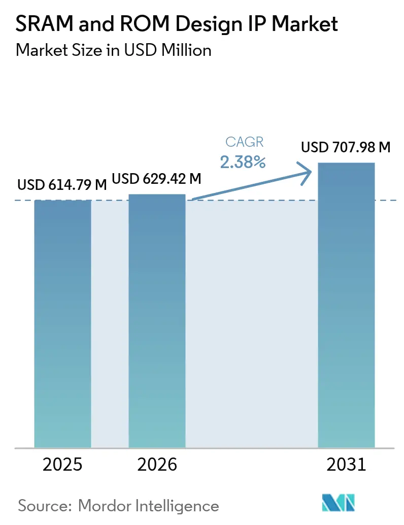
| Market Size (2026) | USD 629.42 Million |
| Market Size (2031) | USD 707.98 Million |
| Growth Rate (2026 - 2031) | 2.38 % |
| Fastest Growing Market | Asia Pacific |
| Largest Market | Asia Pacific |
| Market Concentration | Medium |
Major Players
*Disclaimer: Major Players sorted in no particular order Image © Mordor Intelligence. Reuse requires attribution under CC BY 4.0. |
|
SRAM And ROM Design IP Market Analysis by Mordor Intelligence
The SRAM and ROM Design IP market size was valued at USD 614.79 million in 2025 and estimated to grow from USD 629.42 million in 2026 to reach USD 707.98 million by 2031, at a CAGR of 2.38% during the forecast period (2026-2031). Continued demand for cache-dense AI accelerators, 5G edge nodes, and automotive functional-safety platforms underpins this measured expansion. Sub-14 nm processes capture disproportionate licensing fees as design houses seek bit-cell architectures that tame variability, leakage, and soft-error rates. Hard IP remains the preferred delivery format because it minimizes qualification risk and accelerates tape-out schedules, yet chiplet-ready memory tiles are now gaining momentum as heterogeneous packaging moves into volume production. Competitive intensity is rising as open-source compilers compress average selling prices, prompting established vendors to intensify their focus on verification suites and foundry partnerships. Regionally, the Asia Pacific dominates shipments due to its foundry scale and government subsidies, while North America sustains its innovation leadership through its fabless design ecosystem.
Key Report Takeaways
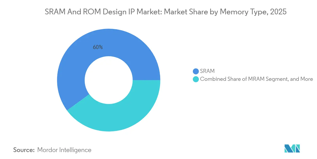
- By memory type, SRAM led with 60.05% of the SRAM and ROM Design IP market share in 2025, while embedded flash and other non-volatile options are projected to expand at a 3.72% CAGR through 2031.
- By application, consumer electronics accounted for 36.10% of the SRAM and ROM Design IP market size in 2025, whereas automotive and transportation are forecast to grow at a 4.9% CAGR during 2026-2031.
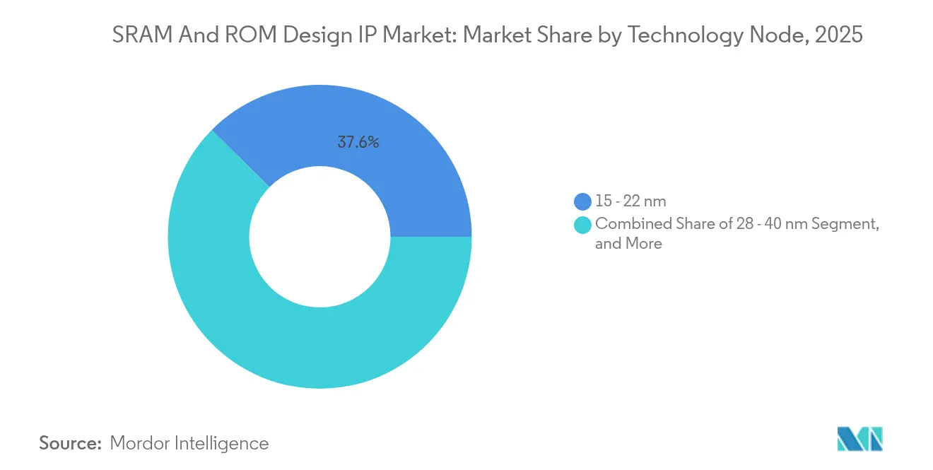
- By technology node, the 15–22 nm class held a 37.60% share of the SRAM and ROM Design IP market size in 2025, while sub-14 nm nodes are expected to advance at a 3.92% CAGR through 2031.
- By IP delivery type, hard IP captured a 47.35% share of the SRAM and ROM Design IP market in 2025; chiplet and 3D die-level IP is the fastest-rising format at a 4.22% CAGR through 2031.
- By geography, the Asia Pacific region dominated the SRAM and ROM Design IP market with 46.85% of the market revenue in 2025 and is projected to grow at a 3.82% CAGR through 2031.
Note: Market size and forecast figures in this report are generated using Mordor Intelligence’s proprietary estimation framework, updated with the latest available data and insights as of 2026.
Market Trends and Insights
Drivers Impact Analysis of SRAM And ROM Design IP Market*
| Driver | (~) % Impact on CAGR Forecast | Geographic Relevance | Impact Timeline |
|---|---|---|---|
| AI-centric SoCs pushing large on-chip cache | +0.8% | North America; Asia Pacific | Medium term (2-4 years) |
| 5G and edge-computing rollout | +0.6% | Asia Pacific; North America | Short term (≤2 years) |
| Shift from eFlash to MRAM <28 nm | +0.4% | Advanced foundry regions | Long term (≥4 years) |
| Automotive Grade-1 functional-safety rules | +0.3% | Europe; North America | Medium term (2-4 years) |
| Chiplet architectures standardizing die I/O | +0.2% | North America; Asia Pacific | Long term (≥4 years) |
| Foundry turnkey memory compilers | +0.2% | Asia Pacific | Short term (≤2 years) |
| Source: Mordor Intelligence | |||
Proliferation of AI-centric SoCs demanding large on-chip cache
Inference accelerators now integrate as much as 40 MB of SRAM to store weights and feature maps, far eclipsing the 8-16 MB found in general-purpose processors.[1]Simon Segars, “Arm Announces New CPU and GPU Designs for AI Workloads,” arm.com Compute-in-memory variants place arithmetic operations directly inside the bit cell to reduce data movement energy, creating new compiler requirements. Sovereign-AI initiatives in multiple regions add volume by funding domestic chip programs that insist on locally verified memory IP. Three-dimensional stacking through-silicon vias further raises cache ceilings while preserving the footprint. Vendors capable of shipping multi-gigahertz, low-leakage SRAM macros with exhaustive timing corners are best positioned to capitalize on this upswing.
5G and edge-computing roll-outs accelerating low-power embedded SRAM adoption
Edge servers and IoT nodes require sub-1V memory blocks that retain data across a temperature range of –40 °C to 125 °C. Next-generation IP now posts leakage below one nanoampere per megabit by combining multi-threshold transistors with power-gating cells.[2]Samsung Foundry Team, “Samsung Foundry Announces 4 nm Process Technology for 5G Applications,” samsungsemiconductor.com Dynamic body-biasing allows designers to trade standby power for access speed on a minute-to-minute basis. In parallel, 5G baseband ASICs rely on dual-port SRAM that is finely tuned for burst packet buffering. These stringent power profiles raise the bar for characterization depth and corner validation, favoring suppliers with silicon-proven data across multiple foundries.
Transition from eFlash to MRAM below 28 nm unlocking new licensing revenue streams
Embedded flash struggles with high thermal budgets and gate-oxide scaling, making it uneconomical beyond 28 nm. Foundries have therefore integrated magnetic tunnel junction stacks that permit back-end-of-line insertion with minimal impact on logic. Spin-transfer torque MRAM endures >10¹⁵ writes, eliminating flash wear-leveling overhead in automotive elements. The lengthy 18-24 month qualification cycles erect barriers that smaller houses find hard to clear. IP vendors able to supply compiler flows, macro hardening, and in-system bias drivers gain an annuity-like revenue stream as each new node migrates to MRAM.
Automotive Grade-1 functional-safety rules boosting qualified memory IP demand
ISO 26262 ASIL-D flows require dual-redundant arrays, ECC, background self-tests, and single-event upset mitigation. Radiation-tolerant bit-cells and error-detection scrubbing raise area by 10-15%, yet OEMs accept the cost to meet over-the-air update and fail-operational mandates. Qualification spans 3-5 years and involves thousands of fault-injection scenarios. Once secured, sockets typically persist for a decade of vehicle production, giving incumbents a durable share.
Restraints Impact Analysis of SRAM And ROM Design IP Market*
| Restraint | (~) % Impact on CAGR Forecast | Geographic Relevance | Impact Timeline |
|---|---|---|---|
| Open-source compilers eroding ASPs | –0.5% | Global | Short term (≤2 years) |
| ReRAM/FeRAM cannibalizing small ROM sockets | –0.3% | Consumer electronics | Medium term (2-4 years) |
| Export-control compliance hurdles for China tape-outs | –0.4% | China; global spillover | Short term (≤2 years) |
| Reliability headwinds for ≤7 nm SRAM bit-cells | –0.2% | Asia Pacific; North America | Long term (≥4 years) |
| Source: Mordor Intelligence | |||
Pricing pressure from open-source memory compilers eroding ASPs
Community projects tied to the RISC-V ecosystem now deliver free SRAM generators for mature nodes, undercutting commercial offerings in cost-sensitive wearables and toys.[3]RISC-V International, “RISC-V Memory Compiler Initiative Launches,” riscv.org Universities further seed libraries, giving fabless teams a quick path to first silicon. Vendors defend their margins by emphasizing the reduction of leakage, coverage of corners, and safety packages that open-source flows often lack. Nonetheless, entry-level revenue streams continue to compress.
Export-control compliance hurdles for Chinese tape-outs
In October 2022, U.S. rules mandated export licenses for advanced memory IP, enabling AI functions.[4]U.S. Department of Commerce, “Advanced Computing and Semiconductor Manufacturing Controls,” bis.doc.gov Approval cycles stretch deal timelines and impose documentation overhead. Some Western licensors have paused deliveries below 14 nm, prompting Chinese fabs to accelerate their in-house compiler efforts. Fragmentation reduces total addressable volume for international suppliers while raising compliance costs across the value chain.
*Our forecasts treat driver/restraint impacts as directional, not additive. The impact forecasts reflect baseline growth, mix effects, and variable interactions.
SRAM And ROM Design IP Market Segment Analysis
By Memory Type:
SRAM dominance persists as emerging NVM gains momentumSRAM retained 60.05% share of the SRAM and ROM Design IP market in 2025, a testament to its unmatched speed in cache and buffer roles. The segment climbs modestly in absolute dollars as AI accelerators and 5G switches request fatter on-die slices. In parallel, ROM families, including PROM, EPROM, and EEPROM, serve as boot code and calibration tables, but gradually shrink as system-on-chip consolidation removes discrete blocks. The SRAM and ROM Design IP market size associated with MRAM and other non-volatile newcomers remains modest, yet their position strengthens once eFlash reaches a capacity limit below 28 nm.
Licensing tied to embedded flash and alternative NVM grows at the fastest rate, with a 3.72% CAGR, because IoT microcontrollers and automotive ECUs require durable code storage. Multi-technology compilers that couple SRAM’s speed with MRAM’s persistence underpin hybrid arrays entering pilot production. Vendors versed in both volatility domains command a pricing premium, especially when they can map identical logical interfaces across processes, trimming firmware porting risk.


By Application:
Consumer electronics leadership yields to automotive growthConsumer devices held 36.10% of the SRAM and ROM Design IP market share in 2025, driven by smartphones, tablets, and consoles that demand ever-richer graphics and local AI capabilities. Design cycles remain brisk, but capacity gains plateau as vendors recycle board real estate for cameras and antennas. Telecommunications ASICs rely on dual-port SRAM tuned for <1 ns latency to maintain line-rate packet forwarding, a niche that rewards compiler flexibility.
Automotive and transportation IP bookings are projected to rise at a 4.9% CAGR to 2031, driven by the demand for advanced driver-assistance systems that require multi-gigabyte on-chip arrays paired with ASIL-D diagnostics. The SRAM and ROM Design IP market size exposed to Grade-1 functional safety, therefore, increases faster than any other vertical. Aerospace and defense requests remain small in volume, yet they yield high average selling prices because radiation-hardened libraries undergo rigorous qualification.
By Technology Node:
Mature geometries dominate volume while advanced nodes set the paceThe 15–22 nm class accounted for 37.60% of revenue in 2025, as it combines performance with established yield learning. Low-risk consumer and automotive controllers sit comfortably here, and compiler IP amortizes across several foundry variants. Above 45 nm, trailing-edge libraries persist in long-tail industrial and military programs whose redesign costs outweigh power-area savings.
Sub-14 nm macros advance at 3.92% CAGR because data-center AI accelerators, flagship smartphones, and high-performance computing chips cannot meet density or power targets on larger nodes. Each geometry shrink multiplies bit-cell variation vectors, accentuating the value of vendors that supply exhaustive PVT models and reliability monitors. The SRAM and ROM Design IP market size for these bleeding-edge nodes commands premium royalties that more than offset narrower unit volumes.
By IP Delivery Type:
Hard IP prevails while chiplet forms accelerateHard IP delivered 47.35% of the total 2025 billings. Customers appreciate its silicon-proven layouts, which shave weeks from sign-off and minimize die area. Compiler IP bridges flexibility and turnaround time yet concedes floor-plan efficiency, limiting uptake in cost-sensitive gadgets. Soft IP remains essential for users chasing exotic architectures or proprietary transistor options.
Chiplet and 3D die-level memory tiles present the liveliest sub-segment with a projected 4.22% CAGR. They let designers mix mature memory wafers with cutting-edge logic while meeting bandwidth goals through ultra-short interposer runs. Early adopters in data-center accelerators validate economic returns, encouraging wider field adoption.
Geography Analysis
APAC SRAM and ROM Design IP Market
The Asia Pacific held 46.85% of the SRAM and ROM Design IP market revenue in 2025 and is projected to grow at a 3.82% CAGR through 2031. Foundry clusters in Taiwan, South Korea, and mainland China lower tape-out costs, while national subsidy schemes bankroll indigenous compiler projects. Japan contributes safety-focused macros tailored for Tier-1 automotive suppliers and industrial robotics, reinforcing regional breadth.
North America SRAM and ROM Design IP Market
North America commands the lion’s share of bleeding-edge design starts as Silicon Valley startups and hyperscale cloud vendors race to release proprietary AI silicon. The CHIPS Act funnels fresh capital into domestic fabs, catalyzing on-shore IP verification labs and opening grant channels for smaller houses. Automotive Tier-1s in Detroit partner with aerospace primes to request radiation-hard, ASIL-D compliant macros, tapping into high-margin niches.
Europe SRAM and ROM Design IP Market
Europe focuses on automotive and industrial automation, leveraging Germany’s OEM ecosystem and stringent enforcement of ISO 26262. Nordic countries supply ultra-low-power memories for harsh environments, while France and Italy explore sovereign computing initiatives that favor local IP. Overall, continental demand tilts toward reliability and functional safety credentials over raw density.


Regulatory Landscape
Export controls and national-security measures influence how advanced SRAM/ROM IP is licensed, transferred, and supported across borders. The United States Bureau of Industry and Security (BIS) refined Export Administration Regulations controls for advanced computing integrated circuits effective January 16, 2025, adding diligence and compliance expectations that affect sub-14 nm memory IP engagements and documentation practices. BIS also clarified in guidance issued May 31, 2026 that certain license requirements can depend on an entity's headquarters (including Country Group D:5 and Macau) rather than only physical location, which increases the importance of screening, end-use checks, and contract clauses across global tape-out and support workflows.
Standards work also shapes integration and verification requirements for design IP users. IEC published IEC 62014-4:2025 (IP-XACT) in June 2025, providing a recognized framework for describing and integrating IP, while JEDEC updates such as JESD209-6 (LPDDR6, July 2025) and JESD239E (GDDR7 SGRAM, May 2026) point to evolving memory interface ecosystems that can tighten compatibility expectations across adjacent controller, PHY, and verification collateral. In parallel, U.S. policy actions addressing semiconductor import risks, including a January 2026 proclamation outlining a two-phase plan and referencing a 25% ad valorem tariff on specific semiconductor categories, add another layer of cost and classification attention for globally distributed design and manufacturing programs.
Value Chain Analysis
The SRAM/ROM design IP value chain begins with architecture, bit-cell design, characterization, and verification, then moves into SoC/ASIC integration using EDA platforms, and finally to foundry enablement and silicon validation on target process nodes. Core participants include IP suppliers (SRAM macros, ROM/OTP, and memory compilers), EDA vendors such as Synopsys and Cadence for implementation and sign-off flows, and foundries such as TSMC and Samsung Foundry, which co-develop PDK-qualified memory generators and reference flows. Advanced-node delivery typically emphasizes silicon-proven hard IP and foundry-certified collateral to reduce qualification risk, while mature-node programs rely more on compiler-based parameterization and face increasing pressure from open-source generators.
Commercialization is usually structured around an upfront technology license fee plus royalties or per-unit fees, and buyers increasingly qualify second-source compilers and libraries to reduce dependency risk, particularly for complex nodes below 7 nm. The chain also reflects upstream manufacturing chokepoints, including advanced equipment such as EUV tools, which constrain leading-edge wafer output and can influence which nodes see the most near-term tape-outs and which memory IP portfolios monetize first. As packaging and multi-die design become more common, handoffs broaden to include chiplet/3D integration requirements, tighter interface compliance, and expanded verification workloads across vendors and foundry partners.
Competitive Landscape
The field shows moderate consolidation. A handful of suppliers cover every mainstream node from 180 nm down to 3 nm and offer bundled verification IP, scripting flows, and silicon statistics. These leaders exploit scale to pre-tape‐out macros on new processes in partnership with foundries, enabling “Day-1” availability that emerging rivals struggle to match. Pricing disciplines erode as open-source projects commoditize mature nodes, so incumbents lean into automotive and AI verticals where safety and power budgets amplify differentiation.
Strategic moves underscore this path. Arm acquired Intrinsix for USD 85 million in September 2024 to deepen its AI-tuned SRAM expertise. Synopsys added Verific Design Automation for USD 120 million the previous month, knitting formal verification engines into its compiler chain. Foundries, meanwhile, roll out in-house macro generators that pull IP vendors closer via joint PDK enablement.
White-space opportunities emerge in compute-in-memory SRAM for edge inference, UCIe-compliant chiplets for data center accelerators, and MRAM arrays for over-the-air automotive updates. Suppliers able to certify both ASIL-D flows and export-control coverage lock in long-cycle demand. Market share, nevertheless, remains fluid as new memory physics, such as ReRAM, threaten to displace entrenched bit cells.
SRAM And ROM Design IP Industry Leaders
-
Arm Ltd.
-
Synopsys Inc.
-
Cadence Design Systems Inc.
-
Siemens EDA (Mentor Graphics Corporation)
-
eMemory Technology Inc.
- *Disclaimer: Major Players sorted in no particular order

SRAM And ROM Design IP Market Companies Covered in this Report
- Arm Ltd.
- Synopsys Inc.
- Cadence Design Systems Inc.
- Siemens EDA (Mentor Graphics Corporation)
- eMemory Technology Inc.
- Silvaco Inc.
- Dolphin Design SAS
- VeriSilicon Holdings Co. Ltd.
- SureCore Ltd.
- Xilinx Inc.
- Renesas Electronics Corporation
- Everspin Technologies Inc.
- Avalanche Technology Inc.
- TDK Corporation
- Kilopass Technology Inc.
- Silicon Storage Technology Inc.
- GSI Technology Inc.
- Dolphin Technology Inc.
- TekStart LLC
- Flex Logix Technologies Inc.
- Rambus Inc.

Market Opportunities and Future Outlook
Whitespace is developing around tightly integrated security and non-volatile boot or storage functions that sit next to SRAM/ROM usage in modern SoCs, particularly where secure provisioning and patch mechanisms are required. Memory IP providers that can bundle ROM, OTP, and hardware-root-of-trust capabilities with integration collateral benefit from pull across secure key storage and secure update flows in AI accelerators, automotive platforms, and IoT designs, where SRAM caches and ROM/OTP blocks are designed alongside verification and compliance requirements.
Opportunity also concentrates at the ends of the node mix: leading-edge programs that require validated, multi-die ready collateral, and differentiated mature-node platforms tuned for power management and long lifecycle products. Demand for fresh memory architectures and characterized compilers shows up in alternative SRAM-like approaches and advanced-node qualification activities for 2 nm-class processes, including RAAAM Memory Technologies taping out a customer test chip on a 2 nm node (March 2026) and partnering with Avnet ASIC to develop and qualify GCRAM on TSMC 2 nm (June 2026). On established nodes, platform-oriented enablement continues to create sockets for SRAM and ROM IP tied to specific use cases, such as M31 Technology cooperating with Tower Semiconductor to develop SRAM and ROM solutions for a 65 nm power management platform (August 2024), supporting long-run industrial and mixed-signal design programs that prioritize reliability and integration speed.
Recent Industry Developments in SRAM And ROM Design IP Market
- May 2026: Siemens reported use of its Veloce Strato CS hardware-assisted verification platform to validate the Arm AGI CPU built on the Arm Neoverse CSS V3 platform. This puts added emphasis on pre-silicon validation capacity for complex AI-class designs, where embedded SRAM/ROM subsystems and their verification collateral must meet timing, power, and functional targets across multi-die and advanced-node contexts.
- May 2025: JEDEC published JESD209-6 (LPDDR6), extending the roadmap for low-power DRAM signaling and platform requirements. While LPDDR6 is not SRAM/ROM IP, the standard update increases integration and verification complexity for SoCs that combine on-chip SRAM with external memory subsystems, pushing IP teams to deliver cleaner interoperability collateral and compliance-ready deliverables.
- June 2024: Samsung Foundry partnered with Cadence on ISO 26262 ASIL-D qualified memory IP for advanced driver-assistance systems. The partnership reinforces the premium placed on safety-ready embedded memory macros and validation flows, strengthening demand for qualified SRAM/ROM IP packages aligned to automotive functional-safety requirements.


SRAM And ROM Design IP Market Report Scope and Research Methodology
Market Definition and Coverage
This market measures revenues earned from licensing and delivering SRAM and ROM memory design IP used inside semiconductor chips, including embedded memory IP delivered as hard, soft, or compiler-based blocks across major end-use chip programs worldwide.
Scope exclusions: We exclude revenue from physical wafer fabrication, standalone memory chip sales, EDA tool subscriptions, and general design services that are not tied to memory IP licensing or royalties.
Segments Covered in This Report
-
By Memory Type
- SRAM
- ROM (PROM / EPROM / EEPROM)
- MRAM
- Embedded Flash / Other NVM
-
By Application
- Consumer Electronics
- Telecommunications and Networking
- Automotive and Transportation
- Industrial and IoT
- Aerospace and Defense
- Other Applications
-
By Technology Node
- ≤14 nm
- 15 – 22 nm
- 28 – 40 nm
- ≥45 nm
-
By IP Delivery Type
- Hard IP
- Soft IP
- Parameterised Compiler IP
- Chiplet / 3D Die-level IP
-
By Geography
-
North America
- United States
- Canada
- Mexico
-
South America
- Brazil
- Argentina
- Rest of South America
-
Europe
- Germany
- United Kingdom
- France
- Italy
- Spain
- Rest of Europe
-
Asia Pacific
- China
- Japan
- India
- South Korea
- South-East Asia
- Rest of Asia Pacific
-
Middle East
- Saudi Arabia
- United Arab Emirates
- Turkey
- Rest of Middle East
-
Africa
- South Africa
- Nigeria
- Rest of Africa
-
North America
Data Sources, Market Sizing, and Validation
Desk Research
Desk work starts by mapping what drives demand for embedded SRAM and ROM blocks across logic chips, then linking those drivers to value capture through licensing and royalty models. We use public indicators such as semiconductor industry shipments and revenue splits, pulled from sources like World Semiconductor Trade Statistics, USITC trade statistics, OECD indicators, and IMF macro series, to keep the demand backdrop consistent with the broader cycle.
To anchor technology movement, we also review open sources such as IEEE and ACM publications, patent databases, and standards or guidance materials connected to automotive safety and security requirements that influence memory usage in SoCs. Company filings, earnings call transcripts, investor decks, and reputable press are used to understand mix shifts between hard IP and soft IP, and how leading-edge nodes can change typical pricing. Where needed, a paid subscription focused on company financials and a patent database subscription are used to keep revenue splits and innovation signals consistent across years. The sources listed above are illustrative, and additional public documents and data series were reviewed to clarify assumptions and run cross-checks.
Primary Interviews and Surveys
Primary work was used to pressure-test how memory IP is priced and delivered across technology nodes, and to confirm how SRAM and ROM blocks are typically used across major chip programs. We spoke with a mix of IP suppliers, semiconductor design teams, and ecosystem participants across APAC, EMEA, and the Americas, so regional tape-out intensity and global licensing patterns were reflected in the final model.
Distribution of primary research fieldwork respondents
| Company type | Respondent position | Region |
|---|---|---|
| Top tier: 35% | CXOs: 12% | APAC: 41% |
| Mid tier: 48% | Functional/Unit leaders: 32% | EMEA: 37% |
| Smaller Players: 17% | Managers: 56% | Americas: 22% |
Market-Sizing & Forecasting
The core build uses top-down and bottom-up logic, where semiconductor design activity is reconstructed by region and end-use, and then filtered into the addressable pool for embedded SRAM and ROM design IP based on typical SoC content. Once the demand pool is formed, pricing is applied using licensing fees, royalties, and one-time delivery charges, which tend to vary by technology node and IP delivery type.
Key inputs in this market include the mix shift toward advanced nodes (such as 14 nm and below), the share of hard IP versus soft or compiler IP, the pace of SoC shipments in high-memory applications (AI accelerators, networking equipment, and automotive compute), and the cadence of new design starts tied to tape-outs. To keep totals grounded, results are cross-checked with selective bottom-up approximations, such as sampled ASP by node multiplied by estimated design program counts, followed by channel checks on typical royalty ranges. When visibility is weaker for smaller design houses, gaps are handled using conservative attachment-rate bands validated in interviews, and those bands are only widened when multiple respondents align.
For forecasting, scenario analysis is used so node migration speed, design-start momentum, and price progression for embedded SRAM macros can be flexed without breaking the model. The forward view is then aligned to what interviewees expect for end-market demand and near-term design activity by region.
Data Validation & Update Cycle
Outputs are checked against independent signals, such as broad semiconductor revenue growth, regional design activity cues, and visible shifts in technology-node adoption, and unusual jumps are reviewed line by line. We also run variance checks across regions and IP delivery types so one assumption does not quietly drive the total market in an unrealistic way.
Before sign-off, the model and assumptions go through multiple analyst reviews, and respondents are re-contacted when pricing ranges, node mix, or end-market demand signals move outside expected bounds. Reports are refreshed annually, with interim updates when material events can change near-term demand, and a final pre-delivery pass is completed so clients receive the latest updated view.
Mordor Intelligence's Global Sram and Rom Design Ip Market Size Compared Against Other Published Estimates
Published market sizes for SRAM and ROM design IP can vary even when the topic name looks similar, because firms draw scope lines differently around licensing revenues and they also use different timing for currency conversion and year labeling. The same demand backdrop can therefore translate into a different value, depending on what is counted and how pricing is projected.
By tracking delivery-type mix (hard IP versus soft and compiler IP), node-based pricing bands, and annual refresh triggers, Mordor Intelligence keeps the total aligned to SRAM and ROM design IP licensing and royalties, instead of blending in EDA subscriptions or unrelated design service revenue. The biggest gaps usually come from whether adjacent embedded non-volatile memory IP categories are included, how aggressively next-node adoption is assumed, and whether royalty-bearing deployments are estimated using a single proxy rather than several end-market checks.
Benchmark comparison
| Source | Market Size | Gaps in Research Methodology |
|---|---|---|
| Mordor Intelligence | USD 629.42 M (2026) | |
| Global Consultancy A | USD 0.88 B (2026) | This estimate appears to widen scope by rolling multiple semiconductor IP categories together, which can pull in revenue that is not specific to SRAM and ROM memory IP licensing or royalties. |
| Trade Journal B | USD 0.49 B (2026) | This estimate seems to apply conservative node-mix and pricing assumptions and may restrict royalty-bearing deployments, which can undercount high-volume SoC programs that embed multiple SRAM macros. |
The spread in values is mainly explained by what is treated as in-scope revenue and how node mix and pricing are carried into the stated year. A model that ties demand to design activity, applies transparent licensing and royalty logic, and cross-checks totals with interview-backed ranges tends to land closer to the practical spend created by chip programs.


Key Questions Answered in the Report
How big is the SRAM and ROM Design IP market today?
The SRAM and ROM Design IP market size stands at USD 629.42 million in 2026 and is on track to reach USD 707.98 million by 2031.
Which segment is expanding the fastest?
Embedded flash and other non-volatile memory IP post the highest growth at a 3.72% CAGR through 2031 thanks to IoT and automotive demand.
Why is Asia Pacific so dominant?
Foundry scale, government subsidies, and a concentration of design houses give Asia Pacific 46.85% share and sustained 3.82% CAGR growth.
How are chiplet trends reshaping memory IP?
Chiplet-ready memory tiles paired with UCIe links are growing at a 4.22% CAGR because they let designers mix node choices while boosting bandwidth.
What keeps pricing under pressure?
Open-source SRAM compilers and university-backed libraries are eroding entry-level ASPs, forcing commercial vendors to emphasize power, safety, and verification depth.
Which regulatory issue impacts China-based designs?
U.S. export-control rules imposed in 2022 require licenses for advanced SRAM and emerging memory IP, lengthening deal cycles and motivating domestic alternatives.
Page last updated on:


 Your data is secure and never sold or shared.


