| Study Period | 2019 - 2030 |
| Market Size (2025) | USD 11.47 Billion |
| Market Size (2030) | USD 25.37 Billion |
| CAGR (2025 - 2030) | 17.20 % |
| Fastest Growing Market | Asia Pacific |
| Largest Market | Asia Pacific |
| Market Concentration | Medium |
Major Players*Disclaimer: Major Players sorted in no particular order |


2.5D and 3D Semiconductor Packaging Market Analysis
The 2.5D & 3D Semiconductor Packaging Market size is estimated at USD 11.47 billion in 2025, and is expected to reach USD 25.37 billion by 2030, at a CAGR of 17.2% during the forecast period (2025-2030).
The semiconductor packaging industry is witnessing a fundamental shift as traditional scaling limitations and increasing fabrication costs of advanced nodes drive the adoption of modular design approaches. This transformation is particularly evident in the defense sector, where semiconductor applications are expanding rapidly due to increasing military modernization efforts. According to the US Congressional Budget Office, defense spending in the United States amounted to USD 746 billion in 2023 and is forecast to reach USD 1.1 trillion by 2033. The integration of advanced semiconductor packaging in military applications spans various domains, including radar systems, electronic warfare equipment, and advanced communication systems, driving the need for more sophisticated packaging solutions.
The industry is experiencing a significant transformation through heterogeneous integration packaging technologies, enabling the combination of different chips into unified systems. This trend is particularly evident in the data center and high-performance computing sectors, where the demand for increased processing power and reduced latency is paramount. The semiconductor industry demonstrated its robust growth trajectory with global sales reaching USD 137.7 billion during the first quarter of 2024, reflecting a 15.2% increase compared to the first quarter of 2023. This growth is largely attributed to the increasing adoption of advanced semiconductor packaging solutions that enable higher performance and improved power efficiency.
The proliferation of connected devices and the Internet of Things (IoT) is reshaping the semiconductor packaging landscape. According to Cisco's analysis, IoT devices constituted 50% (14.7 billion) of all networked devices in 2023, marking a significant increase from previous years. This surge in connected devices has led to increased demand for advanced IC packaging solutions that can accommodate multiple functionalities while maintaining smaller form factors. The industry is responding with innovations in packaging technologies that enable the integration of various components, including sensors, processors, and memory, in increasingly compact designs.
Major industry players are making substantial investments in advanced packaging capabilities to meet evolving market demands. In November 2023, Samsung Electronics announced the development of SAINT (Samsung Advanced Interconnection Technology), a new advanced 3D chip packaging technology comprising three variants - SAINT D, SAINT L, and SAINT S. Similarly, TSMC has expanded its advanced packaging portfolio with innovations like CoWoS-R and SoIC technology. These developments are particularly significant for applications in artificial intelligence, where high-performance computing capabilities are crucial. According to Ericsson's projections, the increasing digitalization trend is expected to drive smartphone subscriptions to reach 7.7 billion by 2028, further emphasizing the need for system-in-package solutions in consumer electronics.
2.5D and 3D Semiconductor Packaging Market Trends
Growing Consumption of Semiconductor Devices Across Industries
The semiconductor industry is experiencing unprecedented demand across multiple sectors, driven by the rapid digitization of industries and increasing adoption of advanced technologies. According to the Semiconductor Industry Association, worldwide semiconductor sales showed strong momentum, reaching USD 47.63 billion in January 2024, with consistent growth through late 2023 and early 2024. This surge in demand is particularly evident in the automotive sector, where the transition to electric vehicles has significantly increased semiconductor content per vehicle. For instance, according to Kelley Blue Book, over 1.18 million new electric vehicles entered the U.S. market in 2023, highlighting the expanding semiconductor requirements in modern vehicles.
The proliferation of Internet of Things (IoT) devices has become a major driver for semiconductor consumption across industries. According to Ericsson's projections, the number of short-range IoT devices is expected to reach 25 billion by 2027, while wide-area IoT devices are predicted to grow to 5.4 billion in the same period. This explosive growth in connected devices is complemented by the rapid expansion of 5G infrastructure, with GSMA reporting that 5G networks are expected to cover one-third of the world's population by 2025. The advancement in data centers and cloud computing facilities has also intensified semiconductor demand, with major economies like China hosting 448 data centers as of 2023, followed by Australia with 306 and Japan with 218 facilities, demonstrating the robust infrastructure development supporting digital transformation.
Understand The Key Trends Shaping This Market
Download PDF
Increasing Demand for Compact, High Functionality Electronic Devices
The consumer technology landscape is witnessing a significant shift toward more compact and multifunctional electronic devices, driving innovation in advanced semiconductor packaging technologies. According to the Consumer Technology Association (CTA), retail revenue from consumer technology is projected to grow 2.8% to USD 512 billion in 2024, indicating strong market demand for advanced electronic devices. This trend is particularly evident in the proliferation of smart wearables, mobile devices, and IoT-enabled products that require increasingly sophisticated semiconductor solutions to deliver enhanced functionality while maintaining compact form factors.
The integration of artificial intelligence and advanced computing capabilities in everyday devices has further accelerated the need for compact, high-performance semiconductor packaging solutions. This is exemplified by the growing adoption of high-bandwidth memory (HBM) and advanced processing units in modern devices. Major industry players are responding to these demands with innovative solutions. For instance, in November 2023, Samsung Electronics unveiled an advanced three-dimensional chip packaging technology called SAINT (Samsung Advanced Interconnection Technology) to integrate memory and processors required for high-performance chips, including AI chips, in much smaller sizes. Similarly, TSMC's introduction of the 3Dblox 2.0 open standard in September 2023 demonstrates the industry's commitment to advancing 3D IC design capabilities, specifically targeting the growing demand for compact, high-performance electronic devices. The use of high-density packaging and through-silicon via packaging is becoming increasingly prevalent to meet these demands, ensuring that devices are both powerful and efficient. Furthermore, the adoption of system-in-package and advanced IC packaging technologies is crucial in supporting the miniaturization and integration trends observed in the industry.
Segment Analysis: By Packaging Technology
3D Segment in 2.5D & 3D Semiconductor Packaging Market
The 3D segment dominates the 2.5D & 3D semiconductor packaging market, commanding approximately 63% market share in 2024 while also being the fastest-growing segment with a projected growth rate of around 18% during 2024-2029. This segment's leadership position is driven by its ability to achieve higher-density integration by stacking multiple layers of silicon dies, which is crucial for applications like smartphones, wearables, and Internet of Things (IoT) devices. The technology enables a reduced data transmission time between chips compared to existing wire bonding technology, resulting in significantly lower power consumption and faster speed. The small size of the through-silicon via packaging addresses the miniaturization requirements in wearable products, while also providing enhanced functionality through the tight integration of multiple dies on a die-to-die substrate. Major industry players like Samsung Electronics, TSMC, and Intel Corporation have made significant investments in advancing 3D packaging capabilities, particularly for high-performance computing and AI applications.
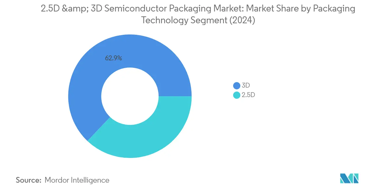
2.5D Segment in 2.5D & 3D Semiconductor Packaging Market
The 2.5D packaging technology represents a significant portion of the market, offering a versatile and high-performance solution for integrating multiple dies within a single package. This technology combines multiple integrated circuits onto a single substrate, known as an interposer, to enhance performance, integration, and efficiency. The interposer, typically made of silicon, glass, or organic material, serves as a platform onto which multiple dies are placed, featuring fine wiring to connect various dies together. The technology has gained particular traction in high-performance computing applications, especially in data centers and AI implementations, where it provides the performance and efficiency required for these demanding use cases. The growing adoption of high-performance computing in various sectors, including data centers, AI, and machine learning, continues to drive the demand for 2.5D packaging solutions, including silicon interposer technology.
Segment Analysis: By End-User Industry
Consumer Electronics Segment in 2.5D & 3D Semiconductor Packaging Market
The consumer electronics segment dominates the 2.5D & 3D semiconductor packaging market, commanding approximately 65% of the market share in 2024. This significant market position is driven by the increasing adoption of advanced electronic devices, particularly smartphones, gaming consoles, and wearable technology. The segment's growth is further supported by the rising penetration of 5G technology, with GSMA projecting 5G networks to cover one-third of the world's population by 2025. The demand for miniaturization and enhanced performance in consumer devices continues to fuel the need for advanced packaging solutions, such as 3D IC packaging. The integration of artificial intelligence features in various consumer electronics devices, including PCs and smartphones, has created additional opportunities for market expansion. Furthermore, the trend towards smart homes and IoT devices has significantly contributed to the segment's dominance, with Cisco reporting that IoT devices constituted approximately 50% of all networked devices in 2023.
Communications and Telecom Segment in 2.5D & 3D Semiconductor Packaging Market
The communications and telecom segment is emerging as the fastest-growing sector in the 2.5D & 3D semiconductor packaging market, with a projected CAGR of approximately 24% during 2024-2029. This remarkable growth is primarily driven by the explosive increase in data generation worldwide and the rapid deployment of 5G infrastructure. The segment's expansion is further accelerated by the growing adoption of high-performance computing (HPC) solutions, which require enhanced semiconductor packaging for improved performance and power efficiency. The increasing demand for network switches, routers, and data center equipment has created a substantial market for advanced packaging solutions, particularly in integrating High-Bandwidth Memory (HBM) components. The deployment of 5G technology has intensified the need for sophisticated packaging solutions that can manage higher frequencies and data rates while maintaining optimal power consumption and thermal management. Additionally, the segment's growth is supported by the ongoing digital transformation across industries and the increasing requirements for advanced telecommunications infrastructure to support emerging technologies such as edge computing and artificial intelligence applications, utilizing system-in-package solutions.
Remaining Segments in End-User Industry
The automotive, medical devices, and other end-user industries segments collectively represent significant opportunities in the 2.5D & 3D semiconductor packaging market. The automotive sector is experiencing substantial growth driven by the increasing adoption of electric vehicles and advanced driver assistance systems (ADAS), requiring sophisticated semiconductor packaging solutions for power electronics and sensor integration. The medical devices segment is benefiting from the growing trend of miniaturization in medical equipment and the rising adoption of connected healthcare devices, particularly in remote patient monitoring applications. Other end-user industries, including aerospace and defense, are also contributing to market growth through their increasing demand for high-performance computing solutions and advanced electronic systems. These segments are characterized by their unique requirements for reliability, performance, and specialized packaging solutions that can withstand challenging operating environments, including FOWLP technologies.
2.5D & 3D Semiconductor Packaging Market Geography Segment Analysis
2.5D & 3D Semiconductor Packaging Market in Taiwan
Taiwan dominates the global advanced semiconductor packaging market, commanding approximately 44% of the market share in 2024. The country's prominence in this sector is largely attributed to its robust semiconductor industrial ecosystem and the presence of major industry players like TSMC. The growth of Taiwan's digital economy, particularly in meeting customer demands for high-performance computing (HPC), artificial intelligence (AI), and mobile applications, has created significant opportunities for the 2.5D and 3D semiconductor packaging market. The country's manufacturers have demonstrated remarkable capabilities in producing and exporting advanced semiconductor packaging solutions through contract manufacturing for multinational companies. Taiwan's strategic position is further strengthened by continuous investments in research and development, particularly in advanced semiconductor packaging technologies. The country's semiconductor packaging industry benefits from a well-established supply chain, skilled workforce, and supportive government policies that promote technological innovation and industrial growth.
2.5D & 3D Semiconductor Packaging Market in China
China's 2.5D & 3D semiconductor packaging market is poised for remarkable expansion, with a projected CAGR of approximately 18% from 2024 to 2029. The country's semiconductor packaging industry is experiencing rapid transformation, driven by substantial government investments and private sector initiatives aimed at strengthening the domestic semiconductor ecosystem. China's large manufacturing capabilities, coupled with its existing industrial infrastructure, provide a solid foundation for market growth. The country's focus on developing energy-efficient electronic devices and the increasing demand for chiplet packaging solutions in various sectors, including consumer electronics and automotive applications, continues to drive market expansion. The establishment of new state-backed semiconductor investment funds and the development of domestic chip manufacturing capabilities demonstrate China's commitment to becoming self-sufficient in semiconductor technology. The market is further bolstered by the presence of key manufacturing facilities and research centers dedicated to advancing packaging technologies.
2.5D & 3D Semiconductor Packaging Market in United States
The United States maintains a significant position in the advanced semiconductor packaging market, driven by its advanced technological infrastructure and innovative ecosystem. The country's market is characterized by substantial investments in research and development, particularly in advanced packaging technologies for high-performance computing and artificial intelligence applications. The implementation of the CHIPS Act has created a favorable environment for domestic semiconductor manufacturing and packaging capabilities, attracting significant investments from both local and international players. The growing demand for advanced packaging solutions in various sectors, including consumer electronics, automotive, and telecommunications, continues to drive market growth. The United States' strong focus on developing domestic semiconductor capabilities, coupled with strategic partnerships with global semiconductor leaders, positions it well for sustained growth in the advanced packaging segment.
2.5D & 3D Semiconductor Packaging Market in Korea
Korea's 2.5D & 3D semiconductor packaging market is characterized by its strong technological foundation and the presence of major industry players like Samsung Electronics. The country's market benefits from significant investments in research and development, particularly in advanced packaging technologies for next-generation electronic devices. Korea's semiconductor packaging industry is closely aligned with its strong position in consumer electronics and automotive sectors, driving continuous innovation in packaging solutions. The country's focus on developing advanced packaging technologies for artificial intelligence and high-performance computing applications has created new opportunities for market growth. Korea's strategic initiatives in cloud computing and digital transformation, coupled with its robust manufacturing capabilities, continue to strengthen its position in the global semiconductor packaging landscape.
2.5D & 3D Semiconductor Packaging Market in Other Countries
The 2.5D & 3D semiconductor packaging market extends beyond the major players to include several other significant regions and countries. Japan maintains a strong presence in the market with its advanced manufacturing capabilities and focus on automotive and consumer electronics applications. European countries, particularly Germany and France, are making substantial investments in semiconductor packaging technologies, driven by their automotive and industrial sectors. The market is also seeing emerging opportunities in countries like Singapore and Malaysia, which are developing their semiconductor manufacturing and packaging capabilities. These regions benefit from various factors including government support, technological expertise, and strategic partnerships with global semiconductor leaders. The diverse landscape of the global semiconductor packaging market continues to evolve, with different regions contributing unique strengths and capabilities to the industry's growth.
Get Analysis on Important Geographic Markets
Download PDF
2.5D and 3D Semiconductor Packaging Industry Overview
Top Companies in 2.5D & 3D Semiconductor Packaging Market
The market is characterized by the presence of major players, including ASE Group, Amkor Technology, Intel Corporation, Samsung Electronics, TSMC, SPIL, Powertech Technology, JCET, GlobalFoundries, and Tezzaron Semiconductor. These companies are heavily investing in research and development to advance their advanced semiconductor packaging technologies, with a particular focus on heterogeneous integration packaging and high-performance computing applications. Strategic collaborations and partnerships have become increasingly common, as evidenced by joint ventures between foundries and packaging specialists to develop innovative solutions. Companies are expanding their manufacturing footprint globally, with significant investments in new facilities across Asia, North America, and Europe to meet growing demand and ensure supply chain resilience. The industry has witnessed a strong push towards developing proprietary packaging platforms, such as Intel's EMIB, Samsung's I-Cube, and TSMC's 3DFabric, demonstrating the competitive drive to differentiate through technological advancement.
Consolidation and Integration Drive Market Evolution
The market structure exhibits a moderate level of consolidation, with established global players dominating the advanced IC packaging segment while maintaining significant barriers to entry through their technological capabilities and capital investments. The landscape is characterized by a mix of integrated device manufacturers (IDMs) who perform packaging in-house and outsourced semiconductor assembly and test (OSAT) providers who specialize in packaging services. Major foundries have increasingly moved into the advanced packaging space, creating a more competitive environment and pushing traditional OSATs to enhance their technological capabilities and service offerings. The industry has witnessed vertical integration trends, with larger players acquiring smaller specialized firms to expand their technological portfolios and geographical presence.
The market has seen significant merger and acquisition activity, driven by the need to acquire advanced technologies and expand manufacturing capabilities. Companies are pursuing strategic acquisitions to gain access to new markets, enhance their technological capabilities, and achieve economies of scale. The trend towards consolidation is particularly evident in Asia, where major players are strengthening their positions through strategic partnerships and acquisitions. This consolidation trend is expected to continue as companies seek to build comprehensive packaging solutions and maintain competitiveness in an increasingly complex technological landscape.
Innovation and Adaptability Key to Success
Success in the market increasingly depends on companies' ability to develop and commercialize advanced packaging solutions that address the growing demands of high-performance computing, artificial intelligence, and 5G applications. Incumbent players must focus on continuous innovation in their packaging technologies, invest in research and development, and maintain strong relationships with key customers in the semiconductor industry. Companies need to demonstrate operational excellence and flexibility in their manufacturing processes while maintaining cost competitiveness. The ability to offer comprehensive solutions that integrate different packaging technologies and serve various end-user applications has become crucial for maintaining market leadership.
For new entrants and smaller players, success lies in identifying and focusing on specific market niches where they can develop specialized expertise and competitive advantages. Companies must build strong partnerships with foundries and design houses while investing in emerging technologies that could disrupt traditional packaging approaches, such as chiplet packaging. The regulatory environment, particularly regarding export controls and technology transfers, continues to influence market dynamics and company strategies. Players must also consider the increasing importance of sustainability and environmental compliance in their operations and product development. The concentration of end-users in specific regions and industries requires companies to maintain strong customer relationships and adapt their offerings to meet evolving requirements while managing potential risks from economic and geopolitical factors.
2.5D and 3D Semiconductor Packaging Market Leaders
-
ASE Group
-
Amkor Technology Inc.
-
Intel Corporation
-
Samsung Electronics Co. Ltd
-
Siliconware Precision Industries Co. Ltd (SPIL)
- *Disclaimer: Major Players sorted in no particular order

Need More Details on Market Players and Competiters?
Download PDF
2.5D and 3D Semiconductor Packaging Market News
- February 2024: Ansys and Intel Foundry partnered to offer Multiphysics signoff solutions for Intel's advanced 2.5D chip assembly technology. This technology utilizes EMIB technology to connect the die flexibly without using through-silicon via (TSVs). Ansys' precise simulation engines provide improved speeds, reduced power consumption, and increased reliability in sophisticated silicon systems for artificial intelligence (AI), high-performance computing, autonomous driving, and graphic processing.
- November 2023: Samsung Electronics was preparing to launch a new advanced 3D chip packaging technology called SAINT (Samsung Advanced Interconnection Technology) to compete with Taiwan Semiconductor Manufacturing Company's (TSMC) dominance in the market. The SAINT technology consists of three variants - SAINT D, SAINT L, and SAINT S - each aimed at improving the performance and integration of memory and processors for high-performance chips, particularly those utilized in AI applications.
2.5D & 3D Semiconductor Packaging Market Report - Table of Contents
1. INTRODUCTION
- 1.1 Study Assumptions and Market Definition
- 1.2 Scope of the Study
2. RESEARCH METHODOLOGY
3. EXECUTIVE SUMMARY
4. MARKET INSIGHTS
- 4.1 Market Overview
-
4.2 Industry Attractiveness - Porter's Five Forces Analysis
- 4.2.1 Bargaining Power of Suppliers
- 4.2.2 Bargaining Power of Buyers
- 4.2.3 Threat of New Entrants
- 4.2.4 Threat of Substitutes
- 4.2.5 Intensity of Competitive Rivalry
- 4.3 Value Chain Analysis
- 4.4 Analysis of Macroeconomic Trends on the Market
5. MARKET DYNAMICS
-
5.1 Market Drivers
- 5.1.1 Growing Consumption of Semiconductor Devices Across Several Industries
- 5.1.2 Increasing Demand for Compact, High Functionality Electronic Devices
-
5.2 Market Restraints
- 5.2.1 High Initial Investment and Increasing Complexity of Semiconductor IC Designs
-
5.3 Market Opportunities
- 5.3.1 Growing Adoption of High-end Computing, Servers, and Data Centers
6. MARKET SEGMENTATION
-
6.1 By Packaging Technology
- 6.1.1 3D
- 6.1.2 2.5D
- 6.1.3 3D Wafer-level chip-scale packaging (WLCSP) - Qualitative Analysis
-
6.2 By End-user Industry
- 6.2.1 Consumer Electronics
- 6.2.2 Medical Devices
- 6.2.3 Communications and Telecom
- 6.2.4 Automotive
- 6.2.5 Other End-user Industries
-
6.3 By Geography***
- 6.3.1 United States
- 6.3.2 China
- 6.3.3 Taiwan
- 6.3.4 South Korea
- 6.3.5 Japan
- 6.3.6 Europe
- 6.3.7 Latin America
- 6.3.8 Middle East & Africa
7. COMPETITIVE LANDSCAPE
-
7.1 Company Profiles*
- 7.1.1 ASE Group
- 7.1.2 Amkor Technology Inc.
- 7.1.3 Intel Corporation
- 7.1.4 Samsung Electronics Co. Ltd
- 7.1.5 Siliconware Precision Industries Co. Ltd (SPIL)
- 7.1.6 Powertech Technology Inc.
- 7.1.7 Jiangsu Changjiang Electronics Technology Co. Ltd
- 7.1.8 TSMC Limited
- 7.1.9 GlobalFoundries Inc.
- 7.1.10 Tezzaron Semiconductor Corporation.
8. INVESTMENT ANALYSIS
9. FUTURE OUTLOOK OF THE MARKET
**Subject to Availability
***In the final report, Latin America and Middle East and Africa will be considered together as 'Rest of the World'
You Can Purchase Parts Of This Report. Check Out Prices For Specific Sections
Get Price Break-up Now
2.5D & 3D Semiconductor Packaging Industry Segmentation
2.5D/3D is a packaging methodology for having multiple ICs inside the package. In a 2.5D structure, two or more active semiconductor chips are positioned side-by-side on a silicon interposer to reach extremely high die-to-die interconnect density. In a 3D structure, active chips are combined by die stacking for the shortest interconnect and smallest package footprint. In recent years, 2.5D and 3D have gained momentum as ideal chipset integration platforms due to their merits in achieving extremely high packaging density and energy efficiency.
The 2.5D and 3D semiconductor packaging market is segmented by packaging technology (3D, 2.5D, 3D wafer-level chip-scale packaging (WLCSP) - Qualitative Analysis), end-user industry (consumer electronics, medical devices, communications and telecom, automotive, and other end-user industries), geography (United States, China, Taiwan, Korea, Japan, Europe, and the Rest of the World). The report offers the market size in value terms in USD for all the abovementioned segments.
| By Packaging Technology | 3D |
| 2.5D | |
| 3D Wafer-level chip-scale packaging (WLCSP) - Qualitative Analysis | |
| By End-user Industry | Consumer Electronics |
| Medical Devices | |
| Communications and Telecom | |
| Automotive | |
| Other End-user Industries | |
| By Geography*** | United States |
| China | |
| Taiwan | |
| South Korea | |
| Japan | |
| Europe | |
| Latin America | |
| Middle East & Africa |
Need A Different Region or Segment?
Customize Now
2.5D & 3D Semiconductor Packaging Market Research FAQs
How big is the 2.5D & 3D Semiconductor Packaging Market?
The 2.5D & 3D Semiconductor Packaging Market size is expected to reach USD 11.47 billion in 2025 and grow at a CAGR of 17.20% to reach USD 25.37 billion by 2030.
What is the current 2.5D & 3D Semiconductor Packaging Market size?
In 2025, the 2.5D & 3D Semiconductor Packaging Market size is expected to reach USD 11.47 billion.
Who are the key players in 2.5D & 3D Semiconductor Packaging Market?
ASE Group, Amkor Technology Inc., Intel Corporation, Samsung Electronics Co. Ltd and Siliconware Precision Industries Co. Ltd (SPIL) are the major companies operating in the 2.5D & 3D Semiconductor Packaging Market.
Which is the fastest growing region in 2.5D & 3D Semiconductor Packaging Market?
Asia Pacific is estimated to grow at the highest CAGR over the forecast period (2025-2030).
Which region has the biggest share in 2.5D & 3D Semiconductor Packaging Market?
In 2025, the Asia Pacific accounts for the largest market share in 2.5D & 3D Semiconductor Packaging Market.
What years does this 2.5D & 3D Semiconductor Packaging Market cover, and what was the market size in 2024?
In 2024, the 2.5D & 3D Semiconductor Packaging Market size was estimated at USD 9.50 billion. The report covers the 2.5D & 3D Semiconductor Packaging Market historical market size for years: 2019, 2020, 2021, 2022, 2023 and 2024. The report also forecasts the 2.5D & 3D Semiconductor Packaging Market size for years: 2025, 2026, 2027, 2028, 2029 and 2030.
Our Best Selling Reports
2.5D & 3D Semiconductor Packaging Market Research
Mordor Intelligence delivers a comprehensive analysis of the advanced semiconductor packaging industry. We leverage extensive expertise in heterogeneous integration packaging technologies. Our research thoroughly examines crucial technologies, including system in package, FOWLP (Fan-Out Wafer Level Packaging), and silicon interposer implementations. The report provides detailed insights into 3D IC packaging developments and emerging chiplet packaging solutions. It is available as an easy-to-download report PDF.
Industry stakeholders benefit from our in-depth coverage of advanced IC packaging trends and high density packaging innovations. The analysis encompasses through silicon via packaging technologies and their applications across various sectors. Our research methodology combines market dynamics with technical expertise in advanced semiconductor packaging market developments. This offers valuable insights for businesses involved in developing and implementing these solutions. The report examines the evolving landscape of the system in package market, providing actionable intelligence for strategic decision-making.