Market Size of Gallium Arsenide GaAs Wafer Industry

| Study Period | 2019 - 2029 |
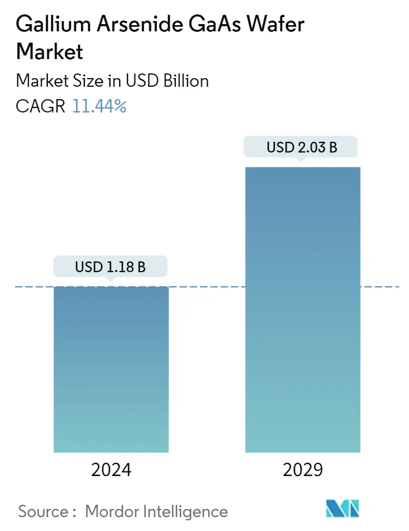
| Market Size (2024) | USD 1.18 Billion |
| Market Size (2029) | USD 2.03 Billion |
| CAGR (2024 - 2029) | 11.44 % |
| Fastest Growing Market | North America |
| Largest Market | Asia Pacific |
| Market Concentration | Low |
Major Players
*Disclaimer: Major Players sorted in no particular order |
Gallium Arsenide (GaAs) Wafer Market Analysis
The Gallium Arsenide GaAs Wafer Market size is estimated at USD 1.18 billion in 2024, and is expected to reach USD 2.03 billion by 2029, growing at a CAGR of 11.44% during the forecast period (2024-2029).
GaAs is mainly used is common in electronics, such as semiconductor manufacturing. The growing adoption of GaAs wafers in products such as LEDs, laser diodes, optoelectronic devices, and monolithic microwave integrated circuits is considered among the primary factors driving the growth of the studied market. The price of this compound being regulated creates more growth opportunities for gallium arsenide (GaAs) wafers manufacturers.
Gallium Arsenide or GaAs is a compound material made up of two elements. The semiconductor used to manufacture GaAs wafers is a direct bandgap semiconductor, meaning that electrons can pass through components much quicker without much interference, making them particularly useful in optoelectronic devices.
The increasing adoption of smartphones and computing devices and the growing penetration of light-emitting diodes (LEDs) in general lighting are significant growth drivers for this market. The advent of IoT has also been one of the major reasons responsible for the increasing market trend. The technology has also created a demand for high-frequency communication devices with GaAs-based ICs.
As a result, with several telecommunication companies expanding their communication infrastructure, the demand for GaAs wafers will increase, which will positively influence the growth of the studied market in the forthcoming years. Additionally, owing to its inherent features, the need for GaAs wafers across various end-user industries such as electronics, aerospace & defense, and communications is increasing, which, in turn, is also driving the demand for GaAs Wafers globally.
For instance, GaAs wafers are also a great choice for high-power outer space electronics and optical windows due to their wide direct bandgap material that resists radiation damage which is also predicted to offer profitable chances for market expansion and give rise to new market trends and use cases, including their higher adoption in electronic warfare systems, electric aircraft, and developments in broadband cellular network technology.
However, the price of GaAs wafers is among the major disadvantage, which explains its low utilization. To solve such issues, researchers have achieved new methods of manufacturing thin films of low-cost gallium arsenide to help create devices that would replace silicon to support the studied market's growth.
The global outbreak of the COVID-19 pandemic and the subsequent decisive government actions taken to curb the spread of the virus had a notable impact on the semiconductor sector, affecting the manufacture of semiconductor components and lowering customer demand, thereby impeding the global market's growth. However, higher exposure to digital technologies significantly enhanced the demand for advanced consumer electronic devices and supporting digital infrastructure, which positively influenced the growth of the studied market.
Gallium Arsenide (GaAs) Wafer Industry Segmentation
GaAs wafers find application in ultra-high radio frequency and fast electronic switching applications. GaAs Wafer is an III-V direct bandgap compound semiconductor used for multiple applications. It is a mixture of two elements: Gallium (Ga) and Arsenide (As) and has a zinc blend crystal structure. GaAs has a direct bandgap that allows the emission and absorption of light efficiently. It has exceptionally high electron mobility, which enables GaAs transistors to perform at frequencies exceeding 250 GHz and reduces the noise at which high frequencies tend to lessen the electrical signal disturbance in electronic circuits. GaAs wafers have a broad temperature functioning range or high thermal strength.
The Gallium Arsenide GaAs Wafer Market provides a detailed insight into the current market trends, demand across major end-user industries, and emerging future opportunities. The study segments the market by Application (Radio Frequency Electronics, Light Emitting Diodes, Photovoltaic Devices, Phototonic Devices) and Geography (United States, Taiwan, China, Japan, United Kingdom, Germany, and Rest of the World). The report offers the market size in value terms in USD for all the abovementioned segments.
| By Application | |
| Radio Frequency Electronics | |
| Light Emitting Diodes | |
| Photovoltaic Devices | |
| Phototonic Devices | |
| Other Applications |
| By Geography | |
| United States | |
| Taiwan | |
| China | |
| Japan | |
| United Kingdom | |
| Germany | |
| Rest of the World |
Gallium Arsenide GaAs Wafer Market Size Summary
The Gallium Arsenide (GaAs) Wafer Market is poised for significant growth, driven by its increasing application in electronics, particularly in semiconductor manufacturing. GaAs wafers are integral to the production of LEDs, laser diodes, optoelectronic devices, and monolithic microwave integrated circuits, which are essential for high-frequency communication devices. The compound's direct bandgap semiconductor properties enhance its utility in optoelectronic devices, making it a preferred choice for advanced technologies. The rising adoption of smartphones, computing devices, and IoT applications further propels the demand for GaAs wafers, as these devices require efficient and high-performance components. The market is also witnessing growth due to the expansion of telecommunication infrastructure and the need for high-power electronics in aerospace and defense applications.
Regionally, the Asia Pacific is a key player in the GaAs wafer market, with countries like China, Taiwan, Japan, and India driving demand through their burgeoning electronics industries and 5G network expansions. The region's focus on advanced technological devices and high-speed communication infrastructure supports the market's growth trajectory. China, in particular, benefits from government support and investments in domestic technology, fostering the development of the GaAs wafer market. The competitive landscape is characterized by a few dominant players investing in research and development to enhance product offerings and maintain market share. Innovations such as GaAs-based RF devices for wireless communication and advancements in microLED technology are expected to further stimulate market growth.
Gallium Arsenide GaAs Wafer Market Size - Table of Contents
-
1. MARKET INSIGHTS
-
1.1 Market Overview
-
1.2 Industry Attractiveness - Porter's Five Forces Analysis
-
1.2.1 Bargaining Power of Suppliers
-
1.2.2 Bargaining Power of Buyers
-
1.2.3 Threat of New Entrants
-
1.2.4 Threat of Substitute Products
-
1.2.5 Intensity of Competitive Rivalry
-
-
1.3 Technology Snapshot
-
1.3.1 Liquid Encapsulated Czochralski (LEC) Grown GaAs
-
1.3.2 Vertical Gradient Freeze (VGF) Grown GaAs
-
-
1.4 Assessment of the Impact of COVID-19 on the Market
-
-
2. MARKET SEGMENTATION
-
2.1 By Application
-
2.1.1 Radio Frequency Electronics
-
2.1.2 Light Emitting Diodes
-
2.1.3 Photovoltaic Devices
-
2.1.4 Phototonic Devices
-
2.1.5 Other Applications
-
-
2.2 By Geography
-
2.2.1 United States
-
2.2.2 Taiwan
-
2.2.3 China
-
2.2.4 Japan
-
2.2.5 United Kingdom
-
2.2.6 Germany
-
2.2.7 Rest of the World
-
-
Gallium Arsenide GaAs Wafer Market Size FAQs
How big is the Gallium Arsenide GaAs Wafer Market?
The Gallium Arsenide GaAs Wafer Market size is expected to reach USD 1.18 billion in 2024 and grow at a CAGR of 11.44% to reach USD 2.03 billion by 2029.
What is the current Gallium Arsenide GaAs Wafer Market size?
In 2024, the Gallium Arsenide GaAs Wafer Market size is expected to reach USD 1.18 billion.

