| Study Period | 2019 - 2030 |
| Base Year For Estimation | 2024 |
| Forecast Data Period | 2025 - 2030 |
| Market Size (2025) | USD 11.53 Billion |
| Market Size (2030) | USD 19.87 Billion |
| CAGR (2025 - 2030) | 11.50 % |
| Market Concentration | High |
Major Players*Disclaimer: Major Players sorted in no particular order |

EUV Lithography Market Analysis
The EUV Lithography Market size is estimated at USD 11.53 billion in 2025, and is expected to reach USD 19.87 billion by 2030, at a CAGR of 11.5% during the forecast period (2025-2030).
The extreme ultraviolet lithography industry is experiencing transformative advancements in semiconductor manufacturing equipment technology, driven by the increasing demand for smaller and more efficient chips. The technology utilizes light with a wavelength of just 13.5 nanometers, which represents a significant reduction compared to traditional deep ultraviolet photolithography techniques that use 193nm light. This technological leap has enabled semiconductor manufacturers to achieve unprecedented precision in chip fabrication, particularly for nodes at 7nm and below. The semiconductor industry's robust growth is evidenced by the Semiconductor Industry Association's report of worldwide chip sales reaching $555.9 billion in 2021, with a projected increase of 8.8% in 2022.
The industry is witnessing significant technological breakthroughs in manufacturing capabilities and efficiency. TSMC's EUV lithography tools have achieved remarkable production maturity, consistently delivering output power exceeding 250 watts for daily operations, while Intel's latest TWINSCAN EXE:5200 system demonstrates impressive capabilities with production volumes surpassing 200 wafers per hour. These advancements are crucial for meeting the escalating demand for sophisticated semiconductor applications in emerging technologies such as artificial intelligence, 5G communications, and autonomous vehicles.
Major industry players are aggressively pursuing technological leadership through strategic investments and innovation. TSMC is preparing to introduce its 2nm process products by 2024, while Intel has announced plans to implement its groundbreaking 18A (1.8nm) production technology by 2025. Samsung Electronics has set an ambitious goal to overtake TSMC's market position by 2030 through continued advancement in advanced lithography technology. These competitive dynamics are driving rapid innovation and development within the industry.
The evolution of chip architecture continues to yield impressive performance improvements. TSMC's latest 3nm technology demonstrates significant advantages over its predecessor, offering either a 10-15% increase in performance or a 25-30% reduction in power consumption compared to the 5nm process. This advancement is particularly crucial for next-generation applications in data centers, artificial intelligence processors, and mobile devices, where power efficiency and processing capabilities are paramount. The industry's focus on developing high-NA EUV lithography technology for 3nm nodes and beyond indicates a clear trajectory toward even more sophisticated manufacturing capabilities.
EUV Lithography Market Trends
The Technology Resulting in a Faster Output of Microchips Compared to Others
The extreme ultraviolet lithography (EUV) technology has emerged as a revolutionary solution for semiconductor manufacturing, enabling the production of increasingly sophisticated and miniaturized chips at unprecedented speeds. The technology utilizes light with a wavelength of 13.5 nanometers, which is more than 14 times shorter than traditional DUV light, allowing manufacturers to create more intricate patterns on silicon wafers with greater precision and efficiency. This advancement has enabled leading semiconductor companies to significantly accelerate their production capabilities, with TSMC planning to begin volume production of 3-nanometer products and further advancing toward 2-nanometer process products by 2024.
The superior capabilities of EUV technology are demonstrated through its ability to streamline the chip fabrication process by reducing the number of photolithography procedures required to produce more delicate circuits. For instance, ASML's latest-generation lithography equipment, the TWINSCAN NXE:3600D, supports EUV volume production at the 5 and 3 nm logic nodes while delivering more than 200 wafers per hour productivity. This technological breakthrough has enabled semiconductor manufacturers to meet the growing demand for advanced chips used in emerging technologies such as artificial intelligence, 5G communications, and autonomous vehicles, where processing power and energy efficiency are crucial requirements.
Understand The Key Trends Shaping This Market
Download PDF
Chipmakers Reducing the Manufacturing Process for Better Efficiency
Major semiconductor manufacturers are actively investing in EUV lithography technology to optimize their manufacturing processes and achieve better efficiency in chip production. TSMC has demonstrated significant progress in this direction by successfully implementing EUV technology in its manufacturing facilities, with their N7+ process offering 15% to 20% higher density and lower power consumption compared to the previous N7 process. This improvement in manufacturing efficiency has enabled chipmakers to produce more sophisticated processors while maintaining optimal energy consumption levels, directly addressing the industry's growing demand for high-performance computing solutions.
The drive for manufacturing efficiency has sparked substantial investments in research and development across the industry. Intel, for instance, has announced plans to invest over USD 20 billion in constructing two new leading-edge fabs in Ohio, incorporating advanced EUV lithography systems to enhance their manufacturing capabilities. Similarly, Samsung Electronics has unveiled a series of new microfabrication techniques, including FinFET, gate-all-around, and multi-bridge-channel FET, demonstrating the industry's commitment to improving manufacturing efficiency through innovative approaches. These advancements in manufacturing processes have enabled semiconductor companies to produce chips with higher transistor density while maintaining optimal production yields, ultimately contributing to more efficient and cost-effective semiconductor manufacturing equipment operations.
Segment Analysis: By Product Type
Masks Segment in EUV Lithography Market
The EUV masks segment continues to dominate the global EUV lithography market, commanding approximately 59% of the market share in 2024. EUV masks consist of 40-50 alternating layers of silicon and molybdenum on a substrate, resulting in a multi-layer stack that is 250-nm to 350-nm thick. These sophisticated components are crucial for semiconductor manufacturing as they contain the patterns of integrated circuits that need to be transferred to silicon wafers. The rising demand for semiconductors and increasing chip density are driving the growth of this segment. Product flatness remains one of the most critical characteristics of EUV photomasks, as even minor variations in the reflector plane can impact imaging efficiency and overall manufacturing quality.
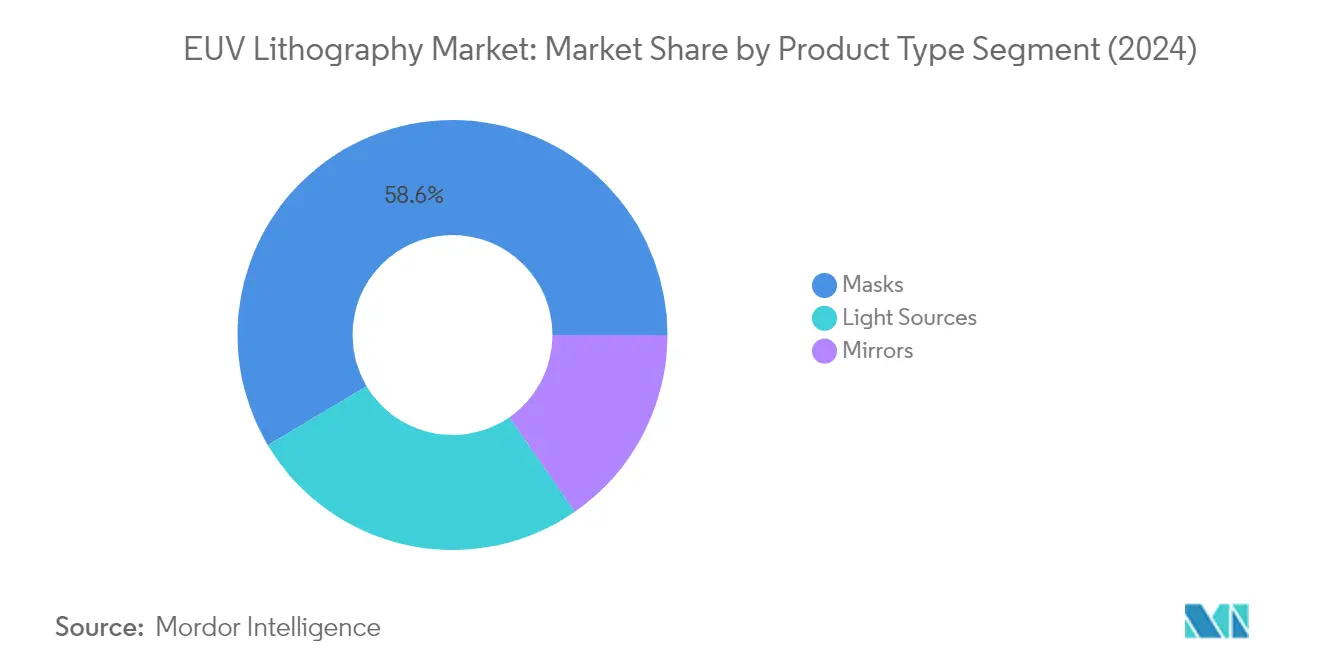
Light Sources Segment in EUV Lithography Market
The EUV light sources segment is projected to exhibit the highest growth rate of approximately 18% during the forecast period 2024-2029. This growth is primarily driven by continuous innovations in EUV light source technology, particularly in laser-produced plasma (LPP) techniques. The segment's expansion is supported by the increasing adoption of EUV lithography in semiconductor manufacturing, where light sources operating at a 13.5-nanometer wavelength enable the production of more sophisticated and miniaturized chips. The development of more efficient and reliable light sources, capable of delivering higher power outputs while maintaining stability, is expected to further accelerate segment growth.
Remaining Segments in Product Type Segmentation
The mirrors segment plays a vital role in the EUV lithography ecosystem, serving as crucial components for collecting and focusing EUV light within the lithography systems. These mirrors typically comprise over 50 pairs of molybdenum and silicon layers deposited on silicon wafers, with each layer being only a few nanometers thick. The technology requires ultra-smooth, multi-layer mirrors inside vacuum chambers, with each mirror containing over 100 precisely engineered layers chosen to maximize EUV light reflection. The continuous advancement in mirror technology and manufacturing processes remains essential for improving overall system performance and efficiency.
Segment Analysis: By Type
Foundry Segment in EUV Lithography Market
The Foundry segment has emerged as the dominant force in the global EUV lithography market, commanding approximately 59% of the market share in 2024. This substantial market presence is driven by the increasing adoption of extreme ultraviolet lithography technology by major foundries like Samsung, Taiwan Semiconductor Manufacturing Company (TSMC), and others for advanced chip manufacturing and wafer fabrication processes. The segment's dominance is further reinforced by significant investments in new manufacturing facilities and technology upgrades. For instance, TSMC's plans to dominate the global foundry market with its high-volume production of 3-nm products and Samsung Electronics' strategic initiatives to expand their EUV lithography capabilities have contributed significantly to the segment's growth. Additionally, the establishment of new semiconductor fabrication facilities and the increasing focus on developing more sophisticated chip designs for applications in 5G, artificial intelligence, and automotive sectors continue to drive the demand for EUV lithography in the foundry segment.
Integrated Device Manufacturers Segment in EUV Lithography Market
The Integrated Device Manufacturers (IDMs) segment plays a crucial role in the EUV lithography market, representing a significant portion of the industry. IDMs are increasingly focusing on enhancing their research and development activities to develop technically advanced semiconductor ICs, sensors, RFID circuits, and systems on chips. These manufacturers typically collaborate with semiconductor manufacturing equipment providers to increase their IC production capacities while emphasizing the enhancement of their IC manufacturing facilities. The segment's growth is further supported by strategic collaborations between IDMs and technology providers to develop next-generation EUV lithography systems. The increasing demand for micro-technologies, such as microprocessors, integrated chips, and other semiconductors, continues to fuel the demand for EUV lithographic systems among IDMs, positioning them as key stakeholders in the market's evolution.
EUV Lithography Market Geography Segment Analysis
EUV Lithography Market in Taiwan
Taiwan maintains its dominance in the global EUV lithography market, commanding approximately 31% of the market share in 2024, while also demonstrating the strongest growth trajectory at nearly 18% during 2024-2029. The country's leadership position is primarily driven by TSMC's aggressive expansion and continued investments in extreme ultraviolet lithography technology. Taiwan's semiconductor ecosystem benefits from strong government support and a well-established supply chain network. The country's focus on developing advanced manufacturing capabilities, particularly in sub-7nm processes, has attracted significant international partnerships and collaborations. Taiwan's semiconductor industry continues to push technological boundaries, with major investments in research and development facilities specifically focused on EUV lithography applications. The presence of world-class testing and packaging facilities further strengthens Taiwan's position as a crucial hub for advanced semiconductor manufacturing.
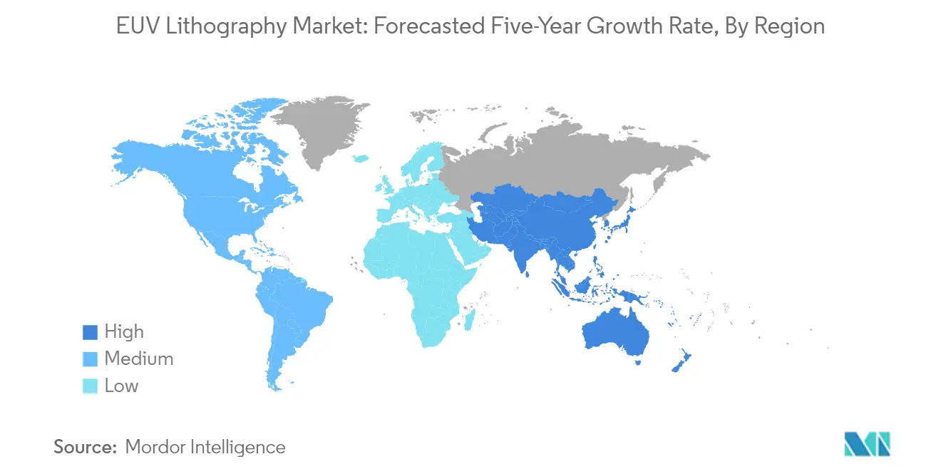
EUV Lithography Market in South Korea
South Korea has established itself as a pivotal player in the global EUV lithography landscape, driven primarily by Samsung Electronics' ambitious technological roadmap. The country's semiconductor industry benefits from a robust infrastructure and significant private sector investments in advanced manufacturing capabilities. South Korea's commitment to maintaining technological leadership is evident in its comprehensive approach to semiconductor manufacturing, encompassing research, development, and production. The country's semiconductor ecosystem is supported by strong government initiatives and policies aimed at maintaining its competitive edge in the global market. South Korean manufacturers have been particularly successful in implementing EUV technology for memory chip production, setting new industry standards for efficiency and innovation. The presence of advanced research facilities and a skilled workforce continues to attract international partnerships and collaborations, further strengthening South Korea's position in the EUV lithography market.
EUV Lithography Market in United States
The United States maintains a strategic position in the EUV lithography market, driven by its strong focus on technological innovation and research capabilities. The country's semiconductor industry benefits from substantial private sector investments and government support through various initiatives aimed at strengthening domestic chip manufacturing capabilities. American semiconductor companies have been particularly active in developing advanced node technologies and pushing the boundaries of EUV lithography applications. The presence of leading research institutions and a robust intellectual property framework continues to attract significant investments in semiconductor technology development. The United States' emphasis on creating a resilient semiconductor supply chain has led to increased investments in domestic manufacturing capabilities, particularly in advanced nodes utilizing EUV technology. The country's strong ecosystem of suppliers, researchers, and manufacturers continues to drive innovation in EUV lithography applications.
EUV Lithography Market in Other Countries
The EUV lithography market extends beyond the major players to include several other significant countries, each contributing uniquely to the global ecosystem. The Netherlands plays a crucial role as the home of ASML, the primary manufacturer of EUV lithography systems. Japan maintains its importance through its sophisticated semiconductor equipment and materials industry. China's growing semiconductor industry and ambitious plans for technological self-sufficiency are driving increased interest in EUV technology, although access remains limited by international trade restrictions. European countries, particularly Germany, are making strategic investments in semiconductor research and development, focusing on advanced manufacturing capabilities. These markets collectively contribute to the diverse and dynamic nature of the global EUV lithography landscape, each bringing unique strengths and capabilities to the industry.
Get Analysis on Important Geographic Markets
Download PDF
EUV Lithography Industry Overview
Top Companies in EUV Lithography Market
The EUV lithography market is characterized by companies focusing on continuous innovation in lithography systems and related technologies. Major players are investing heavily in research and development to advance their EUV lithography capabilities, particularly in developing next-generation high numerical aperture (High-NA) systems and improving existing technologies. Companies are demonstrating operational agility through strategic partnerships with research institutions, universities, and industry consortia to accelerate technological breakthroughs. Market leaders are expanding their manufacturing facilities globally while simultaneously strengthening their service networks to support the growing installed base of EUV systems. Strategic moves include vertical integration efforts to secure critical components and materials, as well as collaborations with semiconductor manufacturers to align technology roadmaps with future industry requirements.
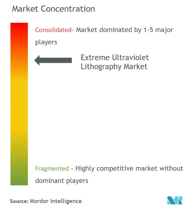
Consolidated Market with High Entry Barriers
The EUV lithography market exhibits a highly consolidated structure dominated by a few global technology conglomerates, with ASML Holdings maintaining a near-monopolistic position in EUV system manufacturing. The market's consolidation is reinforced by substantial technological barriers to entry, extensive intellectual property requirements, and the need for massive capital investments in research and development. The landscape is characterized by strong relationships between equipment manufacturers and major semiconductor foundries, creating a tightly integrated ecosystem that makes it challenging for new entrants to establish themselves.
The market has witnessed selective merger and acquisition activities, primarily focused on strengthening technological capabilities and securing supply chains rather than market consolidation. Major semiconductor manufacturers are making strategic investments in EUV technology providers to ensure access to critical technology and influence development roadmaps. Regional players, particularly in Asia, are attempting to develop domestic EUV capabilities through government-supported initiatives and industry collaborations, though significant technological gaps remain between established leaders and emerging contenders.
Innovation and Collaboration Drive Market Success
Success in the EUV lithography market requires a multi-faceted approach combining technological leadership, strong customer relationships, and operational excellence. Incumbent players must continue investing in next-generation technologies while simultaneously improving the cost-effectiveness and reliability of existing systems. Building and maintaining close partnerships with key semiconductor manufacturers, research institutions, and suppliers is crucial for aligning technology development with industry needs and ensuring stable supply chains. Companies must also focus on developing comprehensive service networks and technical support capabilities to maintain their competitive position.
For contenders seeking to gain ground, the path forward involves identifying and developing specialized niches within the broader EUV ecosystem, such as masks, light sources, or inspection systems. Success requires careful navigation of the concentrated customer base, dominated by major semiconductor manufacturers with stringent technical requirements and established supplier relationships. The regulatory environment, particularly regarding export controls and technology transfer restrictions, significantly impacts market dynamics and must be carefully considered in strategic planning. While substitution risk from alternative advanced lithography technologies exists, the industry's commitment to EUV for advanced node manufacturing suggests a stable long-term market for established players who can maintain technological leadership.
EUV Lithography Market Leaders
-
ASML Holding NV
-
Intel Corporation
-
Samsung Electronics Co. Ltd
-
Taiwan Semiconductor Manufacturing Company Limited
-
Toppan Photomasks Inc.
- *Disclaimer: Major Players sorted in no particular order
Need More Details on Market Players and Competiters?
Download PDF
EUV Lithography Market News
- January 2022: Intel has stated that it will begin employing ASML's High-NA Twinscan EXE scanners for high-volume manufacturing (HVM) in 2025, when the firm hopes to begin using its 18A (1.8 nm) production technique. With the first generation of extreme ultraviolet (EUV) lithography technology, Intel is obviously behind rivals TSMC and Samsung, but it intends to be the first to deploy the next-generation EUV tools.
- October 2021: Samsung Electronics said on Tuesday that it had launched the mass production of 14-nanometer (nm) DRAM, which will be produced using extreme ultraviolet (EUV) lithography. When compared to the prior Arf laser lithography, EUV lithography allows semiconductor makers to sketch finer circuit designs on the wafer.
EUV Lithography Market Report - Table of Contents
1. INTRODUCTION
- 1.1 Study Assumptions and Market Definition
- 1.2 Scope of the Study
2. RESEARCH METHODOLOGY
3. EXECUTIVE SUMMARY
4. MARKET INSIGHTS
- 4.1 Market Overview
- 4.2 Industry Value Chain Analysis
-
4.3 Industry Attractiveness - Porter's Five Forces Analysis
- 4.3.1 Bargaining Power of Suppliers
- 4.3.2 Bargaining Power of Buyers
- 4.3.3 Threat of New Entrants
- 4.3.4 Threat of Substitute Products
- 4.3.5 Intensity of Competitive Rivalry
- 4.4 Assessment of COVID-19 Impact on the Industry
5. MARKET DYNAMICS
-
5.1 Market Drivers
- 5.1.1 The technology resulting in a faster output of microchips compared to others
- 5.1.2 Chip makers reducing the manufacturing process for better efficiency
-
5.2 Market Restraints
- 5.2.1 High cost involved in replacing the existing Deep UV with EUV lasers
- 5.2.2 Monopoly existing within the market
- 5.3 Technology Snapshot
6. MARKET SEGMENTATION
-
6.1 Product Type
- 6.1.1 Light Sources
- 6.1.2 Mirrors
- 6.1.3 Masks
-
6.2 Type
- 6.2.1 Foundry
- 6.2.2 Integrated Device Manufacturers (IDMs)
-
6.3 Geography
- 6.3.1 South Korea
- 6.3.2 Taiwan
- 6.3.3 Others
7. COMPETITIVE LANDSCAPE
-
7.1 Company Profiles
- 7.1.1 ASML Holding NV
- 7.1.2 NTT Advanced Technology Corporation
- 7.1.3 Canon Inc.
- 7.1.4 Nikon Corporation
- 7.1.5 Intel Corporation
- 7.1.6 Taiwan Semiconductor Manufacturing Company Limited
- 7.1.7 Samsung Electronics Co. Ltd
- 7.1.8 Toppan Photomasks Inc.
- 7.1.9 Ushio, Inc.
- *List Not Exhaustive
8. INVESTMENT ANALYSIS
9. FUTURE OF THE MARKET
**Subject to Availability
You Can Purchase Parts Of This Report. Check Out Prices For Specific Sections
Get Price Break-up Now
EUV Lithography Industry Segmentation
Extreme Ultraviolet (EUV) lithography uses a EUV light of an extremely short wavelength of 13.5 nm. It allows exposure of delicate circuit patterns with a half-pitch below 20 nm that the conventional optical lithography cannot expose. Putting the technology into practical use requires a variety of element technologies, including the light source, optics, masks, photoresist, and lithography tools.
The Extreme Ultraviolet Lithography Market is segmented by Product Type (Light Sources, Mirrors, Masks), Ens-User (Foundry, Integrated Device Manufacturers), and Geography.
| Product Type | Light Sources |
| Mirrors | |
| Masks | |
| Type | Foundry |
| Integrated Device Manufacturers (IDMs) | |
| Geography | South Korea |
| Taiwan | |
| Others |
Need A Different Region or Segment?
Customize Now
EUV Lithography Market Research FAQs
How big is the EUV Lithography Market?
The EUV Lithography Market size is expected to reach USD 11.53 billion in 2025 and grow at a CAGR of 11.5% to reach USD 19.87 billion by 2030.
What is the current EUV Lithography Market size?
In 2025, the EUV Lithography Market size is expected to reach USD 11.53 billion.
Who are the key players in EUV Lithography Market?
ASML Holding NV, Intel Corporation, Samsung Electronics Co. Ltd, Taiwan Semiconductor Manufacturing Company Limited and Toppan Photomasks Inc. are the major companies operating in the EUV Lithography Market.
What years does this EUV Lithography Market cover, and what was the market size in 2024?
In 2024, the EUV Lithography Market size was estimated at USD 10.20 billion. The report covers the EUV Lithography Market historical market size for years: 2019, 2020, 2021, 2022, 2023 and 2024. The report also forecasts the EUV Lithography Market size for years: 2025, 2026, 2027, 2028, 2029 and 2030.
Our Best Selling Reports
EUV Lithography Market Research
Mordor Intelligence offers a comprehensive analysis of the extreme ultraviolet lithography industry. We leverage deep expertise in semiconductor manufacturing equipment and advanced processing technologies. Our extensive research covers the complete spectrum of photolithography technologies, ranging from deep ultraviolet lithography to cutting-edge EUV lithography solutions. The report provides detailed insights into semiconductor process equipment. It includes information on EUV scanner technologies, EUV mask developments, and EUV light source innovations. This offers stakeholders a complete understanding of advancements in semiconductor lithography.
Our detailed analysis benefits stakeholders across the semiconductor patterning ecosystem, from manufacturers to investors. It includes in-depth coverage of advanced lithography technologies, such as nanolithography and wafer lithography processes. The report, available as an easy-to-download PDF, examines crucial components like EUV resist materials and DUV lithography systems. It also provides comprehensive insights into semiconductor manufacturing equipment market dynamics. This thorough analysis of EUV photolithography technologies enables informed decision-making for industry participants. It is supported by extensive data on leading extreme ultraviolet lithography companies and their technological innovations.