Epitaxy Equipment Market Size and Share
Market Overview
| Study Period | 2020 - 2031 |
|---|---|
| Market Size (2026) | USD 6.41 Billion |
| Market Size (2031) | USD 11.5 Billion |
| Growth Rate (2026 - 2031) | 12.43% CAGR |
| Fastest Growing Market | Asia Pacific |
| Largest Market | North America |
| Market Concentration | Medium |
Major Players *Disclaimer: Major Players sorted in no particular order Image © Mordor Intelligence. Reuse requires attribution under CC BY 4.0. | |
Epitaxy Equipment Market Analysis by Mordor Intelligence
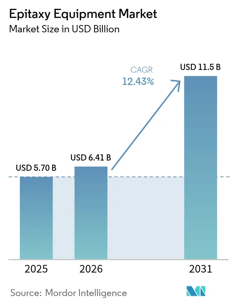
The epitaxy equipment market size was valued at USD 5.7 billion in 2025 and estimated to grow from USD 6.41 billion in 2026 to reach USD 11.5 billion by 2031, at a CAGR of 12.43% during the forecast period (2026-2031). Demand increases as compound semiconductor manufacturers scale capacity for electric-vehicle power modules, 5G base-station front-end chips, and high-brightness LED backlighting. Precision epitaxial layers on silicon-carbide and gallium-nitride substrates now dictate performance in high-power and high-frequency devices, encouraging integrated-device manufacturers to pivot capital budgets away from legacy silicon tools. U.S. CHIPS Act allocations exceeding USD 300 million dedicated to epitaxy lines confirm the process as a sovereignty priority. Equipment suppliers answer with larger-wafer reactors, tighter process-control software, and flexible multi-material chambers, preserving yield while lowering cost per die. However, lengthy tool-qualification cycles and precursor price swings continue to temper near-term shipment rhythms even as long-term growth fundamentals remain intact.
Key Report Takeaways
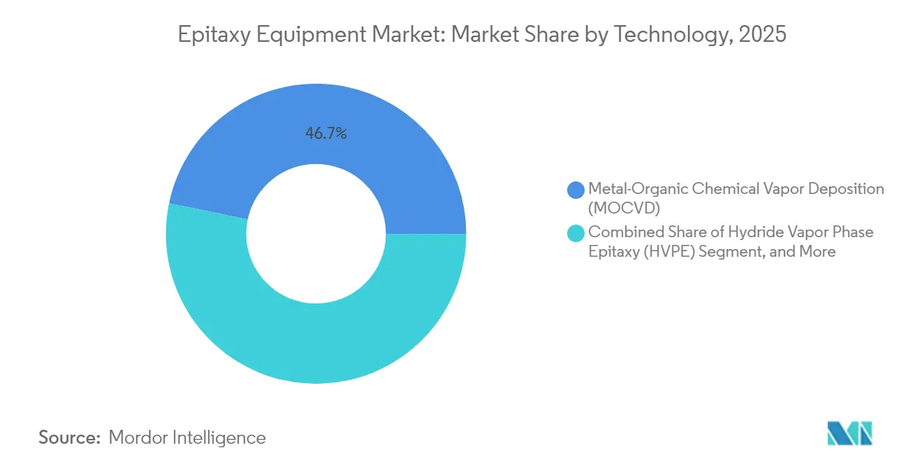
- By technology, metal-organic chemical vapor deposition held 46.73% of the epitaxy equipment market share in 2025.
- Remote-plasma CVD is forecast to expand at a 13.35% CAGR through 2031, the quickest among deposition technologies.
- By application, compound-semiconductor devices captured 52.10% revenue share in 2025; wide-bandgap materials are advancing at a 13.52% CAGR to 2031.
- By material, silicon carbide accounted for 71.05% of the epitaxy equipment market size in 2025, while gallium-nitride tools are growing at a 15.65% CAGR through 2031.
- By region, North America commanded 43.25% revenue in 2025; Asia-Pacific records the fastest CAGR of 15.22% to 2031.
Note: Market size and forecast figures in this report are generated using Mordor Intelligence’s proprietary estimation framework, updated with the latest available data and insights as of 2026.
Global Epitaxy Equipment Market Trends and Insights
Drivers Impact Analysis*
| Driver | (~) % Impact on CAGR Forecast | Geographic Relevance | Impact Timeline |
|---|---|---|---|
| Increasing demand for high-brightness LEDs | +2.10% | APAC core, spill-over to North America | Medium term (2-4 years) |
| Rapid electrification of powertrains in EVs | +2.80% | Global, with early gains in North America, Europe, China | Long term (≥ 4 years) |
| Expansion of 5G/6G compound-semiconductor front-end modules | +1.80% | Global, concentrated in APAC and North America | Medium term (2-4 years) |
| Government incentives for SiC/GaN capacity build-out | +2.20% | North America & EU, selective APAC markets | Short term (≤ 2 years) |
| Adoption of gallium-oxide (β-Ga₂O₃) devices | +0.80% | Global R&D centers, early commercial in Japan, US | Long term (≥ 4 years) |
| Transition to 8- and 12-inch GaN-on-Si epitaxy lines | +1.50% | Global, led by advanced fabs in Taiwan, Korea, US | Medium term (2-4 years) |
| Source: Mordor Intelligence | |||
Increasing Demand for High-Brightness LEDs
MicroLED and mini-LED adoption in premium displays and automotive lighting causes LED makers such as San’an Optoelectronics to book multi-system MOCVD orders. Throughput upgrades must coincide with lower defect density across 6- and 8-inch wafers, keeping Veeco’s Lumina platform backlog elevated.[1]Compound Semiconductor Staff, “PlayNitride Selects Veeco MOCVD System,” compoundsemiconductor.net Automotive daytime-running lamps and adaptive-beam headlamps also require higher luminous flux, which in turn pushes epitaxy specifications for GaN layer uniformity. These combined forces translate into a predictable equipment-replacement cycle every three to four years, fortifying mid-term shipment trajectories.
Rapid Electrification of Powertrains in EVs
Automakers migrate to 800 V architectures, accelerating silicon-carbide MOSFET and diode uptake that demands epitaxial layers grown at ≥1,600 °C. Tokyo Electron’s high-temperature CVD tool bookings rose in tandem with Bosch securing USD 225 million in CHIPS Act grants for Alabama SiC lines.[2]U.S. Department of Commerce, “CHIPS Act Funding Announcements,” commerce.gov The move from 150 mm to 200 mm SiC substrates compels both new-tool investments and retrofit kits across global fabs. Because power-module yields are hypersensitive to micropipe density and doping drift, device makers award purchase orders only after months of process-recipe co-engineering, extending revenue recognition yet building an entrenched installed base.
Expansion of 5G/6G Compound-Semiconductor Front-End Modules
Gallium-nitride high-electron-mobility transistors outperform LDMOS in 3–8 GHz 5G bands, prompting base-station OEMs to expand GaN-on-SiC epitaxy lines. Research alliances led by Imec validate GaN and indium-phosphide scaling for 140 GHz 6G concepts, keeping university and pilot-fab tools active.[3]IEEE Authors, “MOCVD Reactor Optimization Research,” ieeexplore.ieee.org Mobile handset suppliers mirror infrastructure trends by qualifying GaN RF switches to curb heat and extend battery life. Combined, these infrastructure and consumer rollouts widen the demand funnel for premium-grade epitaxy systems over the medium term.
Government Incentives for SiC/GaN Capacity Build-Out
Public funding under the U.S. CHIPS Act and the European Chips Act covers a share of capex for domestic epitaxy and substrate plants. Coherent won USD 79 million to scale SiC epitaxy in Texas, while IntelliEPI received USD 10.3 million for military-grade MBE R&D.[4]U.S. Department of Commerce, “CHIPS Act Funding Announcements,” commerce.gov Subsidies mandate local supply commitments, tilting near-term orders toward home-region tool suppliers and accelerating lead times for qualifying new reactor designs. The incentive wave compresses a five-year capacity pipeline into a two-year window, creating backlog peaks but also heightening competition for skilled process engineers.
Restraints Impact Analysis*
| Restraint | (~) % Impact on CAGR Forecast | Geographic Relevance | Impact Timeline |
|---|---|---|---|
| Complexities associated with reactor design | -1.90% | Global, affecting all major equipment suppliers | Medium term (2-4 years) |
| Volatile prices and supply of specialty precursors | -1.10% | Global, with acute impact in Asia-Pacific | Short term (≤ 2 years) |
| Lengthy tool qualification cycles at IDMs and foundries | -0.80% | Global, concentrated at tier-1 semiconductor fabs | Medium term (2-4 years) |
| High capex for next-gen high-temperature reactors | -0.60% | Global, affecting capacity expansion decisions | Long term (≥ 4 years) |
| Source: Mordor Intelligence | |||
Complexities Associated With Reactor Design
As fabs request dual-material or 300 mm chambers, computational-fluid-dynamics models must reconcile laminar gas flow with sharp temperature gradients, lengthening R&D cycles. Suppliers therefore integrate multi-zone heaters, motorized injector plenums, and in-situ spectroscopic ellipsometry, driving up bill-of-materials and software validation costs. These engineering hurdles defer revenue and raise the entry barrier for latecomers.
Volatile Prices and Supply of Specialty Precursors
Metal-organic trimethylgallium and trichlorosilane depend on a handful of purification plants; any outage ripples through MOCVD throughput within a month. The high-purity precursor market grew with a high CAGR in 2024 but remains concentrated in fewer than ten global vendors. Supply shocks force LED fabs to idle reactors, cutting utilization and delaying new-tool ROI. To mitigate risk, device makers push for multi-source qualification, extending procurement cycles and inflating raw-material buffers, a cost that indirectly weighs on tool investments.
*Our forecasts treat driver/restraint impacts as directional, not additive. The impact forecasts reflect baseline growth, mix effects, and variable interactions.
Segment Analysis
By Technology: MOCVD Retains Scale Advantages While RPCVD Surges
Metal-organic chemical vapor deposition occupied 46.73% of the epitaxy equipment market share in 2025 on the back of its entrenched position in LED and GaN power devices. The segment’s scale enables incremental wafer-size increases without catastrophic redesign, sustaining repeat orders. Remote-plasma CVD, though, is projected to post a 13.35% CAGR as lower-temperature processing opens doors to fragile substrates and tighter interface control. The epitaxy equipment market size for RPCVD tools is expected to reach USD 1.59 billion by 2031. MBE and hydride vapor-phase epitaxy remain niche, favored for ultra-pure heterostructures and thick GaN substrates, respectively, while HT-CVD dominates SiC layers exceeding 20 µm thickness. Across all platforms, suppliers position multi-material flexibility as a hedge against future technology nodes.
A second competitive angle revolves around advanced process-control stacks. Tier-one fabs increasingly insist on closed-loop emissivity-corrected pyrometry and machine-learning fault detection, features most readily retrofitted to MOCVD and RPCVD architectures. Consequently, average selling prices rise faster than unit volumes, cushioning margins even as entry-level Chinese tools crowd the LED subsegment. Open-platform software ecosystems emerge as another differentiator, enabling fabs to port recipes across vendor hardware and thus shorten qualification cycles.


By Application: Compound Semiconductors Lead, Wide-Bandgap Demand Accelerates
Compound-semiconductor device manufacturing captured 52.10% of 2025 revenue, driven by RF amplifiers, LiDAR VCSELs, and photonics transceivers. Yet the fastest uplift stems from wide-bandgap materials used in electric-vehicle inverters and telecom power supplies, advancing 13.52% annually. The epitaxy equipment market size for wide-bandgap applications stood at USD 2.28 billion in 2025 and could surpass USD 4.88 billion by 2031. Photonics lines, especially indium-phosphide PICs, benefit from hyperscale data-center optics, evidenced by Coherent tripling InP output at its Texas site. MEMS foundries, though smaller, rely on custom epitaxial stacks for pressure sensors and RF filters, carving a steady yet specialized equipment niche.
The diversity of end-use cases forces equipment makers to supply modular reactors configurable between SiC, GaN, and InP within the same fab footprint. Such adaptability protects capex budgets from sudden demand shifts. Concurrently, partnerships between tool vendors and chemical suppliers aim to co-optimize precursor flow dynamics, improving film stoichiometry and unlocking new device architectures such as GaN vertical transistors.
By Wafer Size: Migration to 300 mm Gains Traction
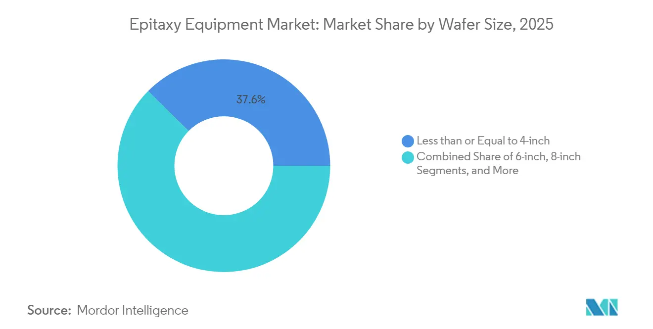
Wafers of Less than or Equal to 4-inch diameter still represent 37.62% of units because universities and pilot lines rely on small substrates for exotic compounds. Nevertheless, 12-inch systems exhibit the highest 14.92% CAGR, propelled by microLED, GaN power IC, and advanced RF programs. Line-item quotations show that a single 300 mm GaN MOCVD reactor can replace three 150 mm tools, cutting fab footprint by 30%. The epitaxy equipment market size allocated to 12-inch tools could top USD 3.22 billion by 2031. Intermediate 6- and 8-inch nodes serve as stepping-stones for SiC and InP, balancing yield risk with cost savings.
Engineering hurdles revolve around center-to-edge uniformity. Suppliers combat radial temperature drift with multi-zone susceptor heaters and rotating showerheads. Demand for in-situ metrology rises accordingly: real-time PL mapping and pyrometric feedback now ship standard on most 300 mm installations. Such features shorten recipe development, enhancing the value proposition despite higher list prices.
By Material: SiC Dominance Meets GaN Momentum
Silicon-carbide commanded 71.05% of revenue in 2025 thanks to automotive and renewable-energy inverters. Yet gallium-nitride tool revenue is growing 15.65% annually, poised to reshape shipment mix by 2031. The epitaxy equipment market share split will likely compress as GaN power ICs move from 650 V to 1,200 V classes, requiring thicker epitaxial layers and therefore more sophisticated reactors. III-V arsenides and phosphides remain essential for optoelectronics, while research into β-Ga₂O₃ attracts grant-funded prototype tools aimed at ≥3.3 kV devices. Process recipes diverge markedly: SiC favors hot-wall graphite reactors and high partial pressures of silane, whereas GaN leans on cold-wall metal-organic flow and ammonia overpressure, compelling OEMs to maintain distinct product lines.
Material-specific subsidy programs amplify the split. U.S. and German car OEMs invest directly in SiC lines to secure traction-inverter supply, whereas telecom players co-finance GaN RF capacity. As both camps scale, metrology packages fine-tune oxygen and carbon contamination levels to below 1×10¹⁵ cm⁻³, an imperative for defect-free drift zones.
Geography Analysis
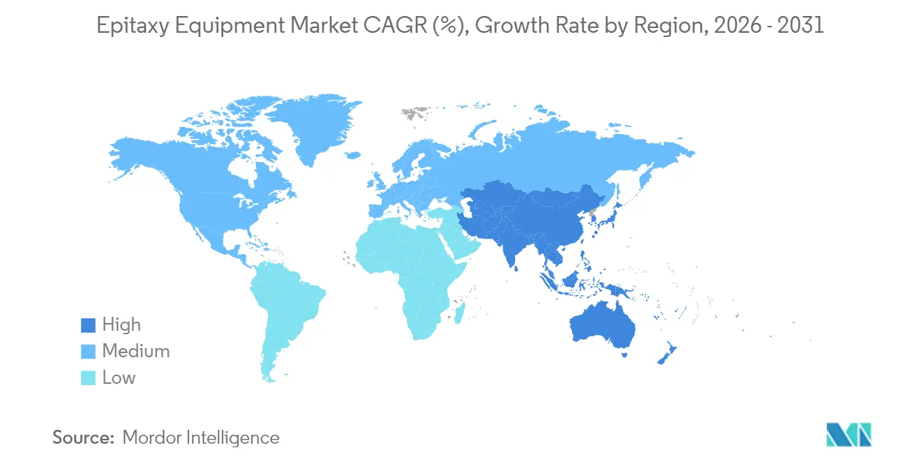
North America preserved a 43.25% revenue share in 2025, supported by dense clusters in Texas, Arizona, and upstate New York. CHIPS Act disbursements flow to both greenfield fabs and brownfield upgrades, anchoring long-term demand for domestic epitaxy capacity. Coherent’s Sherman campus, for instance, tripled InP device output to meet AI optical-link demand. Local sourcing rules embedded in government contracts tilt procurement toward resident suppliers, bolstering order pipelines even as exchange-rate swings temper export competitiveness.
Asia-Pacific represents the fastest-growing theater with a 15.22% CAGR through 2031. Chinese LED houses such as HC SemiTek accumulate MOCVD install bases that already exceed 2,500 reactors, driving unit-volume leadership. Simultaneously, South Korean memory giants invest in compound-semiconductor roadmaps for CXL photonics and HBM power delivery, widening the regional addressable market. Tokyo Electron’s net sales climb to YEN 654.5 billion in Q1 2025 underscores the pull-through effect on upstream tool vendors.
Europe concentrates on automotive electrification and resilient aerospace supply chains. Programs under the European Chips Act channel subsidies to SiC epi fabs in Germany and Sweden, while French institutes pilot 200 mm GaN-on-Si lines for radar and satellite payloads. Local environmental regulations expedite adoption of low-global-warming-potential process gases, prompting European fabs to specify upgraded abatement modules. Although the region trails in unit volumes, it excels in high-margin specialty tools and research-grade MBE systems tailored for quantum-computing materials.

Regulatory Landscape
Export controls and dual-use rules remain the main regulatory touchpoints for epitaxy equipment shipments, especially for advanced compound-semiconductor and leading-edge manufacturing use cases. The European Commission updated the EU Dual-Use List via Commission Delegated Regulation (EU) 2025/2003 (effective from November 2025), adding controls that explicitly cover categories of advanced semiconductor manufacturing equipment, including epitaxial deposition tools. For cross-border deliveries, this expands licensing and classification workload.
In Japan, METI tightened oversight around semiconductor-related exports and technology transfers, including a prior notification system implemented in December 2024 for overseas technology transfers in key semiconductor fields and a Cabinet Decision in March 2025 to amend export-control orders. In the United States, the Department of Commerce (BIS) continues to refine controls on advanced computing and semiconductor manufacturing items related to the PRC, sustaining a compliance environment where US, EU, and Japan requirements diverge and push region-specific screening, end-use checks, and documentation for tool makers and their customers.
Value Chain Analysis
The epitaxy equipment value chain starts with upstream precision components and materials, including high-temperature heaters and susceptors (often graphite-based for SiC), vacuum hardware, RF or plasma subsystems for RPCVD variants, gas delivery and abatement modules, and specialty electronics and software stacks for closed-loop process control. These inputs feed into tool OEM design, reactor integration, factory acceptance testing, and field installation, followed by recipe co-development and long qualification cycles at IDMs, foundries, and LED makers, where yield sensitivity makes process-transfer services a material part of delivered value.
Downstream demand is pulled by device manufacturers scaling SiC and GaN power, RF, and optoelectronic production, as well as photonics, notably InP, where tool orders often bundle epitaxy with complementary steps such as etch. Industry structure also reflects selective vertical integration and portfolio consolidation, with ASM International strengthening its silicon-carbide epitaxy position through the acquisition of LPE S.p.A., while suppliers such as Veeco and Aixtron emphasize platform families (for example, TurboDisc-based MOCVD for compound semiconductors) and recurring service, spares, and upgrade revenue from large installed bases.
Competitive Landscape
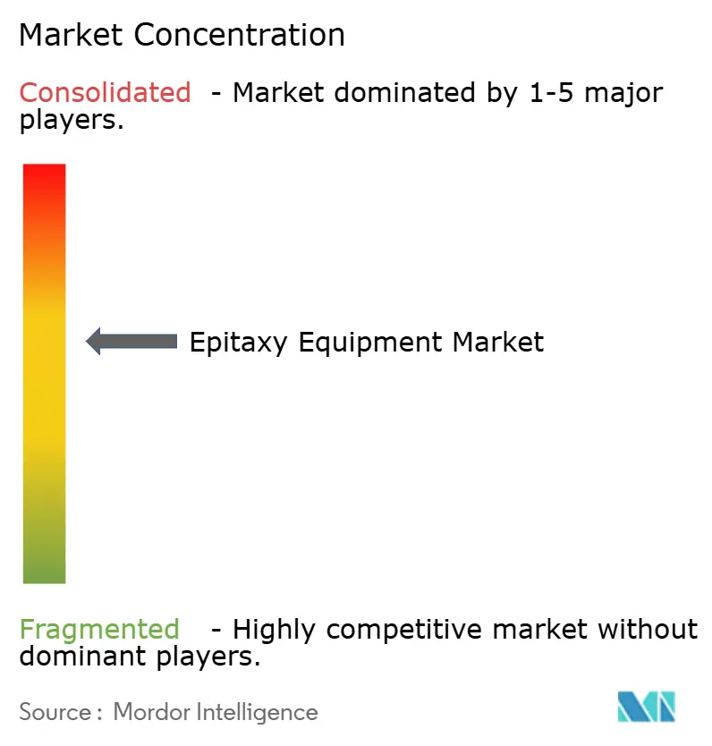
Incumbent suppliers Tokyo Electron, Aixtron, and Applied Materials jointly delivered over half of 2024 shipment value, reflecting moderate concentration. Each differentiates via proprietary showerhead geometries, multi-zone heaters, and recipe-transfer software that lock customers into upgrade paths. Average selling price resilience offsets cyclical volume dips, preserving gross margins above 40%. Meanwhile, Veeco’s focus on 300 mm GaN platforms secures strategic wins at display and power startups, raising competitive intensity in the premium tier.
Emerging Chinese manufacturers leverage cost advantages to penetrate first-generation LED lines but struggle to match the uniformity specifications demanded by SiC and high-frequency GaN fabs. Some Western IDMs impose export-control vetting, effectively gating high-temperature reactor adoption outside OECD supply chains. Consequently, market entrants often pursue joint ventures with established brands to gain process IP and customer trust.
Technology roadmaps gravitate toward closed-loop machine learning analytics that predict particle excursions before yield hits occur. Aixtron and Applied Materials pilot edge AI modules that correlate real-time chemiluminescence signals with wafer-level defects, promising up to 3% yield uplift. Intellectual-property litigation occasionally surfaces around plasma-source designs, indicating intangible assets as a core battleground. Despite these skirmishes, supply-chain resilience efforts push customers to adopt multi-vendor strategies, sustaining healthy rivalry without triggering destructive price wars.
Epitaxy Equipment Industry Leaders
Aixtron SE
Applied Materials, Inc.
Tokyo Electron Limited
Veeco Instruments Inc.
LPE S.p.A.
- *Disclaimer: Major Players sorted in no particular order

Market Opportunities and Future Outlook
Whitespace is forming around InP-based photonics scale-up for AI-driven optical interconnects, and this is translating into larger, bundled purchase orders that combine epitaxy with adjacent process equipment. Veeco disclosed in May 2026 that it received more than USD 250 million in equipment orders (including Lumina MOCVD, Spector ion beam deposition, and WaferEtch systems) to support InP laser manufacturing for silicon photonics. It also suggests that capacity additions are increasingly being executed as integrated tool sets rather than standalone epitaxy buys.
Another opportunity centers on accelerating in-house GaN power device manufacturing expansions that require repeatable, high-volume epitaxy on larger wafer formats and tighter uniformity control. AIXTRON confirmed in May 2026 that it supplied multiple Planetary G5+C systems to Renesas for high-volume GaN manufacturing expansion, and in June 2026 Rohm selected AIXTRON G10-GaN systems for in-house 8-inch GaN epitaxy at its Hamamatsu site. Upstream substrate investments reinforce this build-out cycle, with JX Advanced Metals announcing in June 2026 a plan of up to JPY 120 billion over four years to expand InP substrate production capacity, and Sumitomo Electric disclosing in July 2026 an approximately JPY 18 billion upgrade to InP substrate production lines at its Itami Works.
Recent Industry Developments
- June 2026: Applied Materials introduced an enhanced Centura Prime Epi system aimed at bringing logic-class epitaxy capability into DRAM manufacturing. The platform focus on power efficiency and higher tool density supports memory makers pursuing AI-driven architectures that depend on tighter device control and integration.
- May 2026: AIXTRON supplied multiple Planetary G5+C GaN MOCVD systems to Renesas for high-volume manufacturing expansion of GaN power devices. The deliveries highlight continued capex for wide-bandgap production and reinforce demand for repeatable, high-throughput epitaxy in power semiconductor lines.
- December 2024: Coherent received USD 33 million in CHIPS Act funding to expand indium phosphide (InP) capacity. The award strengthened domestic photonics manufacturing investment, which supports demand for specialized epitaxy process steps and associated equipment in North America.


Research Methodology Framework and Report Scope
Market Definition and Coverage
This market covers tools used to grow epitaxial layers on wafers for semiconductor and compound semiconductor manufacturing, including reactors and key supporting modules sold as part of the equipment sale. We size the market in value terms using equipment revenues linked to epitaxy process steps.
Scope exclusions: We exclude upstream wafer materials, metal-organic precursors and gases, spare parts not sold as part of the original tool package, and in-house labor costs at fabs.
Segmentation Overview
- By Technology
- Metal-Organic Chemical Vapor Deposition (MOCVD)
- Hydride Vapor Phase Epitaxy (HVPE)
- High-Temperature Chemical Vapor Deposition (HT-CVD)
- Molecular Beam Epitaxy (MBE)
- Remote-Plasma CVD (RPCVD)
- By Application
- Photonics
- Semiconductors
- Wide-Bandgap Materials
- Micro-Electro-Mechanical Systems (MEMS)
- Others
- By Wafer Size
- Less than or Equal to 4-inch
- 6-inch
- 8-inch
- 12-inch
- Greater than 12-inch
- By Material
- III-V (GaAs, InP)
- GaN
- SiC
- Others
- By Geography
- North America
- United States
- Canada
- Mexico
- South America
- Brazil
- Argentina
- Rest of South America
- Europe
- Germany
- United Kingdom
- France
- Italy
- Spain
- Russia
- Rest of Europe
- Asia-Pacific
- China
- Japan
- India
- South Korea
- South-East Asia
- Rest of Asia-Pacific
- Middle East and Africa
- Middle East
- Saudi Arabia
- United Arab Emirates
- Turkey
- Rest of Middle East
- Africa
- South Africa
- Nigeria
- Rest of Africa
- Middle East
- North America
Data Sources, Market Sizing, and Validation
Desk Research
Desk work starts by building the demand context for epitaxy tools, then narrows it to the value of purchasable equipment. Public sources such as SEMI publications, U.S. International Trade Commission trade statistics, UN Comtrade, World Semiconductor Trade Statistics releases, and OECD manufacturing indicators are used to sanity check cycle timing and regional investment momentum.
We also review company filings, earnings call transcripts, and investor presentations to map product exposure to epitaxy and to understand how shipment timing relates to revenue recognition. Patent databases are used to track process shifts, for example GaN and SiC related reactor designs, which then informs what suppliers realistically bring to qualification and adoption during the forecast window. The sources listed here are illustrative, and many other public references were also used for data collection, validation, and clarification.
Primary Interviews and Surveys
Primary work is used to stress test tool demand assumptions with people who are directly involved in the buying decision, including equipment suppliers, component ecosystems, and fab-level process and procurement roles. Since this is a global market, discussions are spread across major producing and consuming regions so that expansion plans, qualification timelines, and ASP expectations can be compared and aligned to one consistent model.
Distribution of primary research fieldwork respondents
| Company type | Respondent position | Region |
|---|---|---|
| Top tier: 26% | CXOs: 19% | APAC: 47% |
| Mid tier: 55% | Functional/Unit leaders: 30% | EMEA: 29% |
| Smaller Players: 19% | Managers: 51% | Americas: 24% |
Market-Sizing & Forecasting
Our sizing starts with a top-down build where semiconductor and compound semiconductor capex signals are reconstructed into an epitaxy-specific demand pool using adoption and process intensity checks. Totals are then corroborated with selective bottom-up approximations, such as sampled tool ASPs multiplied by expected shipment volumes, plus channel checks on booking patterns, which are used to adjust the final market value.
Key inputs in the model include wafer size migration (for example, 150 mm to 200 mm in some compound lines), expansion plans for GaN and SiC device capacity, typical tool qualification and ramp timelines, mix shifts between MOCVD, MBE, and related technologies, and the share of new fabs versus brownfield expansions. When the data is patchy by region, gaps are handled by applying conservative penetration ranges agreed in interviews and cross-checked against recent fab announcements and trade flows.
Forecasting relies on scenario analysis supported by an exponential smoothing view of near-term cycle swings, because order timing in capital equipment can move quickly while qualification slows actual tool placements. Assumptions on utilization, expansion pacing, and pricing progression are refreshed during the build, and the final path is reviewed against what respondents describe as realistic procurement timing.
Data Validation & Update Cycle
Validation is done through triangulation across independent signals, where the modeled market is compared with capex direction, trade indicators, and publicly visible fab build outs before sign-off. If a large variance shows up, the driver is traced back to the input layer, then the assumption is either re-checked in sources or re-confirmed through re-contact with an expert to verify the interpretation.
A multi-step analyst review is followed so that the calculation logic, currency handling, and year mapping remain consistent throughout the workbook. Reports are refreshed annually, and interim updates are made when material events occur, such as sudden export controls, a major fab delay, or a sharp demand shift in power or RF devices. Before delivery, a fresh pass is completed so clients receive the latest updated view.
Mordor Intelligence's Epitaxy Equipment Market Size Measured Against Other Published Estimates
Published market sizes for epitaxy equipment can vary even when they appear to describe the same space, because the boundaries and timing assumptions are not always aligned. Differences often come from what is counted as equipment value versus materials, how the base year is picked, and whether the forecast reflects a cycle peak, a mid-cycle year, or a more normalized run rate.
By tracking wafer-size transitions, device-led capacity adds (GaN and SiC), and capex-to-tool conversion timing, Mordor Intelligence keeps the estimate tied to tool shipments and qualification reality rather than broad semiconductor spending totals. Some estimates fold adjacent items like precursors, spares, or wider deposition tools into the same bucket, and a few also anchor the starting year earlier in the downcycle, which can pull the current value lower even if the long-term growth narrative appears similar.
Benchmark comparison
| Source | Market Size | Gaps in Research Methodology |
|---|---|---|
| Mordor Intelligence | USD 6.41 B (2026) | |
| Global Research Publisher A | USD 4.76 B (2024) | Uses an earlier base year and a longer horizon, and the cycle point chosen appears more conservative for equipment orders, which can compress the near-term market value compared to a capex-to-shipments timing build. |
| Industry Research Publisher B | USD 4.33 B (2025) | The scope description is broader and less explicit on tool-only boundaries, and it likely applies slower ASP and adoption progression for wide-bandgap expansions, which reduces the starting market size. |
The table shows that the spread is mainly explained by base-year selection and what is kept inside the equipment definition. When the scope is kept tool-focused and the timing from capex decisions to qualified shipments is made explicit, the resulting number becomes easier to audit and repeat from one update to the next using the same input checks.


Key Questions Answered in the Report
What revenue does the epitaxy equipment market generate in 2026?
The epitaxy equipment market size stands at USD 6.41 billion in 2026.
Which technology currently leads unit shipments?
Metal-organic chemical vapor deposition commands 46.73% shipment share because of its entrenched use in LED and GaN devices.
Why are SiC tools seeing strong demand from automakers?
Transition to 800 V electric-vehicle architectures requires low-defect SiC epitaxial layers for inverters and onboard chargers.
Which region is growing fastest for new reactor installations?
Asia-Pacific records a 15.22% CAGR through 2031, fueled by Chinese LED expansion and Korean memory investments.
How will 12-inch wafer tools impact cost structure?
A single 300 mm reactor can replace three 150 mm tools, reducing fab footprint by 30% and lowering cost per die.
What is the biggest supply-chain risk for epitaxy production?
Limited sources of high-purity metal-organic precursors create price volatility and potential reactor idle time.
Page last updated on: