Embedded Die Packaging Market Size
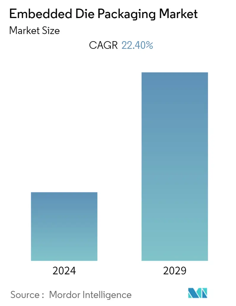
| Study Period | 2019 - 2029 |
| Base Year For Estimation | 2023 |
| CAGR | 22.40 % |
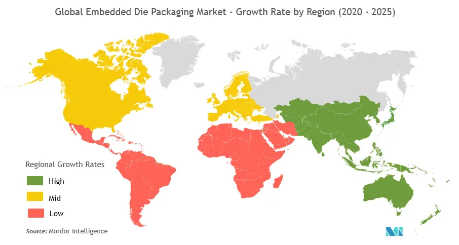
| Fastest Growing Market | Asia Pacific |
| Largest Market | North America |
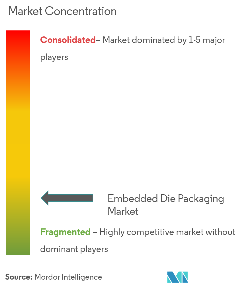
| Market Concentration | Low |
Major Players
*Disclaimer: Major Players sorted in no particular order |
Embedded Die Packaging Market Analysis
The embedded die packaging market was valued at USD 52.3 billion in 2020 and is expected to reach USD 175.27 billion by 2026 has been expected to grow at a CAGR of 22.4% during the forecast period (2021 - 2026). 3D packaging with embedded die solutions has become more attractive as an integration tool for next-generation devices which will become a key trend in future.
- Growing miniaturization of devices is driving the market as products are becoming increasingly smaller and embed more functionality. Micromachining and nanotechnology play an increasingly important role in the miniaturization of components ranging from biomedical applications to chemical microreactors and sensors. For instance, Bluetooth wifi modules requires minimal circuit board area on today's high-density mobile devices.
- Improved electrical & thermal performance is driving the market. For power management and mobile-wireless application the embedded technology has been evaluated to replace assembles fabrication by not only thinner thickness but due to superior thermal performance. The thermal performance of embedded die is better than PQFN with copper clip about 17%. Also a new and expandable advanced package for power devices is developed using embedded dies and redistribution layer (RDL) technology for electric car to improve the electric and thermal performance.
- Further, owing to its excellent electrical performance at high frequencies, the technology is also being perceived as a promising technology for emerging telecommunication applications. Various advantages that aid the deployment of the technology in telecommunication applications include increased functionality and efficiency of the electronic circuits, power and signal inductance, improved reliability, and higher signal density.
- Difficulty to test, inspect and rework, the embedded die technology challenges the market to grow. As features (lines and spaces) shrink to 2µm and below, it becomes more difficult to see defects. In addition, finding debris in via holes becomes a concern in some applications.
- Since the outbreak of COVID-19, the electronics industry has been hit severely, with a significant influence on its supply chain and production facilities. The production came to a stand still in China and Taiwan during February and March, which influenced various OEMs across the world.
Embedded Die Packaging Market Trends
This section covers the major market trends shaping the Embedded Die Packaging Market according to our research experts:
Die in Flexible Board Expected to Hold Significant Market Share
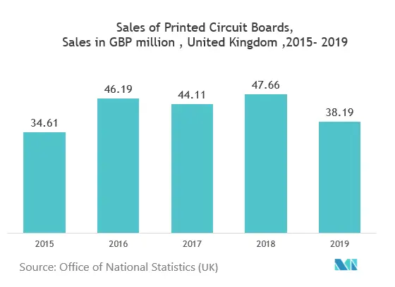
- With the increased advancement in technology, the product sale value of the printed circuit board is increasing and with the increased adoption of the flexible board in various wearable and IoT devices, the sales are expected to grow higher in future.
- Stretchable Electronics (SC) is so far commercial and comes in many shapes and forms. The technology uses standard printed circuit board, mainly flexible board, where liquid injection molding techniques involve elastomer embedded stretchable electronic circuit, which achieves a robust and reliable product. For instance, in military usage, uniforms and armors can have embedded, flexible, lightweight impact sensors that could store and provide better information of the injury sustained during combat.
- Flexible hybrid electronics (FHE), which is considered as a novel approach to electronic circuit manufacturing, aims to combine the best of conventional and printed electronics. Additional components and as many as conductive interconnects are possible to be printed onto a flexible substrate, whereas the IC is produced using photolithography and then mounted, as a bare die.
- The embedding activity of flexible circuits are in high trend for their implementation in various miniature electronic devices. For instance, in September 2019, IDEMIA and Zwipe collaborated for a biometric payment card solution, where the solution is planned to be distinguished by its relatively small number of components, with things, like the Secure Element and the microcontroller, all embedded in a single chip mounted on a flexible printed circuit board.
- Further, autonomous systems for sports applications and healthcare mainly benefit from a small form factor, as minute structures result in maximal flexibility and comfort. The embedding of a commercially available IC in a flexible circuit board (FCB) can reduce the overall size of a system. The usage of liquid crystal polymer (LCP) as base material for sensors are highly used in medical products. Miniaturized smart sensor modules for medical applications can be fabricated from LCP substrates using conventional flex circuit thin film and standard assembly processes and equipment.
North America Expected to Hold Significant Market Share
- Countries in the region, such as United States assist the world in manufacturing, designing, and researching related to the semiconductor industry and United States is also the frontrunner in semiconductor packaging innovation having 80 wafer fabrication plants spread across 19 states where new technologies is being implemented such as miniaturization through embedded die etc. Apart from this, investments in this country by global players are setting to fuel the market.
- For instance, Intel is enabling Next-Generation Platforms using Intel’s 3D System-in-package technology through Embedded Multi-die Interconnect Bridge (EMIB) , an elegant and cost-effective approach to in-package high density interconnect of heterogeneous chips. The industry refers to this application as 2.5D package integration. Instead of using a large silicon interposer typically found in other 2.5D approaches, Embedded Multi-die Interconnect Bridge (EMIB) uses a very small bridge die, with multiple routing layers. This bridge die is embedded as part of our substrate fabrication process.
- Apart from this, the United States is home to some of the major automotive players in the world, which are investing in the electric car segment. The embedded systems increases the driving comfort with driver assistance functions like adaptive cruise control. Also to achieve significant energy savings, a distributed embedded control approach becomes necessary to control the power management of the entire vehicle. This is set to increase the demand for embedded die technology.
Embedded Die Packaging Industry Overview
The embedded die packaging market is fragmented due to the growing number of end-users in automotive, industrial, and consumer electronics. The existing players in the market are striving to maintain a competitive edge by catering to newer technologies, such as 5G telecommunication, high-performance data centers, compact electronic devices, etc. Key players are Microsemi Corporation, Fujikura Ltd, etc. Recent developments in the market are -
- October 2020 - The U.S. Department of Defence awarded Intel Federal LLC the second phase of its Heterogeneous Integration Prototype (SHIP) program. The SHIP program enables the US government to access Intel's state-of-the-art semiconductor packaging capabilities in Arizona and Oregon and take advantage of capabilities created by Intel's tens of billions of dollars of annual R&D and manufacturing investment. The project is executed by the Naval Surface Warfare Centre, Crane Division, and administered by the National Security Technology Accelerator.
- Sep 2019 - Achronix Semiconductor Corporation, a leading supplier in FPGA-based hardware accelerator devices and high-performance eFPGA IP, joined the TSMC IP Alliance Program, a key component of TSMC Open Innovation Platform (OIP). Achronix demonstrated how its Speedcore IP is uniquely sized and optimized for each customer's application in its booth at TSMC Open Innovation Platform Ecosystem Forum.
Embedded Die Packaging Market Leaders
-
Microsemi Corporation
-
Fujikura Ltd.
-
Infineon Technologies AG
-
ASE Group
-
AT&S Company
*Disclaimer: Major Players sorted in no particular order
Embedded Die Packaging Market Report - Table of Contents
-
1. INTRODUCTION
-
1.1 Study Assumptions and Market Definition
-
1.2 Scope of the Study
-
-
2. RESEARCH METHODOLOGY
-
3. EXECUTIVE SUMMARY
-
4. MARKET DYNAMICS
-
4.1 Market Overview
-
4.2 Market Drivers
-
4.2.1 Growing Miniaturization of Devices
-
4.2.2 Improved Electrical and Thermal Performance
-
-
4.3 Market Restraints
-
4.3.1 Difficulty to Inspect, Test and Rework
-
-
4.4 Industry Value Chain Analysis
-
4.5 Industry Attractiveness - Porter's Five Forces Analysis
-
4.5.1 Bargaining Power of Suppliers
-
4.5.2 Bargaining Power of Buyers/Consumers
-
4.5.3 Threat of New Entrants
-
4.5.4 Threat of Substitute Products
-
4.5.5 Intensity of Competitive Rivalry
-
-
4.6 Impact of COVID-19 on the Market
-
-
5. TECHNOLOGY SNAPSHOT
-
5.1 PCB Miniaturization
-
5.2 Advanced Embedded Active System Integration
-
-
6. MARKET SEGMENTATION
-
6.1 Platform
-
6.1.1 Die in Rigid Board
-
6.1.2 Die in Flexible Board
-
6.1.3 IC Package Substrate
-
-
6.2 End User
-
6.2.1 Consumer Electronics
-
6.2.2 IT and Telecommunications
-
6.2.3 Automotive
-
6.2.4 Healthcare
-
6.2.5 Other End Users
-
-
6.3 Geography
-
6.3.1 Americas
-
6.3.2 Europe and MEA
-
6.3.3 Asia-Pacific
-
-
-
7. COMPETITIVE LANDSCAPE
-
7.1 Company Profiles
-
7.1.1 Microsemi Corporation
-
7.1.2 Fujikura Ltd
-
7.1.3 Infineon Technologies AG
-
7.1.4 ASE Group
-
7.1.5 AT&S Company
-
7.1.6 Schweizer Electronic AG
-
7.1.7 Intel Corporation
-
7.1.8 Taiwan Semiconductor Manufacturing Company
-
7.1.9 Shinko Electric Industries Co. Ltd
-
7.1.10 Amkor Technology
-
7.1.11 TDK Corporation
-
- *List Not Exhaustive
-
-
8. INVESTMENT ANALYSIS
-
9. MARKET OPPORTUNITIES AND FUTURE TRENDS
Embedded Die Packaging Industry Segmentation
Embedded die is described as a passive component or an IC (integrated circuit) that is placed or formed on an inner layer of an organic circuit board, module, or chip package. With increase in number of portable electronic devices, rise in application in healthcare and automotive devices, and advantages over other advanced packaging technologies is driving the market growth.
| Platform | |
| Die in Rigid Board | |
| Die in Flexible Board | |
| IC Package Substrate |
| End User | |
| Consumer Electronics | |
| IT and Telecommunications | |
| Automotive | |
| Healthcare | |
| Other End Users |
| Geography | |
| Americas | |
| Europe and MEA | |
| Asia-Pacific |
Embedded Die Packaging Market Research FAQs
What is the current Embedded Die Packaging Market size?
The Embedded Die Packaging Market is projected to register a CAGR of 22.40% during the forecast period (2024-2029)
Who are the key players in Embedded Die Packaging Market?
Microsemi Corporation, Fujikura Ltd., Infineon Technologies AG, ASE Group and AT&S Company are the major companies operating in the Embedded Die Packaging Market.
Which is the fastest growing region in Embedded Die Packaging Market?
Asia Pacific is estimated to grow at the highest CAGR over the forecast period (2024-2029).
Which region has the biggest share in Embedded Die Packaging Market?
In 2024, the North America accounts for the largest market share in Embedded Die Packaging Market.
What years does this Embedded Die Packaging Market cover?
The report covers the Embedded Die Packaging Market historical market size for years: 2019, 2020, 2021, 2022 and 2023. The report also forecasts the Embedded Die Packaging Market size for years: 2024, 2025, 2026, 2027, 2028 and 2029.
Embedded Die Packaging Industry Report
Statistics for the 2024 Embedded Die Packaging market share, size and revenue growth rate, created by Mordor Intelligence™ Industry Reports. Embedded Die Packaging analysis includes a market forecast outlook to 2029 and historical overview. Get a sample of this industry analysis as a free report PDF download.


