Market Size of Global Dielectric Etchers Industry

| Study Period | 2019 - 2029 |
| Base Year For Estimation | 2023 |
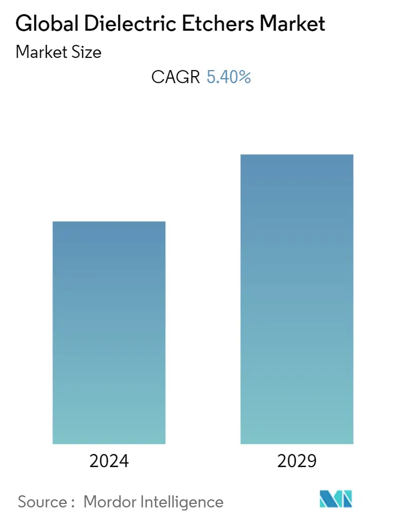
| CAGR | 5.40 % |
| Fastest Growing Market | Asia Pacific |
| Largest Market | Asia Pacific |
| Market Concentration | Low |
Major Players
*Disclaimer: Major Players sorted in no particular order |
Dielectric Etchers Market Analysis
The Global Dielectric Etchers Market is expected to register a CAGR of 5.4% during the forecast period 2022 to 2027. The increasing demand for miniaturizing the ICs to be used in compact & mobile devices is expected to drive the market. The current electronic devices use semiconductors of circuit line width, which ranges from 5 - 20 nm; however, the emergence of atomic-level etching process & demand for miniaturized IC, which consumes less power, will push the circuit line width range to 0 - 10 nm.
- An increase in demand for neuromorphic chips will drive the market for etchers. The rising demand for artificial intelligence, data processing & analytics is a major factor influencing the innovation & adoption of neuromorphic chips across the globe. Etch techniques aid in creating chip features by eliminating coatings and materials put on the wafer selectively. These procedures entail producing increasingly small and intricate features with difficult-to-remove material combinations.
- The latest trend in the global dielectric etchers market is the emergence of 3D ICs. With the increasing demand for faster computing devices that consume less amount of energy will significantly drive the demand for 3D chip stacking. The growing need for miniaturizing electronic devices in fields such as Aerospace, Automotive & Medical sectors will drive the demand for dielectric etchers, which are capable of altering structures to a precision of 0 - 10 nm & even at an atomic level.
- Etch methods also produce tall, high-aspect-ratio features, like through-silicon vias (TSVs), which allow chip packaging and micro-electromechanical system integration (MEMS). For instance, Lam Research plasma etch systems provide high-performance and high-productivity capabilities required to build precise structures, ranging from tall and narrow, short and wide, to a few angstroms in size.
- In May 2021, Applied Materials, Inc. announced three new materials engineering solutions that enable its memory customers three new options to scale DRAM and optimize chip performance, power, area, cost, and time to market (PPACt). DRAM manufacturers use black diamond, a low-k dielectric material developed by Applied Materials, to solve logic interconnect scalability problems.
- The outbreak of COVID-19 significantly disrupted the supply chain and production during the initial phase of 2020. The impact was more severe for semiconductor manufacturers, the major end users for semiconductor etch equipment. Due to labor shortages, many players in the semiconductor supply chain had to reduce or even suspend their operations. The industry was riddled with a high deficit and increasing demand, which led to a significant supply chain gap. The initial spread of the virus led to the shutting down or reduction of foundry capacity utilization, fearing the decreasing demand for chips across major sectors, like the automotive. Diminished output led to a global shortage of semiconductors as demand increased, despite the initial estimates by semiconductor foundries.
Dielectric Etchers Industry Segmentation
The Global Dielectric Etchers Market is segmented by Type (Wet Etching, Dry Etching, Atomic Level Etching) and by Geography. For dielectric etching, were to etch rate is not a significant driver, traditional diode-type chambers are used, else the high-density plasma systems are used. In some cases, manufacturers have added magnetic enhancement to these basic systems to reduce sidewall losses and confine the plasma. With an increasing demand for high-performance chipsets in mobile devices and faster semiconductor manufacturing techniques, dielectric etching is increasingly becoming popular with foundries. With the emergence of Atomic-Level Etching, foundries are better equipped to meet the demands of the customers, even to miniaturize the circuit width lining.
| By Type | |
| Wet Etching | |
| Dry Etching | |
| Atomic Level Etching (ALE) |
| By Geography | |
| North America | |
| Europe | |
| Asia Pacific | |
| Rest of the World |
Global Dielectric Etchers Market Size Summary
The global dielectric etchers market is poised for significant growth, driven by the increasing demand for miniaturized integrated circuits (ICs) used in compact and mobile devices. As electronic devices evolve, the need for semiconductors with smaller circuit line widths is becoming paramount, pushing the industry towards atomic-level etching processes. This trend is further fueled by the rising demand for neuromorphic chips, which are essential for advanced artificial intelligence, data processing, and analytics applications. The market is also witnessing a surge in the adoption of 3D ICs, driven by the need for faster, energy-efficient computing devices. Sectors such as aerospace, automotive, and medical are contributing to this demand, necessitating etchers capable of precise alterations at the atomic level.
The competitive landscape of the global dielectric etchers market is characterized by the presence of both small and large players, with major companies like Applied Materials Inc., Hitachi High-Technologies Corporation, and Lam Research Corporation holding significant market shares. These companies are actively expanding their consumer base through partnerships and the introduction of innovative products. The market's growth is also supported by advancements in atomic layer etching (ALE) technology, which is crucial for achieving the accuracy required for sub-10nm device features. The collaboration between industry leaders, such as Tokyo Electron and IBM, highlights the ongoing efforts to streamline semiconductor production processes, addressing challenges like the global chip shortage. As the demand for advanced semiconductors continues to rise, the dielectric etchers market is expected to experience robust expansion.
Global Dielectric Etchers Market Size - Table of Contents
-
1. MARKET INSIGHTS
-
1.1 Market Overview
-
1.2 Industry Attractiveness - Porter's Five Forces Analysis
-
1.2.1 Bargaining Power of Suppliers
-
1.2.2 Bargaining Power of Consumers
-
1.2.3 Threat of New Entrants
-
1.2.4 Threat of Substitutes
-
1.2.5 Intensity of Competitive Rivalry
-
-
1.3 Impact of COVID-19 on the Market
-
-
2. MARKET SEGMENTATION
-
2.1 By Type
-
2.1.1 Wet Etching
-
2.1.2 Dry Etching
-
2.1.3 Atomic Level Etching (ALE)
-
-
2.2 By Geography
-
2.2.1 North America
-
2.2.2 Europe
-
2.2.3 Asia Pacific
-
2.2.4 Rest of the World
-
-
Global Dielectric Etchers Market Size FAQs
What is the current Global Dielectric Etchers Market size?
The Global Dielectric Etchers Market is projected to register a CAGR of 5.40% during the forecast period (2024-2029)
Who are the key players in Global Dielectric Etchers Market?
Applied Materials, Inc., Hitachi High-Technologies Corporation, Lam Research Corporation, Tokyo Electron and Mattson Technology, Inc. are the major companies operating in the Global Dielectric Etchers Market.

