Market Overview
| Study Period | 2020 - 2031 |
|---|---|
| Market Size (2026) | USD 2.13 Billion |
| Market Size (2031) | USD 3.49 Billion |
| Growth Rate (2026 - 2031) | 10.36 % |
| Fastest Growing Market | Asia-Pacific |
| Largest Market | North America |
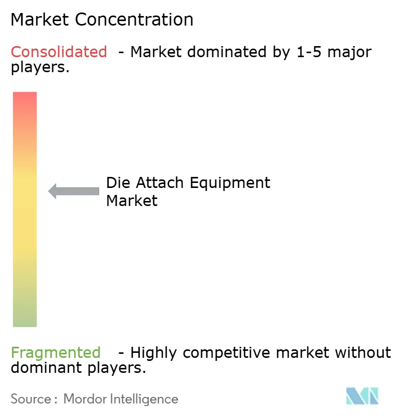
| Market Concentration | Medium |
Major Players *Disclaimer: Major Players sorted in no particular order Image © Mordor Intelligence. Reuse requires attribution under CC BY 4.0. | |
Die Attach Equipment Market Analysis by Mordor Intelligence
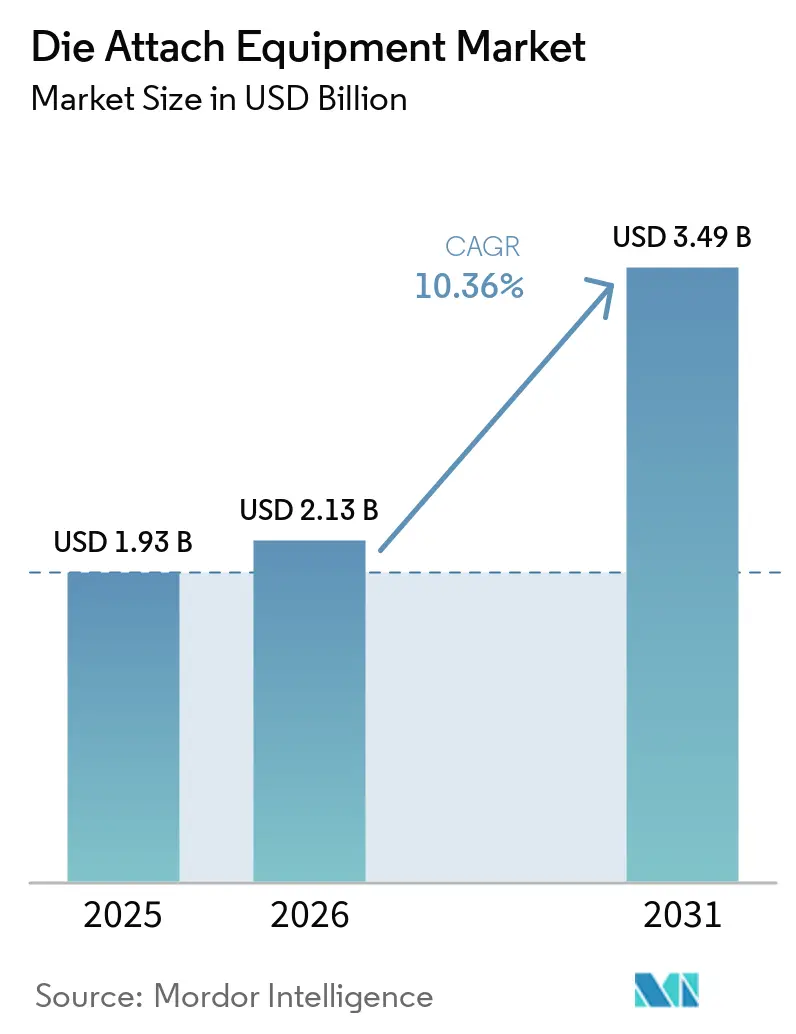
Die attach equipment market size in 2026 is estimated at USD 2.13 billion, growing from 2025 value of USD 1.93 billion with 2031 projections showing USD 3.49 billion, growing at 10.36% CAGR over 2026-2031. Government incentives that localize semiconductor supply chains, rapid electrification of vehicles, and the surge of chiplet-based AI accelerators collectively keep capital spending on new bonding tools on an expansionary path. In parallel, wide-bandgap device adoption is pushing process temperatures and pressure profiles higher, while mini-LED backlights and emerging micro-display fabs demand sub-5 µm placement repeatability. Equipment suppliers are reacting with hybrid architectures that merge flip-chip, eutectic, and pressure-sintering heads on a single chassis so that contract manufacturers can tackle heterogeneous integration without line changeovers. Larger average selling prices for these configurable platforms are buffering vendors against smartphone-centric slowdowns, and process control software that captures bond-by-bond traceability is emerging as a differentiator in customer qualification audits.
Key Report Takeaways
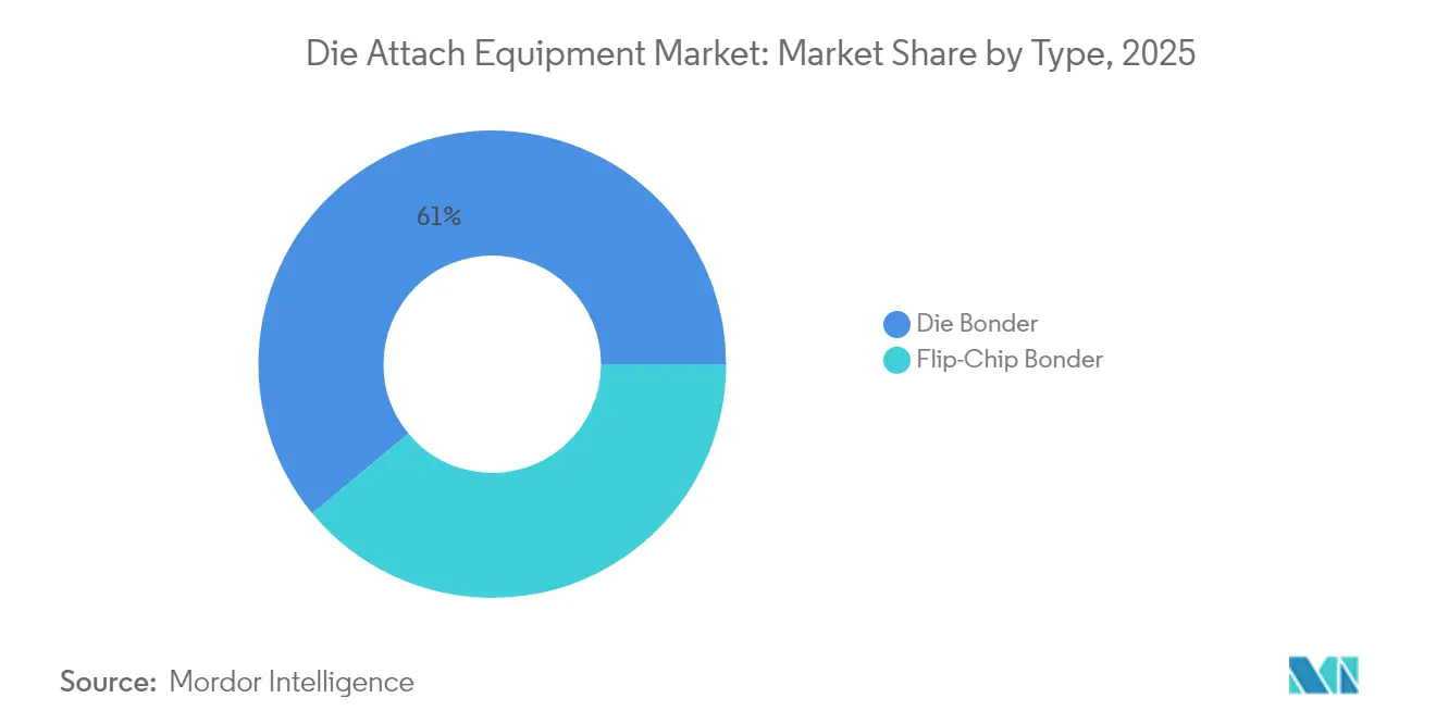
- By bonder type, die bonders led with 61.02% of die attach equipment market share in 2025, while flip-chip bonders are projected to log an 11.35% CAGR through 2031.
- By bonding technique, epoxy accounted for 37.64% of the die attach equipment market size in 2025; hybrid bonding is forecast to expand at a 11.58% CAGR to 2031.
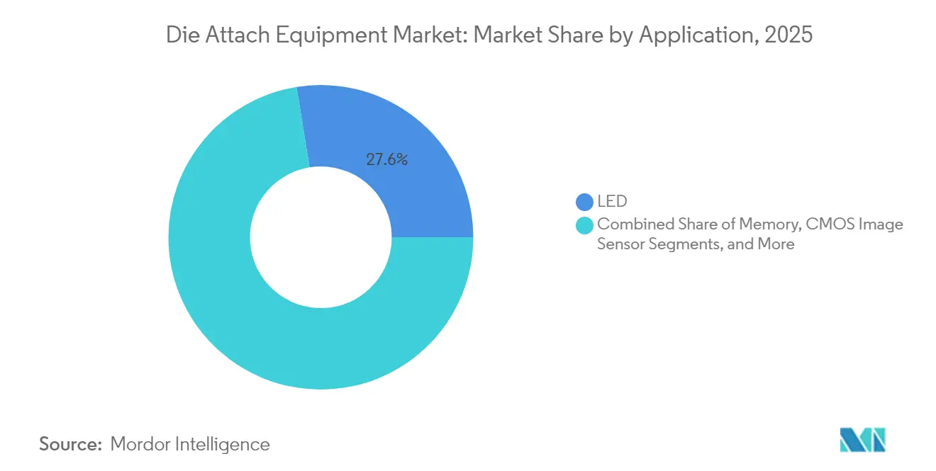
- By application, LED manufacturing contributed 27.55% of the die attach equipment market size in 2025, and optoelectronics/photonics is advancing at a 12.96% CAGR through 2031.
- By end-user industry, consumer electronics held 32.74% of the die attach equipment market share in 2025, whereas automotive and transportation record the highest projected CAGR at 14.02% between 2026 and 2031.
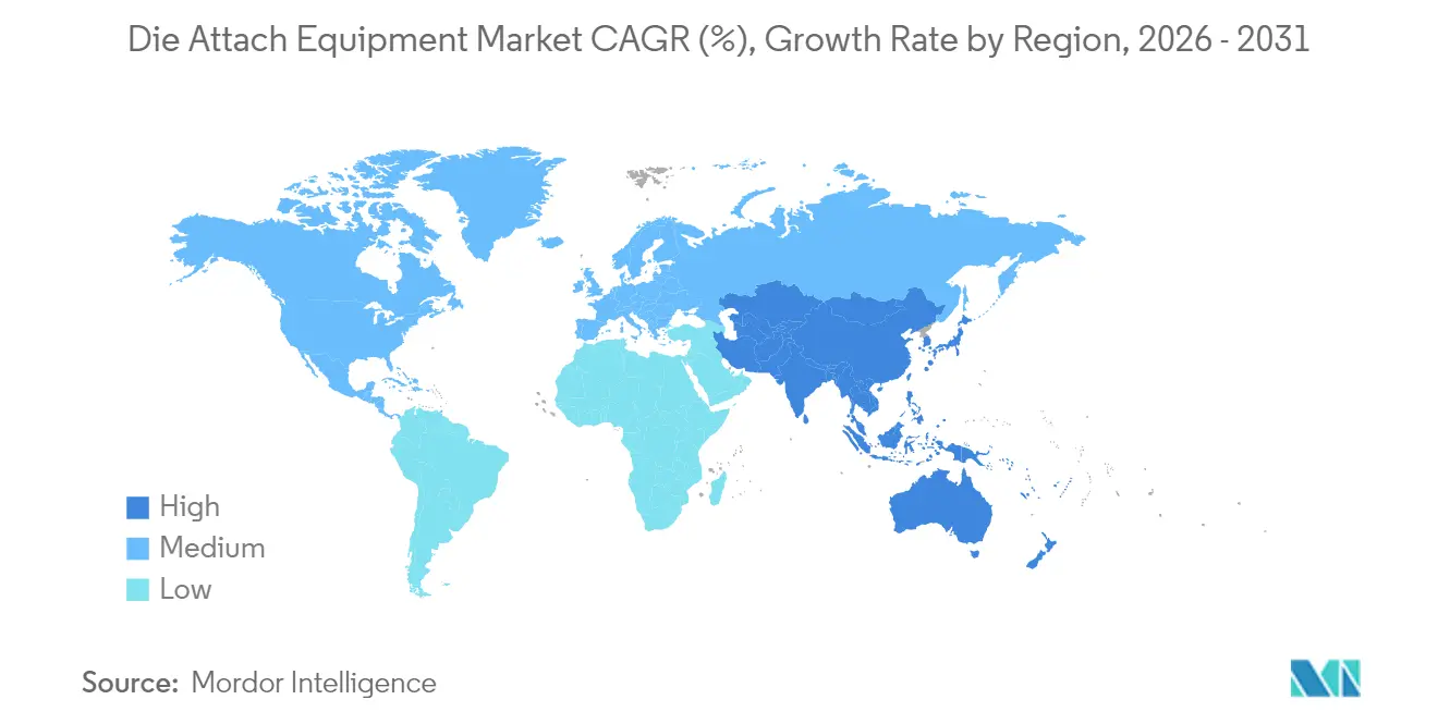
- By geography, North America captured 55.05% of the die attach equipment market size in 2025; Asia-Pacific is rising at a 13.31% CAGR to 2031.
Note: Market size and forecast figures in this report are generated using Mordor Intelligence’s proprietary estimation framework, updated with the latest available data and insights as of 2026.
Market Trends and Insights
Drivers Impact Analysis of Die Attach Equipment Market*
| Driver | (~) % Impact on CAGR Forecast | Geographic Relevance | Impact Timeline |
|---|---|---|---|
| Expansion of AuSn eutectic die-attach in advanced RF modules | +1.80% | Global, with early gains in North America, Europe | Medium term (2-4 years) |
| Proliferation of SiC/GaN discrete power devices in EV inverters | +2.30% | APAC core, spill-over to North America & EU | Short term (≤ 2 years) |
| LED mini-/micro-display capacity build-out in Asia | +1.50% | APAC, particularly China, Taiwan, South Korea | Short term (≤ 2 years) |
| Heterogeneous integration demand for Chiplet-based AI accelerators | +2.10% | Global, with concentration in Taiwan, North America | Medium term (2-4 years) |
| Government CHIPS-style fab equipment incentives outside the US | +1.40% | North America, EU, with expansion to India, Japan | Long term (≥ 4 years) |
| Shift toward high-mix, low-volume photonics packaging lines | +0.90% | North America & EU, niche expansion to APAC | Long term (≥ 4 years) |
| Source: Mordor Intelligence | |||
Expansion of AuSn eutectic die-attach in advanced RF modules
Gold–tin eutectic bonding has regained popularity because 5G millimeter-wave and satellite payloads dissipate higher heat loads than legacy epoxy joints can handle. The 80/20 alloy melts at 280 °C yet keeps thermal conductivity near 57 W/mK, enabling hermetic packages that survive thermal cycling in aerospace and defense deployments.[1]Palomar Technologies, “Technical Papers & e-Books,” palomartechnologies.com Pulsed-heat tools confine energy to the joint area and prevent substrate warpage, which historically limited AuSn adoption on larger laminated boards. Although volume remains modest, margins are attractive and justify premium equipment pricing as OEMs tighten longevity specifications for mission-critical radios.
Proliferation of SiC/GaN discrete power devices in EV inverters
Silicon carbide and gallium nitride switches sustain junction temperatures above 200 °C, so automotive Tier-1s are migrating from epoxy to pressure-sintered silver layers that lower thermal resistance and eliminate voids.[2]Bozhon Semiconductor, “FastStar Series,” bozemi.com New die attach platforms incorporate closed-loop pressure monitoring and controlled-atmosphere chambers that complete sintering in less than 3 minutes, outperforming earlier six-minute cycles. Because vehicle programs lock production tooling two years before SOP, equipment suppliers enjoy predictable bookings, yet purchasing waves remain synchronized with model-year launches, leading to revenue lumpiness.
LED mini-/micro-display capacity build-out in Asia
Display makers racing toward direct-view mini-LED backlights are specifying placement repeatability tighter than 3 µm, up from 7 µm tolerances in 2023. Throughput targets now exceed 70 kUPH for mini-LED arrays, requiring parallel pick heads and dual high-resolution vision stacks to identify dice as small as 50 × 125 µm on the fly.[3]ITEC, “Die Attach Solutions,” itecequipment.com Suppliers offering embedded optical binning are winning contracts because they eliminate post-bond inspection stages, shaving two seconds off cycle time per module and freeing floor space in high-cost cleanrooms.
Heterogeneous integration demand for chiplet-based AI accelerators
High-performance GPUs and custom inference engines are shifting to chiplet layouts to sidestep reticle-size limits. Die attach equipment must therefore place compute, HBM, and I/O tiles within 1 µm tolerance so that subsequent hybrid bonding forms low-resistance Cu–Cu interconnects. Vendors integrate machine-learning vision algorithms that classify fiducials under non-uniform lighting, while linear-motor and air-bearing stages deliver 20 nm step resolution.[4]Mycronic, “Microelectronics Die Bonding Systems,” mycronic.com Systems shipping into this niche command ASPs above USD 3 million and generate service annuities because software upgrades extend tool life across successive process nodes.
Restraints Impact Analysis of Die Attach Equipment Market*
| Restraint | (~) % Impact on CAGR Forecast | Geographic Relevance | Impact Timeline |
|---|---|---|---|
| Dimensional changes and mechanical unbalance during thermo-compression | -1.20% | Global, particularly affecting advanced packaging | Short term (≤ 2 years) |
| Cyclical slow-down in smartphone CMOS image-sensor cap-ex | -0.80% | APAC core, with secondary impact on North America | Medium term (2-4 years) |
| Talent shortage for sub-5 µm placement accuracy assembly engineers | -0.60% | Global, most acute in North America & Europe | Long term (≥ 4 years) |
| Supply-chain exposure to indium and gold price volatility | -0.40% | Global, with higher impact on cost-sensitive applications | Short term (≤ 2 years) |
| Source: Mordor Intelligence | |||
Dimensional changes and mechanical unbalance during thermo-compression
Thermo-compression bonding exposes substrates to 300 °C loads that trigger differential expansion between silicon, organics, and metal pillars. Warpage exceeding 400 µm causes non-contact points and degrades yield, especially on 90 × 110 mm panels. Although inline metrology now feeds Z-axis corrections to bond heads in real time, physics still caps panel size and slows production ramp-ups. Users consequently run smaller lots while process windows stabilize, lowering overall tool utilization.
Cyclical slow-down in smartphone CMOS image-sensor cap-ex
Global smartphone shipments fell 3.2% in 2024, prompting major sensor fabs to cut capital budgets 15-20% and defer tool deliveries.[5]Semiconductor Industry Association, “CHIPS Act Implementation,” semiconductors.org Because CMOS image-sensor lines dominate die bonding volume in East Asia, equipment orders retraced for two consecutive quarters. Offsetting growth emerges from automotive ADAS cameras, but those projects use smaller wafer starts and cannot fully compensate for handset softness, introducing volatility into quarterly revenue for several toolmakers.
*Our forecasts treat driver/restraint impacts as directional, not additive. The impact forecasts reflect baseline growth, mix effects, and variable interactions.
Die Attach Equipment Market Segment Analysis
By Bonder Type:
Flip-chip momentum challenges die-bonder incumbencyDie bonders commanded 61.02% of 2025 revenue and remained the workhorse for wire-bonded packaging, memory stacks, and cost-optimized consumer electronics lines, giving them the single-largest slice of the die attach equipment market size. OEMs appreciate the mature process libraries, low consumables cost, and broad operator familiarity these tools deliver, supporting continued demand across the die bonder equipment market. Yet flip-chip platforms are climbing at an 11.35% CAGR as 2.5D interposers and chip-on-wafer-on-substrate flows move from pilot to volume. Increasingly, contract manufacturers want one chassis that can swap feed heads so that both eutectic die and bump-first flip-chips ride the same conveyor. Tool vendors reply with modular decks whose changeover completes in under 8 minutes.
Hybrid product families blur distinctions between bonder types. Stage kinematics now borrow from lithography steppers, with air bearings and linear motors pushing placement three-sigma below 1 µm. Software orchestrates multi-tool cells, routing jobs to the die bonder or flip-chip head according to tape width and solder-mask windows. This flexibility lets customers amortize capital across broader order books, and the strategy secures stickier service contracts for OEMs pivoting toward recurring revenue. The result is tighter competition as emerging vendors court niches such as compound-semiconductor lasers while stalwarts safeguard share in the bulk commodity compute segment.


By Bonding Technique:
Hybrid bonding narrows the gapEpoxy processes held 37.64% of 2025 revenue thanks to material affordability and relaxed thermal budgets that fit legacy ovens, anchoring the largest portion of the die attach equipment market share. Dispense-then-place remains indispensable in sensor and RF-front-end modules where gap-filling counters die thickness variation. Nonetheless, equipment orders for hybrid bonding post 11.58% CAGR as copper-to-copper micro-bumpless contacts sprint ahead of interposer limits.
Hybrid-capable bonders integrate wafer-level planarization checkpoints that verify Cu pad co-planarity within 30 nm, then transition to die-level pick-and-place without breaching the Class 1 clean constraint. Applied Materials’ USD 2.8 billion equity move in Besi underscores the capital intensity required to master this overlay. For users, the step change promises signal latency drops of 35 ps per hop, translating to 5% overall inference speedup in AI accelerators. Yet first-pass yields still lag epoxy by 200 basis points, so adoption centers on premium devices where the ASP cushion absorbs yield drag.
By Application:
Photonics steps into the spotlightLED assembly secured 27.55% of 2025 demand, riding the replacement of fluorescent backlights and the rise of energy-efficient architectural lighting. High-speed carousel pick heads that bond four chips per second keep cost per lumen competitive against OLED. However, optoelectronics and photonics equipment logs a faster 12.96% CAGR, grabbing cap-ex budgets as cloud operators extend 800 G and 1.6 T fiber links and coherent pluggables migrate to shorter reaches.
Photonics packaging obliges sub-micron Z-axis coplanarity so optical axes line up within 0.2 µm, a tougher metric than electrical pad attachment. New bonders therefore embed fringe-field interferometers for in-situ alignment using live optical feedback instead of post-bond rejection. Simultaneous dispense of low-shrink epoxies curbs stress on glass-through-silicon vias, a feature that telephone modules rarely need. Vendors that pre-engineer photonic-specific nests and reflectometry options lock in tool share early because retrofitting general-purpose bonders proves cost-prohibitive after cleanroom hook-up.
By End-User Industry:
Electrified mobility accelerates spendConsumer electronics retained 32.74% of 2025 shipments, leveraging fully depreciated high-volume bonders that withstand narrow factory margins in handset and tablet production. Nevertheless, EV makers are on pace for a 14.02% CAGR in equipment purchases as traction inverters, onboard chargers, and autonomous driving sensors proliferate. Silver-sinter bonders that tolerate 200 °C junctions and 3,000 thermal cycles underpin this growth.
The lengthy automotive PPAP qualification, which spans two years, gives tool vendors visibility but imposes documentation rigor that disqualifies some smaller entrants. Industrial power segments supply baseline demand for motor drives and solar inverters, while telecom and datacom keep incremental orders alive for 5G radios and data-center switches. Aerospace programs, though niche, pay premiums for hermetic AuSn process modules that survive proton radiation in LEO constellations. Collectively, these niches help cushion suppliers over the smartphone troughs that periodically hit Asian OSAT lines.
Geography Analysis
North America Die Attach Equipment Market
North America controlled 55.05% of 2025 revenue, leveraging the CHIPS Act’s USD 52 billion grants that redirect tool budgets toward domestic fabs. Major tool clusters sit in California and Arizona where process engineers co-locate with design teams from Intel, Nvidia, and AMD. Coupled with strong defense contracts that favor U.S. soil assembly, these dynamics keep premium-price hybrid bonders booked through 2026. Clean-energy subsidies also encourage regional SiC module lines, adding a dependable equipment pull outside traditional microprocessor channels.
Europe Die Attach Equipment Market
Europe follows at a steady pace, buoyed by Infineon and STMicroelectronics expanding wide-bandgap pilot fabs in Germany and Italy. Automotive OEMs anchor demand curves, especially as EU emissions mandates tighten and inverter efficiencies become buying criteria for fleet managers. Although volume manufacturing sometimes migrates to Asian OSAT partners, initial capacity ramps occur domestically so that quality teams can iterate faster. This localized prototyping preserves a portion of bonding tool orders within the bloc and ensures compliance with future carbon-audit frameworks envisioned under the Green Deal.
APAC Die Attach Equipment Market
Asia-Pacific posts the quickest 13.31% CAGR to 2031 as Taiwan’s TSMC pours more than USD 10 billion yearly into CoWoS and SoIC lines serving AI chips. South Korea’s memory titans add flip-chip capacity to package next-gen HBM, while Chinese policy banks extend low-interest loans that finance domestically sourced bonders when export licenses stall. Despite intellectual-property headwinds, several local OEMs replicate legacy die bonder functionality and bundle aggressive service terms, expanding price competition. The region’s density of contract manufacturers lowers response time, allowing quick diffusion of process tweaks across ecosystem partners.

Regulatory Landscape
Export controls around semiconductor manufacturing equipment and related software are a key regulatory variable shaping die attach tool shipments and service support globally. In the United States, the Bureau of Industry and Security (BIS) administers the Export Administration Regulations (EAR), including controls implemented via ECCNs and extraterritorial levers such as the Foreign Direct Product Rule (FDPR). In December 2024, BIS issued an interim final rule amending the EAR to control certain semiconductor manufacturing equipment and related software keys, with staged effective dates in December 2024.
Compliance interpretation has also tightened in 2026. In May 2026, BIS published guidance clarifying license requirements for exports of advanced computing items to entities tied to Country Group D:5 or Macau through a headquartered-in or ultimate-parent test, affecting how suppliers screen counterparties and structure channel sales. In Europe, the European Commission updated the EU dual-use export control list through a Delegated Regulation adopted in September 2025, adding another layer of cross-jurisdiction compliance for deployed die attach platforms, spare parts, software, and service workflows.
Value Chain Analysis
The die attach equipment value chain starts with precision subsystems and materials that enable placement accuracy and repeatable bonding profiles, including motion stages (linear motors, air bearings), high-resolution vision and illumination stacks, force and temperature control, controlled-atmosphere enclosures, and software for recipe management and bond-by-bond traceability. Upstream inputs also include bonding consumables and process enablers such as epoxies, AuSn preforms, and silver sinter pastes, which shape tool configuration for dispense, eutectic, thermo-compression, or sinter heads. Tool OEMs integrate these elements into platforms sold directly to IDMs and foundries, or through OSAT-focused sales and application engineering teams, with installation, qualification, and field service forming a substantial part of delivered value, particularly for sub-5 um and hybrid bonding-capable systems.
Downstream, demand concentrates in advanced packaging and high-reliability assembly lines, where equipment interoperability and qualification cycles drive total cost of ownership. SEMI reported assembly and packaging equipment billings rising 21% year-over-year in 2025, reflecting stronger back-end spend and reinforcing the role of OSATs, substrate suppliers, and module integrators in purchase decisions. Bottlenecks increasingly come from integration rather than component availability, with 68% of Taiwan fabs citing equipment compatibility constraints, including mechanical interface mismatches (including FOUP-related issues). This shifts spend toward custom engineering, adapter kits, and software integration work. Lead-time risk also remains a factor, with survey-based supply chain metrics showing a higher share of respondents reporting increased equipment lead times in 2025 versus 2024, encouraging customers to lock configurations earlier and favor vendors with local applications support and multi-sourced critical subsystems.
Competitive Landscape
Industry incumbents, ASM Pacific Technology, MicroAssembly Technologies, and Besi, still sit atop revenue tables by virtue of broad portfolios that span wire bond, flip-chip, and hybrid bonding stations. Each vendor offers unified software suites that standardize recipe management, letting contract manufacturers shuffle labor between SMT and packaging lines without extra training. Yet the die attach equipment market is not static; mid-tier innovators like Mycronic and Palomar Technologies are winning design-in slots where sub-micron accuracy trumps unit throughput. Their platforms use air bearings and closed-loop thermal expansion control borrowed from aerospace machining, moving them into higher-margin verticals.
Strategic tie-ups are reshaping share. Applied Materials 9% stake in Besi injects front-end process know-how into back-end assembly, producing an integrated flow that pulls wafers straight from CMP into die-level hybrid bonding. Chinese challengers such as Bozhon Semiconductor lure cost-sensitive buyers with 3,000-UPH mid-accuracy units that undercut foreign prices by 20%, eroding volume at the low end and pressuring incumbents to differentiate.
Niche players focus on photonics and compound semiconductors. SUSS MicroTec tunes bond heads for 2 × 3 mm InP laser chips that feed co-packaged optics, while Palomar’s 3880-II adopts pulsed-heat eutectic for defense-grade RF components. Because these applications carry high ASPs, even single-digit shipment volumes materially affect revenue mix. Supply-chain resilience also influences vendor choice; customers now scrutinize BOM origin to minimize exposure to sanctions. Toolmakers capable of multi-sourcing linear motors and vision modules earn purchasing preference, accelerating a gradual redistribution of share toward companies with diversified component pipelines.
Die Attach Equipment Industry Leaders
Palomar Technologies, Inc.
Shinkawa Ltd.
MicroAssembly Technologies, Ltd.
ASM Pacific Technology Limited
Be Semiconductor Industries N.V.
- *Disclaimer: Major Players sorted in no particular order
Die Attach Equipment Market Companies Covered in this Report
- ASM Pacific Technology Ltd.
- MicroAssembly Technologies Ltd.
- Be Semiconductor Industries N.V.
- Palomar Technologies Inc.
- Shinkawa Ltd.
- MRSI Systems (Mycronic AB)
- Toray Engineering Co. Ltd.
- Panasonic Industry Co. Ltd.
- Yamaha Motor Robotics FA Co. Ltd.
- Hanwha Precision Machinery Co. Ltd.
- Nordson Dage Ltd.
- SUSS MicroTec SE
- Towa Corporation
- Hesse Mechatronics GmbH
- Dr. Tresky AG
- Fasford Technology Co. Ltd.
- Inseto UK Ltd.
- Kulicke and Soffa Industries Inc.
- Anza Technology Inc.
- SET Corporation SA (Smart Equipment Technology)

Market Opportunities and Future Outlook
Whitespace is forming around hybrid bonding and ultra-precision placement for AI packaging flows, where die attach, metrology, and bonding steps converge and customers favor configurable platforms rather than single-process tools. March 2026 disclosures around Besi highlighted hybrid bonding traction and R&D direction, including a prototype referenced at 50 nm placement accuracy, and the die attach revenue mix points to advanced packaging as the economic center of gravity in the tool portfolio. This creates room for suppliers combining sub-micron placement, in-situ alignment, and closed-loop force and thermal control with software-based traceability to support qualification audits in chiplet, HBM-adjacent, and photonics packaging.
Packaging capacity additions are also creating a tangible demand pull across assembly tool ecosystems, including the integration and service layer. In April 2026, ASE Technology Holding broke ground on a new advanced testing and packaging facility in Kaohsiung (Renwu Industrial Park) with investment exceeding TWD 108.3 billion, illustrating how OSAT capex is moving toward advanced packaging footprints that need more precise, higher-ASP die attach and bonding tools. On the supplier side, Besi reported actions in 2026 to expand theoretical hybrid bonding production capacity to 250 systems annually from 180, while maintaining lead-time references for 100-nm class bonders. This points to a larger installed base and a growing aftermarket for spares, calibration, and process upgrades across multi-site OSAT and IDM networks.
Recent Industry Developments in Die Attach Equipment Market
- June 2026: BE Semiconductor Industries (Besi) communicated updated long-term revenue targets at an Investor Day, explicitly linking the strategy to AI packaging demand. The announcement reinforced the centrality of advanced packaging equipment roadmaps, including die attach and hybrid bonding capabilities, in vendor investment and customer qualification priorities.
- April 2025: Applied Materials acquired a 9% stake in BE Semiconductor Industries for USD 2.8 billion to accelerate hybrid bonding solutions. The move tightened front-end/back-end process alignment by connecting Applied Materials process expertise with Besi's advanced assembly platforms, raising the competitive bar for hybrid bonding tool ecosystems and integration support.
- December 2024: Shinkawa Ltd. announced the UTC-RZ1 next-generation high-speed wire bonder, highlighting a smaller footprint (about 25% reduction) and higher throughput (about 14% UPH increase) versus a prior platform. Space productivity and output gains at the bonder level help packaging lines balance die attach and interconnect steps, supporting higher-mix advanced packaging workflows where floor space and takt time are tightly constrained.


Die Attach Equipment Market Report Scope and Research Methodology
Market Definition and Coverage
This market covers revenue generated from equipment used to place and bond semiconductor dies onto a package or substrate during assembly, including related placement, bonding, and process control functions delivered as part of the tool.
Scope exclusions: Excludes back-end consumables (epoxies, solders, and sinter pastes), outsourced packaging services, and upstream wafer fabrication tools.
Segments Covered in This Report
- By Bonder Type
- Die Bonder
- Flip-Chip Bonder
- By Bonding Technique
- Epoxy
- Eutectic
- Soft Solder
- Hybrid Bonding
- Other Bonding Techniques
- By Application
- Memory
- RF and MEMS
- LED
- CMOS Image Sensor
- Logic
- Optoelectronics / Photonics
- Other Applications
- By End-User Industry
- Consumer Electronics
- Automotive and Transportation
- Industrial and Power
- Telecommunications and Datacom
- Aerospace and Defense
- Healthcare and Life-Sciences
- By Geography
- North America
- United States
- Canada
- Mexico
- South America
- Brazil
- Argentina
- Rest of South America
- Europe
- Germany
- United Kingdom
- France
- Italy
- Spain
- Russia
- Rest of Europe
- Asia-Pacific
- China
- Japan
- India
- South Korea
- South-East Asia
- Rest of Asia-Pacific
- Middle East and Africa
- Middle East
- Saudi Arabia
- United Arab Emirates
- Turkey
- Rest of Middle East
- Africa
- South Africa
- Nigeria
- Rest of Africa
- Middle East
- North America
Data Sources, Market Sizing, and Validation
Desk Research
Desk work starts with mapping where demand comes from inside semiconductor assembly and packaging lines, and what typically drives tool shipments and average selling prices over time. We use public indicators such as World Semiconductor Trade Statistics (WSTS) for semiconductor market direction, SEMI publications for equipment and fab activity context, and data releases from the US International Trade Commission and UN Comtrade to sense trade flows for relevant machinery categories.
To keep the model grounded, we also review SEC filings and annual reports for equipment makers, investor presentations, and press releases that mention capacity additions, product releases, and order commentary. Patent databases are checked to see where bonding techniques and automation features are moving, which helps when assumptions need to be refreshed during the year. We also refer to paid subscriptions for company financials and for shipment-level import and export records when a public series is too broad. The sources listed here are illustrative, and many other public and paid references were used for data collection, cross-checks, and clarification.
Primary Interviews and Surveys
Primary work is used to confirm what the tools are really being bought for, and how utilization, packaging shifts, and qualification cycles change ordering patterns. We speak with equipment suppliers, OSAT and IDM process owners, packaging line engineers, and component makers across APAC, EMEA, and the Americas so assumptions like replacement demand and ASP movement can be tested against real buying and deployment behavior.
Distribution of primary research fieldwork respondents
| Company type | Respondent position | Region |
|---|---|---|
| Top tier: 32% | CXOs: 13% | APAC: 42% |
| Mid tier: 53% | Functional/Unit leaders: 35% | EMEA: 37% |
| Smaller Players: 15% | Managers: 52% | Americas: 21% |
Market-Sizing & Forecasting
Our sizing model starts with a top-down build where semiconductor packaging activity is translated into an addressable tool demand pool using packaging mix signals and equipment intensity for die attach steps. This is corroborated with selective bottom-up approximations, such as sampled tool ASPs multiplied by expected shipment volumes, channel checks on lead times, and supplier revenue splits where disclosure allows, and then totals are adjusted when the checks do not align.
Key inputs used in the model include assembly and packaging investment cycles, adoption of advanced packaging approaches that increase placement accuracy needs, bonding technique shifts (epoxy, eutectic, soft solder, and hybrid bonding), utilization and replacement patterns on mature lines, and regional capacity additions visible through announced expansions and trade movements. When bottom-up inputs are missing for smaller suppliers, we fill gaps using ranges anchored to observed ASP bands and typical shipment shares discussed by interviewees.
For forecasting, scenario analysis is used with a base case tied to packaging capacity additions and demand from high-growth device categories, then stress and upside cases are applied to reflect cycle timing and qualification delays. The variables are carried forward using a mix of consensus expectations from interviews and trend smoothing on the most stable series, so the forecast stays explainable and repeatable.
Data Validation & Update Cycle
Numbers are checked through triangulation across independent signals, including shipment direction, price movement, and the timing of capacity expansions, and then variances are reviewed before results are finalized. If a large gap shows up, the assumptions are reopened, and the relevant experts are re-contacted to determine whether it is a scope mismatch, a timing issue, or a price mix change.
A second analyst review is completed to validate that definitions, conversions, and year mapping are consistent across all cuts of the data. The report is refreshed annually, and interim updates are made when material events occur, such as major packaging capex swings or step changes in bonding technique adoption. Before delivery, we do a fresh pass on the latest public updates so clients receive the most current view available.
Mordor Intelligence's Die Attach Equipment Market Size Compared With Other Published Estimates
It is normal to see different market size numbers for die attach equipment because publishers do not always count the same tool boundaries, years, or pricing logic. Differences also show up when one estimate leans more on shipment narratives, while another is built from end-market demand proxies and then converted into equipment spend.
By tracking equipment intensity per packaging line and refreshing the price-mix assumptions each year, Mordor Intelligence keeps the 2026 value tied to attach steps that are actually purchased and deployed, which can diverge from estimates that include adjacent bonding tools or apply longer forecast windows from an earlier base year.
Benchmark comparison
| Source | Market Size | Gaps in Research Methodology |
|---|---|---|
| Mordor Intelligence | USD 2.13 B (2026) | |
| Global Research Publisher A | USD 1.54 B (2025) | Uses an earlier base year and a longer 2025 to 2034 window, and the lower 2025 value suggests either a narrower inclusion of tool categories or a more conservative ASP progression through the cycle. |
| Industry Research Publisher B | USD 1.91 B (2025) | Anchors on 2025 as a base year and extends to 2035, which can shift the current-year level if cycle timing, currency conversion timing, or pricing uplift is assumed differently across regions and bonding techniques. |
The spread in the table is mainly explained by year selection and what gets counted inside the die attach tool boundary, and then amplified by how ASP change is carried forward. With clear step-by-step inputs and cross-checks, our estimate remains traceable to packaging activity signals and practical buying behavior instead of relying on a single broad proxy.


Key Questions Answered in the Report
What is the projected value of the die attach equipment market by 2031?
It is expected to climb to USD 3.49 billion, reflecting a 10.36% CAGR from 2026.
Which bonder type is growing the fastest?
Flip-chip bonders are advancing at an 11.35% CAGR thanks to rising adoption in advanced packaging.
Why is hybrid bonding gaining traction?
Chiplet-based AI accelerators need copper-to-copper connections that hybrid bonding delivers, prompting a 11.58% CAGR in equipment demand.
How big is North America's share of die attach equipment revenue?
The region accounted for 55.05% of 2025 spending, driven by CHIPS Act incentives and advanced packaging R&D.
Which end-user sector shows the highest growth?
Automotive and transportation leads with a 14.02% CAGR as EV power electronics and autonomous systems scale.
What technical challenge limits thermo-compression bonding yields?
Differential thermal expansion causes substrate warpage and micro-cracks when temperatures hit 300 °C, trimming yields in large-panel formats.
Page last updated on: