Dicing Equipment Market Size and Share
Market Overview
| Study Period | 2020 - 2031 |
|---|---|
| Market Size (2026) | USD 0.88 Billion |
| Market Size (2031) | USD 1.20 Billion |
| Growth Rate (2026 - 2031) | 6.33% CAGR |
| Fastest Growing Market | Middle East |
| Largest Market | Asia Pacific |
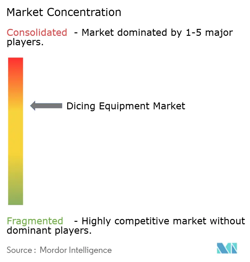
| Market Concentration | Medium |
Major Players *Disclaimer: Major Players sorted in no particular order Image © Mordor Intelligence. Reuse requires attribution under CC BY 4.0. | |
Dicing Equipment Market Analysis by Mordor Intelligence
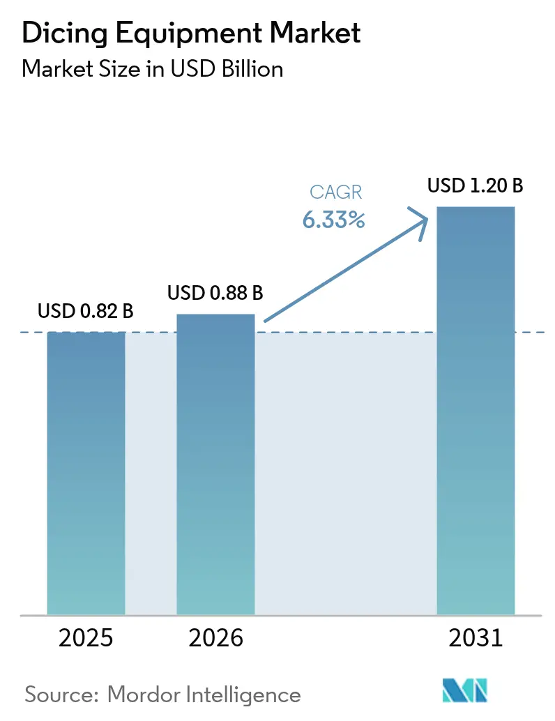
The Dicing Equipment Market size is projected to be USD 0.82 billion in 2025, USD 0.88 billion in 2026, and reach USD 1.20 billion by 2031, growing at a CAGR of 6.33% from 2026 to 2031.
Continued migration toward advanced wafer-level packaging, wider adoption of plasma- and stealth-based singulation, and geographically diversified fab construction underpin this growth trajectory. Equipment suppliers benefit from larger 300 mm substrate runs and the proliferation of wide-bandgap power devices, while service-oriented revenue streams from blade replacement and process optimization partially buffer cyclical slowdowns. Competitive pressure stays acute as Chinese toolmakers win government subsidies and target mature nodes, even as Japanese incumbents defend share through global service footprints and robust patent portfolios. Rising compliance costs linked to slurry disposal and rare-earth supply risk temper near-term margins but also accelerate the shift to low-consumable plasma processes that promise leaner operating outlays.
Key Report Takeaways
- By dicing technology, blade dicing held 52.43% of the 2025 dicing equipment market share, while plasma dicing is forecast to register the fastest 7.17% CAGR through 2031.
- By wafer size, the 200 mm segment captured 42.23% of the 2025 dicing equipment market, whereas 300 mm platforms are projected to grow at a 7.07% CAGR through 2031.
- By application, memory and logic produced 37.21% of 2025 revenue, and power devices are expected to expand at a 7.41% CAGR over 2026-2031.
- By end-user, foundries commanded 44.43% of 2025 demand, and outsourced assembly and test providers are predicted to grow at a 6.94% CAGR to 2031.
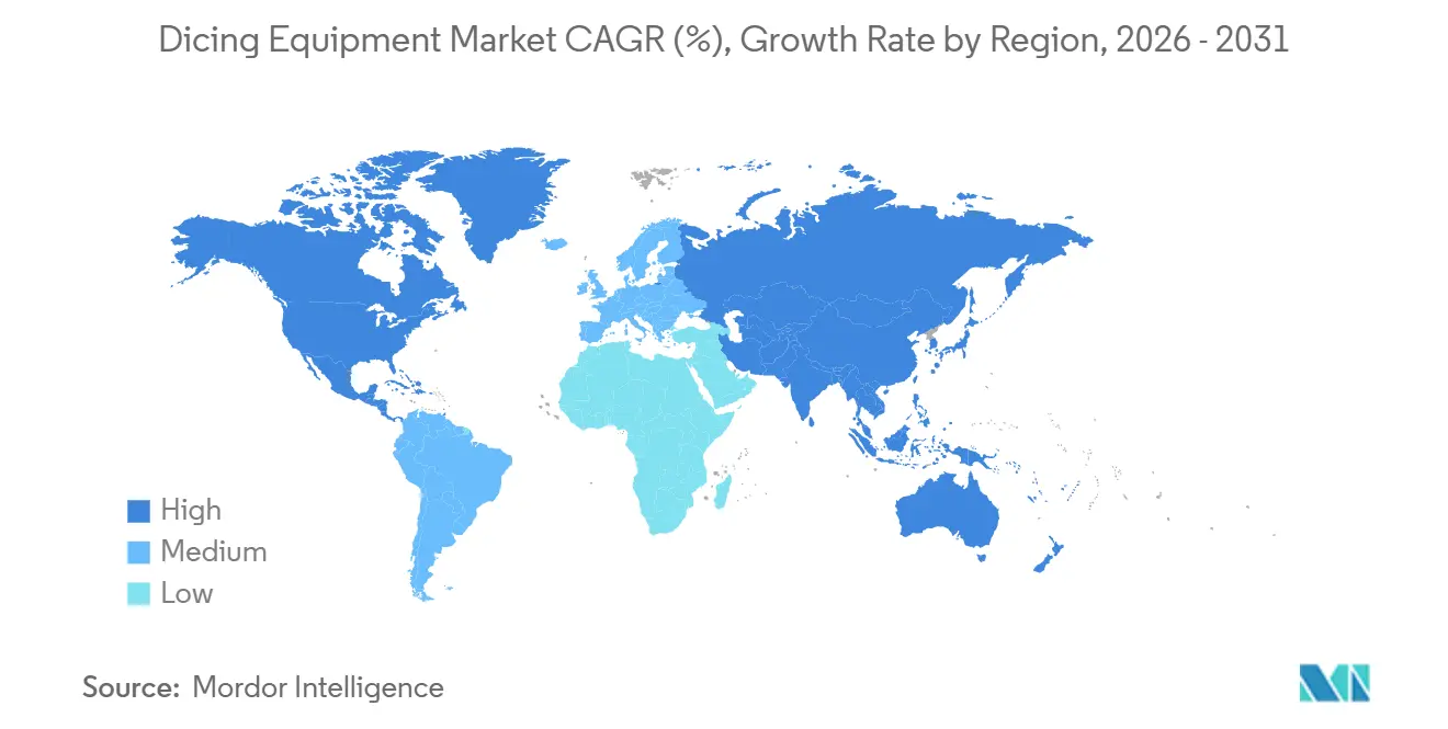
- By geography, Asia-Pacific accounted for 56.57% of 2025 sales, and the Middle East is set to log the quickest 7.31% CAGR through 2031.
Note: Market size and forecast figures in this report are generated using Mordor Intelligence’s proprietary estimation framework, updated with the latest available data and insights as of 2026.
Global Dicing Equipment Market Trends and Insights
Drivers Impact Analysis*
| Driver | (~) % Impact on CAGR Forecast | Geographic Relevance | Impact Timeline |
|---|---|---|---|
| Technological Advancements in High-Precision Motion Systems | +0.8% | Global, early uptake in Japan and Taiwan | Medium term (2-4 years) |
| Surge in Demand from Advanced Logic and Memory Fabs | +1.2% | Asia-Pacific core, spill-over to North America and Middle East | Short term (≤ 2 years) |
| Rapid Adoption of 3D Packaging and Heterogeneous Integration | +1.0% | Global, concentrated in Taiwan, South Korea, and United States | Medium term (2-4 years) |
| Growing Deployment of Power Devices for Electric Vehicles and Renewables | +0.9% | Global, strongest uptake in China, Europe, and North America | Long term (≥ 4 years) |
| Shift Toward Plasma Dicing for Ultra-Thin Wafers | +0.7% | Asia-Pacific and Europe, advanced packaging hubs | Medium term (2-4 years) |
| Localization Incentives for Domestic Equipment in China | +0.6% | China, with secondary effects in Southeast Asia | Short term (≤ 2 years) |
| Source: Mordor Intelligence | |||
Technological Advancements in High-Precision Motion Systems
Modern blade saws now integrate air-bearing spindles and piezo-actuated stages, pushing positioning tolerance below 1 µm and reducing chipping at the die edge by up to 40% on 300 mm substrates [1]DISCO Corporation, “DFD6362 Blade Saw Spec Sheet,” disco.co.jp. Linear-motor indexing further shortens cycle time, enabling throughputs exceeding 1,200 dies per hour on heavily thinned wafers [2]Accretech, “AD3500 Linear Stage Introduction,” accretech.jp. These upgrades arrive just as the IEEE roadmap calls for die thicknesses under 30 µm for high-bandwidth memory stacks, sharpening demand for vibration-free motion systems. Japan and Taiwan fabs adopt early because hybrid-bonding yields deteriorate rapidly when micro-cracks propagate, and local tool suppliers already operate dense service networks to support 24-hour operations. As new fabs in the Middle East evaluate baseline process flows, vendors that emphasize sub-micrometer run-out are well positioned to secure anchor orders.
Surge in Demand from Advanced Logic and Memory Fabs
The combined 2025-2026 capital budgets of TSMC, SK Hynix, and Micron exceed USD 90 billion, with large allocations toward high-bandwidth memory and 2 nm logic nodes that each require 3-4 additional dicers per incremental 10 k-wpm capacity. Equipment pull-ins concentrate in Taiwan and South Korea, but pilot discussions with Gulf investors suggest a 5-7% re-routing of orders once export-control clearances emerge. Memory fabs moving to 12-16 layer vertical stacks now favor plasma or stealth methods to avoid thermal shock, reinforcing upselling opportunities for premium etch-based systems. Short procurement cycles magnify the CAGR impact because fabs schedule tool deliveries one quarter before wafer-start ramps, accelerating revenue realization for suppliers adept at quick lead-time fulfillment.
Rapid Adoption of 3D Packaging and Heterogeneous Integration
Chiplet-based layouts complicate singulation, as each die material, thickness, and backside metallization requires unique blade grit and feed profiles to avert delamination. The 2024 IEEE roadmap projects that chiplets will account for more than 30% of high-performance compute shipments by 2028, tripling their 2024 share. Contract packaging house ASE responded by lifting 2025 capex by more than 60% and adding Malaysian fan-out lines that use stealth dicing to deliver narrow 10 µm streets without residue. Panasonic’s hybrid laser-cleave approach reduces total cycle time by 35% for ultra-thin silicon-on-insulator wafers [3]SPTS Technologies, “Sigma fxP Plasma Dicer Performance,” spts.com. As logic vendors co-package analog and memory tiles, equipment capable of recipe switching within seconds becomes indispensable, making software-rich platforms a gating factor for high-mix production.
Growing Deployment of Power Devices for Electric Vehicles and Renewables
Silicon carbide wafer shipments climbed 40% in 2025 as automakers embraced 800 V drivetrains that require higher blocking voltages. Plasma dicing eliminates mechanical stress on gallium nitride devices, preserving heterojunction integrity and keeping edge-defect density below 5 /cm on 200 mm wafers. Because power-device gross margins can run 10-15 points higher than logic chips, fabs willingly pay a USD 0.06-0.10 premium per cut to avoid scrap. Edge-contactless singulation also allows thinner sawn edges, increasing usable die per wafer and offsetting high substrate costs. Policy-backed solar and wind build-outs in China, Europe, and North America sustain multi-year demand for high-temperature power dies, extending tool order visibility beyond normal three-quarter horizons.
Restraints Impact Analysis*
| Restraint | (~) % Impact on CAGR Forecast | Geographic Relevance | Impact Timeline |
|---|---|---|---|
| High Capital Expenditure and Long Payback Period | -0.9% | Global, most acute in emerging fab regions | Medium term (2-4 years) |
| Yield Losses from Chipping and Micro-Cracks | -0.7% | Global, concentrated in wide-bandgap and ultra-thin work | Short term (≤ 2 years) |
| Stricter Slurry and Chemical Disposal Regulations | -0.4% | North America and Europe, spill-over to Asia-Pacific | Long term (≥ 4 years) |
| Laser Source Supply Bottlenecks and Rare-Earth Dependency | -0.5% | Global, most severe in North America and Europe | Medium term (2-4 years) |
| Source: Mordor Intelligence | |||
High Capital Expenditure and Long Payback Period
Plasma dicers list for USD 3-4 million versus USD 1.5-2 million for advanced blade saws, stretching cash flows for outsourced assembly and test providers that operate on 8-12% operating margins. Deferred-payment terms now average 18 months, yet payback still exceeds four years when line utilization dips below 70%. Smaller Southeast Asian facilities often resort to leasing, paying interest spreads 200-300 bps above prime, a hurdle that slows equipment refresh even when technology obsolescence presses. New Middle Eastern fabs carry sovereign guarantees, but until wafer starts stabilize lenders remain cautious, delaying conversion of memoranda of understanding into firm purchase orders.
Yield Losses from Chipping and Micro-Cracks
A 2025 Journal of Electronic Materials study found that 5 µm-deep microcracks reduced die strength by 40% and doubled field-failure incidence in automotive modules [4]Journal of Electronic Materials Editorial Board, “Micro-Crack Impact on Power Module Reliability,” link.springer.com. Silicon carbide’s Mohs hardness of 9 accelerates blade wear, pushing consumable costs 30-40% higher than on silicon. Plasma etching lowers chipping to near zero but introduces sidewall roughness above 1 µm unless post-etch cleaning extends cycle time by 10-15%. Because outsourced assembly and test providers typically absorb dicing scrap, even a 200-300 bp yield hit erodes thin single-digit net margins, discouraging fast adoption of riskier yet cheaper third-party blade suppliers.
*Our forecasts treat driver/restraint impacts as directional, not additive. The impact forecasts reflect baseline growth, mix effects, and variable interactions.
Segment Analysis
By Dicing Technology: Plasma Gains as Thickness Shrinks
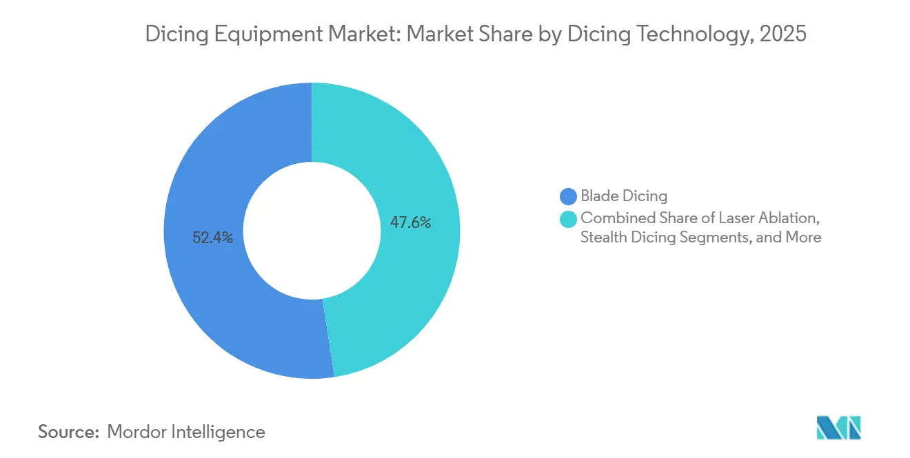
Blade systems generated 52.43% of 2025 revenue as their mature cost-per-cut of under USD 0.02 remains compelling for dies thicker than 75 µm. Plasma dicing is forecast to advance at a 7.17% CAGR, aligned with high-bandwidth memory and CMOS image sensor lines that now ship wafers thinned to 20 µm, where kerf loss from blades becomes unacceptable. The dicing equipment market size for plasma tools is projected to outpace overall growth as fabs migrate toward non-contact singulation to meet hybrid bonding defect tolerances. Stealth dicing gains a niche in silicon-on-insulator and GaAs substrates thanks to 10 µm street widths, but laser ablation remains limited to sapphire LED lines due to thermal-stress control issues.
Vendors counter plasma’s advance by deploying 15 µm-thick blades spinning at 60,000 rpm, though spindle deflection physics cap further gains. SPTS demonstrated 0.3 µm sidewall variation via fluorine-argon co-flow, nearing hybrid bonding requirements and underscoring process parameter tuning as a differentiator. Hybrid laser-plasma cells under co-development in Japan suggest that future platforms may merge speed and edge quality, providing an upgrade path for current blade-saw users. Taken together, the dicing equipment market continues to bifurcate between high-volume low-mix lines that stay with blades and performance-critical lines that justify the premium of plasma or stealth systems.


By Wafer Size: 300 mm Pulls Ahead
The 200 mm tranche retained 42.23% of 2025 spend, reflecting entrenched analog and power-device fabs that leverage fully depreciated tools. The 300 mm tier, however, is forecast to log a 7.07% CAGR as the only economically viable substrate for leading-edge logic and high-bandwidth memory, effectively becoming the default size for new greenfield projects. TSMC and Samsung collectively capped 2025 investment above USD 60 billion, and every new process node introduction at their sites mandates an additional 300 mm dicers, giving the dicing equipment market share for that diameter an upward trajectory.
Advanced packaging trends further reinforce 300 mm dominance, as multiple dicing passes split a single interposer wafer into logic, memory, and passive tiles. Equipment makers now sell dual-spindle platforms capable of parallel cutting, trimming cycle time by 40% compared with single-spindle predecessors, a feature that appeals to outsourced assembly and test providers chasing hourly wafer-throughput benchmarks. 150 mm and below will decline structurally as compound-semiconductor vendors transition to 200 mm lines, shrinking legacy platform demand, though ensuring a long tail of replacement consumables.
By Application: Power Devices Outpace Logic
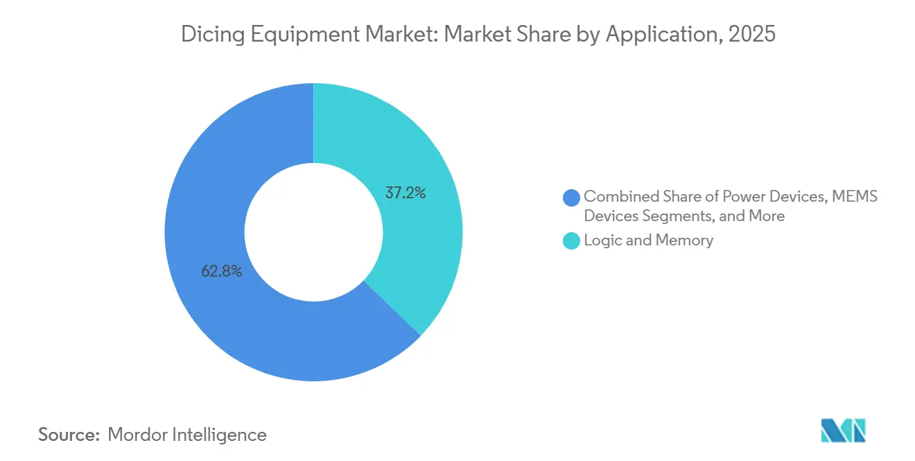
Memory and logic accounted for 37.21% of 2025 sales, but power devices, buoyed by electric vehicle inverter and renewable inverter builds, are set to pace the field with a 7.41% CAGR through 2031. Each battery-electric vehicle integrates 300-500 silicon carbide dies, and photovoltaic optimizers pack 50-100 gallium nitride dies per kilowatt, providing a stable pull for edge-defect-sensitive plasma platforms. The dicing equipment market size allocated to power devices thus grows faster than total spending, even as legacy blade solutions cling to mainstream logic wafers, where die thickness remains above 50 µm.
CMOS image sensors remain a steady mid-single-digit growth pocket as OEMs raise pixel counts, necessitating vibration-free cutting to avoid pixel hot spots. MEMS shares inch higher in automotive and industrial IoT, while RFID and smart card demand mature, collectively retarding volume growth. Across categories, suppliers that can embed machine vision to auto-tune spindle speed in response to real-time edge data will capture wallet share because they directly lift final-test yield
By End-User Industry: OSATs Gain Share
Foundries accounted for 44.43% of 2025 outlays, driven by capital programs at TSMC, Samsung, and Intel. Outsourced assembly and test providers, however, are projected to expand at a 6.94% CAGR as more integrated device manufacturers outsource heterogeneous integration to lower fixed costs. The dicing equipment market size attributable to OSATs grows accordingly, especially in Southeast Asia, where high-throughput multi-spindle blades suit cost-per-die targets. ASE’s 2025 Malaysian addition and KYEC’s Singapore upgrade exemplify capacity bets aimed at automotive and high-performance compute workflows.
Foundry campuses still purchase ultra-precision dicers for sub-2 nm nodes because cycle-time synchronization across lithography and backside power redistribution demands tight in-house integration. Meanwhile, OSATs win mid-tier logic, MEMS, and gallium nitride business by bundling test and packaging, an offer vertically integrated fabs cannot match on price. This dichotomy splits procurement into premium accuracy tools versus high-uptime fleet dicers, compelling vendors to support both specification extremes within the same product families.
Geography Analysis
Asia-Pacific accounted for 56.57% of 2025 revenue, and within the region, Taiwan, South Korea, and China remain the linchpins. Construction of SK Hynix’s M15X line and Yongin mega-fab will add more than 400 k-wpm of high-bandwidth memory capacity between 2026-2027, each requiring three to four dicers per 10 k-wpm tranche. TSMC’s multibillion-dollar Arizona and 2 nm ramp orders keep Japanese blade suppliers’ assembly lines saturated, while Chinese subsidy-fueled toolmakers offer 40-50% price discounts to domestic fabs under 25% import tariffs.
North America and Europe accounted for roughly one-quarter of 2025 purchases, energized by Intel’s USD 25 billion outlay for Ohio and Arizona capacity, as well as Micron’s cross-Pacific high-bandwidth memory spend. Both regions enforce stricter chemical-disposal rules, which inflate operating costs but also steer buyers toward plasma systems that consume no coolant water. Financial incentives under the EU Chips Act aim for a 20% global semiconductor output share by 2030, an ambition that translates into rising dicing tool penetration once German and Italian fabs break ground.
The Middle East registers the fastest 7.31% CAGR through 2031. Saudi Arabia’s Public Investment Fund and the United Arab Emirates both court leading-edge partners, dangling more than USD 140 billion in combined incentives. Although technology transfer hurdles mean first silicon likely slips to 2028-2029, vendors without local service hubs are already scouting Dubai and Riyadh for field-support bases. If even one gigafab proceeds, regional demand could absorb 5-7% of global dicing shipments, shifting the commercial center of gravity away from traditional Northeast Asian strongholds.

Regulatory Landscape
Cross-border sales of dicing, stealth, laser, and plasma singulation tools increasingly come under export-control and trade-policy scrutiny because they are part of the semiconductor manufacturing equipment stack used for advanced logic, memory, and packaging. In January 2025, the US Bureau of Industry and Security (BIS) issued an interim final rule that added due-diligence expectations for front-end fabricators and OSATs handling advanced ICs, raising documentation and screening requirements that can extend procurement and service workflows for tool OEMs and their channel partners. Separately, a January 2026 US Section 232 action implemented a 25% ad valorem tariff on certain advanced semiconductors and derivative products, while explicitly excluding semiconductor manufacturing equipment for domestic US production. That carve-out creates a practical distinction between equipment supporting US buildouts and supply chains tied to restricted destinations.
Outside of government measures, equipment qualification is shaped by standards embedded in fab purchasing contracts. SEMI standards (for example, SEMI S2/S8/S22 and related equipment safety and environmental requirements) operate as de facto mandatory acceptance criteria for tool installation and ongoing operation, while cybersecurity expectations are tightening as fabs align internal controls with the NIST Cybersecurity Framework 2.0 and related semiconductor manufacturing profiles. As a result, dicing equipment vendors increasingly link performance claims (kerf, chipping, sidewall quality) with auditable compliance for safety, environmental requirements, and security-by-design, helping them maintain approved vendor status at leading fabs and OSATs.
Value Chain Analysis
The dicing equipment value chain begins with precision subsystems such as air-bearing or high-speed spindles, linear motors and stages, metrology and machine vision, laser sources for stealth/ablation, RF power and vacuum components for plasma, and specialty materials such as diamond blades and process consumables. It then extends through tool design, integration, factory acceptance testing, and field installation at fabs and OSATs. Ongoing revenue is supported by consumables and services, including blade replacement, process recipes, uptime programs, and yield optimization, which are especially relevant for high-mix production and for demanding substrates such as ultra-thin silicon and wide-bandgap wafers.
Demand is concentrated among foundries, IDMs, and OSATs that ramp advanced packaging and memory/logic output, where singulation quality affects final yield and reliability. Supplier structure remains concentrated in blade dicing, with DISCO and Tokyo Seimitsu (ACCRETECH) holding a dominant installed base that influences preferences for spares, qualification data, and service coverage. This concentration can become a chokepoint for high-volume programs, including HBM and CoWoS-type workflows, and it increases the value of localized service hubs, certified third-party parts, and hybrid fleets that combine blade, stealth/laser, and plasma approaches. Together, these options help meet street-width and die-strength requirements across applications.
Competitive Landscape
DISCO and Tokyo Seimitsu anchor the blade segment with more than 60% of shipments, a dominance built on a formidable patent portfolio spanning spindle metallurgy, coolant delivery, and process monitoring. Their pricing resilience is evident in DISCO’s FY 2025 first-half operating income of JPY 66.4 billion (USD 460 million), which highlights the company’s ability to withstand tariff pressures from China. This entrenched position underscores how intellectual property and process know-how remain decisive in sustaining margins in a concentrated market.
By contrast, plasma dicing niches are more fragmented, with players like SPTS, Plasma-Therm, and 3D-Micromac competing on sidewall quality. SPTS, for instance, has demonstrated 0.3 µm roughness using fluorine-argon chemistries, a benchmark that appeals to advanced packaging lines. Western challengers are also pushing boundaries with software-defined blades and real-time vision feedback, exemplified by a 2025 USPTO filing that introduced torque modulation every 50 ms, reducing silicon carbide chipping by 35%. These innovations highlight how process control and adaptive tooling are becoming differentiators in plasma and hybrid approaches.
Chinese entrants such as Han’s Laser and Suzhou Delphi Laser leverage heavy subsidies, CNY 1.5 billion (USD 210 million), to slash list prices by 40–50%. Yet, their spindle run-out remains two to three times higher than Japanese norms, limiting adoption in hybrid-bonding lines where precision is critical. Meanwhile, Japanese firms are experimenting with hybrid plasma-stealth prototypes that promise 30% cycle-time reductions, though the USD 50 million project costs necessitate anchor customers to share risk. Across all segments, compliance with SEMI S2, ISO 9001, and ISO 14001 remains a gating factor, conferring trust premiums especially for fabs tied to automotive functional-safety audits.
Dicing Equipment Industry Leaders
DISCO Corporation
Advanced Dicing Technologies Ltd.
Plasma-Therm LLC
Tokyo Seimitsu Co., Ltd. (ACCRETECH)
Panasonic Connect Co., Ltd.
- *Disclaimer: Major Players sorted in no particular order

Market Opportunities and Future Outlook
Advanced packaging and heterogeneous integration are expanding the addressable scope for non-contact singulation, particularly where hybrid bonding and ultra-thin wafers make particulate, micro-cracks, and thermal damage more consequential. The shift toward dry or low-contamination processes (stealth dicing, laser approaches, and plasma dicing) creates room for platforms that can switch recipes quickly across mixed materials and backside metallization, while still meeting procurement-gating requirements such as SEMI safety and environmental standards. Cybersecurity expectations are also a differentiator, as fabs continue to align checklists with NIST-aligned frameworks.
Capacity and process transitions visible in 2026 activity point to near-term entry points for tool and service suppliers beyond traditional Northeast Asian hubs. Tower Semiconductor announced a Japan expansion track tied to 300 mm silicon photonics and advanced packaging, supported by a USD 1 billion grant package, which underwrites incremental demand for high-precision singulation as 300 mm packaging lines broaden. Okmetic began volume production at the expanded Vantaa facility in Finland, increasing 200 mm polished wafer capacity for MEMS, sensor, RF, and power device uses, reinforcing demand for dicing solutions designed to protect fragile structures and maintain tight edge-defect control. Alongside these capacity moves, increasing emphasis on equipment energy efficiency and compliance-ready designs, particularly in Japan and Europe, supports opportunities for OEMs that can quantify lower consumables, reduced wastewater burden, and improved tool-level power management without trading off throughput.
Recent Industry Developments
- February 2026: DISCO Corporation set the construction start for its new Gohara Plant in Kure City, Hiroshima, with a planned investment of JPY 33 billion to strengthen production efficiency and resilience for precision processing tools. The added manufacturing footprint supports higher output and business continuity for dicing and related back-end equipment, a key constraint when leading fabs and OSATs pull in delivery schedules.
- January 2026: Plasma-Therm announced a collaboration with Elevate Quantum and QPICs, Inc. to deploy the CORIAL plasma processing platform within a Quantum Fab infrastructure in Colorado. The collaboration places Plasma-Therm closer to emerging photonics and quantum manufacturing process flows that use plasma-based steps alongside singulation, expanding adjacency demand for compatible back-end processing capability.
- April 2025: DISCO Corporation announced a corporate update focused on strengthening its operational base for precision processing equipment and services. Actions tied to manufacturing and support readiness reinforce the company's ability to meet tight uptime and qualification expectations from high-volume semiconductor customers that depend on stable spare parts and service response.


Research Methodology Framework and Report Scope
Market Definition and Coverage
We define the dicing equipment market as revenue from tools and systems used to singulate wafers and similar substrates into individual dies, including blade and advanced dicing methods used in semiconductor device manufacturing.
Scope exclusions: We exclude upstream wafer fabrication tools (like lithography and deposition) and downstream assembly and test tools unless the spend is directly tied to the dicing step.
Segmentation Overview
- By Dicing Technology
- Blade Dicing
- Laser Ablation
- Stealth Dicing
- Plasma Dicing
- By Wafer Size
- Less than equal to 150 mm
- 200 mm
- 300 mm
- Greater than 450 mm
- By Application
- Logic and Memory
- MEMS Devices
- Power Devices
- CMOS Image Sensors
- RFID / Smart Cards
- By End-User Industry
- Foundries
- IDMs
- OSATs
- By Geography
- North America
- United States
- Canada
- Mexico
- South America
- Brazil
- Argentina
- Rest of South America
- Europe
- Germany
- United Kingdom
- France
- Italy
- Spain
- Russia
- Rest of Europe
- Asia-Pacific
- China
- Japan
- India
- South Korea
- South-East Asia
- Rest of Asia-Pacific
- Middle East
- Saudi Arabia
- United Arab Emirates
- Rest of Middle East
- Africa
- South Africa
- Egypt
- Rest of Africa
- North America
Data Sources, Market Sizing, and Validation
Desk Research
Desk research was used to set the basic demand picture and to avoid building the model on one single data point. We reviewed public semiconductor and electronics indicators that connect closely to dicing demand, such as wafer starts, fab utilization signals, packaging throughput cues, and shifts toward advanced nodes and new materials.
Sources used were mainly public and repeatable, such as SEMI publications, World Semiconductor Trade Statistics (WSTS), the US International Trade Commission trade data, UN Comtrade, and technical literature from IEEE and similar peer-reviewed outlets. We also used annual reports, investor presentations, and press releases to understand product launches and capacity moves, then cross-checked the trends using paid subscriptions for company financials, patent databases, and an import-export shipment level database when it helped resolve gaps. These examples are not exhaustive, and many other public sources were referenced for data collection, validation, and clarification during the work.
Primary Interviews and Surveys
Primary work was used to pressure-test assumptions that are hard to read from public data, especially technology mix shifts and pricing behavior across blade, stealth, laser, and plasma systems. We spoke with a balanced mix of equipment-side and customer-side participants, including manufacturing, process, and procurement roles across major wafer and packaging regions, so that regional mix and use-case differences were captured before finalizing the model.
Distribution of primary research fieldwork respondents
| Company type | Respondent position | Region |
|---|---|---|
| Top tier: 39% | CXOs: 14% | APAC: 47% |
| Mid tier: 44% | Functional/Unit leaders: 32% | EMEA: 35% |
| Smaller Players: 17% | Managers: 54% | Americas: 18% |
Market-Sizing & Forecasting
Sizing starts with a top-down build where wafer demand indicators and device output trends are translated into an addressable dicing equipment spend pool by applying adoption and replacement rhythms across key dicing technologies. Once that pool is formed, it is corroborated through selective bottom-up approximations, including supplier revenue roll-ups, sampled system ASP ranges, and channel checks for shipment momentum, then used to tune the totals.
Inputs used in the model include, for example, wafer diameter mix (200 mm versus 300 mm), the share of demand from logic and memory versus power devices and MEMS, the penetration of advanced dicing methods, average tool ASP movement by technology, and the timing of new fab and OSAT capacity additions. When information was missing for smaller markets or niche applications, we used proxy relationships (such as wafer start direction and capex cycles) and then confirmed reasonableness through interviews.
For forecasting, scenario analysis was applied around semiconductor capex cycles, node transitions, and mix shifts to new materials, followed by an annualized smoothing step to avoid overreacting to short-term order swings. Assumptions were adjusted only when multiple signals aligned, including primary feedback, public capex guidance, and observable demand indicators.
Data Validation & Update Cycle
Outputs are checked through more than one lens, so the total market value must reconcile with independent signals such as semiconductor capex direction, wafer throughput trends, and disclosed equipment performance updates. Outliers are flagged early, and we re-check the underlying drivers, including technology mix, regional weighting, and ASP assumptions, before results move to internal review.
A multi-step review is followed so that calculation logic, year alignment, and currency conversions stay consistent across the model. Reports are refreshed annually, and interim updates are done when material events occur, such as major capex revisions or sharp demand resets. Before delivery, a fresh pass is completed so clients receive the latest updated view based on newly available public information.
Mordor Intelligence's Dicing Equipment Market Size Measured Against Other Published Estimates
Published market numbers for dicing equipment often do not line up because the counted spend can quietly shift from pure dicing tools to broader wafer processing toolsets, and because the base year and currency timing are not always treated the same way.
Some estimates roll in thin wafer processing steps and adjacent singulation related services into one total, then push optimistic replacement cycles through the forecast. For Mordor Intelligence, only equipment revenue tied directly to the wafer and substrate dicing step is counted, and technology mix and ASP progression are refreshed using checks such as wafer diameter mix and foundry and OSAT capacity ramps.
Benchmark comparison
| Source | Market Size | Gaps in Research Methodology |
|---|---|---|
| Mordor Intelligence | USD 0.88 B (2026) | |
| Global Consultancy A | USD 1.83 B (2024) | Uses an earlier base year and appears to include a wider tool set around wafer singulation and related processing, which lifts the spend pool beyond dicing equipment only. |
| Industry Publisher B | USD 0.80 B (2025) | Focuses on automatic wafer dicing equipment and typically narrows product coverage, and it can also understate totals when non-automatic systems and newer dicing technologies are not fully captured. |
The table shows that the spread mainly comes from scope and year alignment choices, not from small math differences. By keeping the spend pool tied to dicing equipment only, then validating mix and pricing with repeatable signals and expert checks, the estimate stays traceable to a clear demand base and can be updated in a consistent way year after year.


Key Questions Answered in the Report
How fast is demand for dicing tools expected to grow between 2026 and 2031?
Total spending is projected to rise at a 6.33% CAGR, taking the dicing equipment market from USD 0.88 billion in 2026 to USD 1.20 billion by 2031.
Which wafer size will generate the largest incremental equipment need?
300 mm lines will see the fastest 7.07% CAGR as leading-edge logic and memory migrate exclusively to that diameter.
Why is plasma dicing gaining traction over blade systems?
Plasma eliminates mechanical stress, cuts kerf loss, and supports die thickness below 25 µm, all of which are essential for high-bandwidth memory and chiplet packages.
What factors limit wider adoption of stealth or plasma tools?
Up-front prices of USD 3-4 million, payback periods beyond four years at <70% utilization, and additional sidewall cleaning steps dampen near-term uptake.
Which region shows the highest growth potential for equipment vendors?
The Middle East is forecast to expand at 7.31% CAGR as sovereign-backed gigafab projects in the United Arab Emirates and Saudi Arabia progress.
How concentrated is supplier power in the current market?
Two Japanese firms hold >60% of blade shipments, giving the industry a moderate concentration score of 7 on a 1-10 scale.
Page last updated on: