Semiconductor CVD Market Size
| Study Period | 2019 - 2029 |
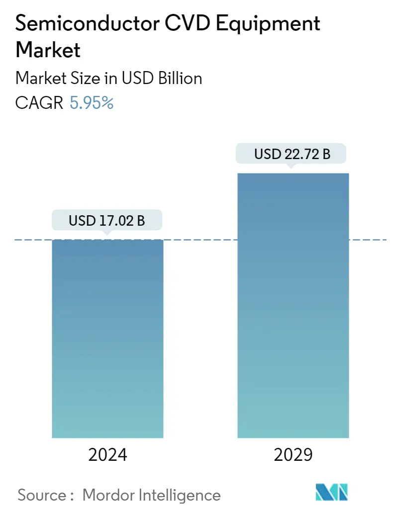
| Market Size (2024) | USD 17.02 Billion |
| Market Size (2029) | USD 22.72 Billion |
| CAGR (2024 - 2029) | 5.95 % |
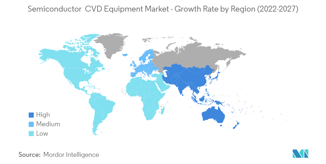
| Fastest Growing Market | Asia Pacific |
| Largest Market | Asia Pacific |
Major Players
*Disclaimer: Major Players sorted in no particular order |
Need a report that reflects how COVID-19 has impacted this market and its growth?
Semiconductor CVD Market Analysis
The Semiconductor CVD Equipment Market size is estimated at USD 17.02 billion in 2024, and is expected to reach USD 22.72 billion by 2029, growing at a CAGR of 5.95% during the forecast period (2024-2029).
Increasing demand for microelectronics-based consumer products, resulting in the faster growth of the semiconductor, LED, and storage device industry and strict regulations on the use of Cr6 for electroplating are primarily driving the growth of the CVD equipment market.
- The Chemical Vapor Deposition (CVD) process is often used in manufacturing semiconductors and producing thin films. In recent years, CVD synthesis has reached new heights with the precise manufacturing of both inorganic thin films of 2D materials and high-purity polymeric thin films that may be conformally deposited on various substrates.
- Precursor gases (typically diluted in carrier gases) are supplied into the reaction chamber at around ambient temperatures in semiconductor chemical vapor deposition equipment. They react or break down when they pass across or come into touch with a heated substrate, generating a solid phase that is deposited on the substrate. The temperature of the substrate is important because it can influence the reactions that occur.
- CVD is widely used in microfabrication techniques to deposit materials in various morphologies, including polycrystalline, monocrystalline, amorphous, and epitaxial. Silicon (dioxide, carbide, nitride, oxynitride), carbon (fiber, nanofibers, nanotubes, diamond, and graphene), fluorocarbons, filaments, tungsten, titanium nitride, and a variety of high-k dielectrics are among these materials.
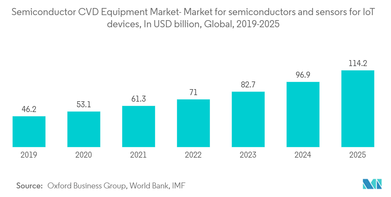
- Governments and business stakeholders are watching developments in the microelectronics industry closely because these technologies have the potential to disrupt and propel the Internet of Things market. Due to the increased adoption of virtual reality and augmented reality gadgets, R&D for microelectronics may also increase in response to the looming bandwidth constraint.
- They are making semiconductors. CVD setup can be complex and comes with huge costs. The foundries and Outsources Semiconductor Assembly and Test (OSAT) companies are likely to face increased pressure on capital expenditures as they continue to expand production to address the rising chip demand.
- The COVID -19 outbreak affected the overall semiconductor and chip fabrication market from the demand and supply sides. The nationwide lockdowns and closure of semiconductor plants have further fueled the supply shortage trend. However, these effects are likely to be short-term and temporarily affect the demand for CVD technologies. Moreover, government precautions globally to support automotive and industrial sectors could help revive foundry industry growth.
Semiconductor CVD Market Trends
This section covers the major market trends shaping the Semiconductor Chemical Vapor Deposition Equipment Market according to our research experts:
Increase in Demand for Microelectronics and Consumer Electronics to Fuel the Demand
- The rise in microelectronics and consumer electronics sales is expected to drive the demand for semiconductor ICs over the forecasted period. However, the demand for semiconductor ICs is expected to increase the production capacity of semiconductor device manufacturers, which may augment the demand in the chemical vapor deposition market.
- The integrated device manufacturer (IDM) includes logic, optoelectronics, sensors, discrete components, and others. (Excluding Memory Manufacturers). An integrated device manufacturer manufactures and sells integrated circuits (ICs). A classic IDM owns its branded chips, designs them in-house, and makes them in a fabrication factory. IDMs pursue node scaling beyond 10 nm to 5 nm and even 3 nm, while other manufacturers renounce planar architectures favoring sophisticated, three-dimensional (3D) structures for logic and memory.
- Thin-film deposition is a vital step in manufacturing integrated circuits (ICs). The most common approach for thin-film growth is CVD. Precursors and reactants are combined in a process chamber before being delivered in a steady state to form a film on the wafer in CVD.
- The market is witnessing the presence of various IDMS undertaking different initiatives to gain a competitive advantage. For instance, the Canadian Photonics Fabrication Centre (CPFC) is a facility that provides fabrication services, pre-commercial photonic devices, and photonic integrated circuit manufacturers. Design and modeling, epitaxy, fabrication, and test and characterization are among the fee-based services provided by CPFC. CPFC operates a metal-organic chemical vapor deposition (MOCVD) reactor for the research and fabrication of gallium arsenide (GaAs) and indium phosphide (InP)-based devices.
- Also, governments and industry stakeholders are keenly following the advances in the microelectronics industry as these technologies might potentially disrupt and boost the Internet of Things market. R&D for microelectronics may also increase with the impending bandwidth crunch due to the improved penetration of virtual reality and augmented reality devices. In September 2021, the government organized a conference with 50 European and international semiconductor industry representatives to persuade them to invest in Germany by offering them a help package. The German government plans to spend roughly USD 4.5 billion to recapture manufacturing locations across the semiconductor value chain.
Asia Pacific as the Most Lucrative Market for Global Semiconductor CVD Equipment
- The Asia Pacific is a potential region with various manufacturing facilities for developing consumer electronics and semiconductor-related products. The particular region is expected to occupy the largest market share in the semiconductor CVD equipment market in the coming years.
- The advancement of the electronics and semiconductor industries, particularly in China, is driving market expansion in the region. In growing economies like China and India, the expansion in industrialization and the number of end-user sectors and companies presented enormous undiscovered potential. Due to the sheer existence of growing economies and the development of the electronics industries, the region is predicted to propel at a significant rate over the forecast period.
- China has a very ambitious semiconductor agenda. Backed by USD 150 billion in funding, the country is developing its domestic IC industry and plans to make more of its chips. Greater China, which encompasses Hong Kong, China, and Taiwan, is a geopolitical hotspot. The US-China trade war is compounding tensions in an area where all the leading process technology is located, forcing many Chinese companies to invest in their semiconductor foundries.
- The rapid expansion of the APAC automotive semiconductor industry is expected to be fueled by the rising demand for electric vehicles. Automobile manufacturers must continue to innovate, create, and develop self-driving cars, which have already attracted many customers in key automotive manufacturing countries.
- India has emerged as one of the world's fastest-growing economies due to its large population. According to projections, the automotive semiconductor market in the country will increase rapidly in the coming years. The Automotive industry is complemented by a strong semiconductor R&D infrastructure, which will open new potential for the semiconductor etch market in India in the forthcoming years.
Semiconductor CVD Industry Overview
The market is fragmented with high competitive rivalry. Also, owing to their market penetration and the ability to offer advanced products, the competitive rivalry is expected to be high. Although the market comprises various players, only a handful are prominent in the market for their high standards and excellent quality.
- August 2021 - CVD Equipment Corporation, one of the key suppliers of chemical vapor deposition systems, announced that it had secured a production system order worth about USD 1.7 million from a large US-based electric car battery material producer. In the first quarter of 2022, the system will be delivered to the customer.
- July 2021 - ASM International N.V. announced the availability of Intrepid ESATM epitaxy equipment for 300mm applications in power and analog devices and epitaxial silicon wafers. The new ESA tool increases ASM's atmospheric epi capabilities with ASM's first 300mm atmospheric cluster tool based on the proven, high-volume manufacturing Intrepid platform. On-wafer performance with the Intrepid ESA.
Semiconductor CVD Market Leaders
AIXTRON SE
ASM International
CVD Equipment Corporation
Applied Materials, Inc
Oxford Instruments
*Disclaimer: Major Players sorted in no particular order
Semiconductor CVD Market News
- September 2021 - Lam Research announced the expansion of its manufacturing footprint in Oregon with a new 45,000 square foot facility in Sherwood. The new facility is Lam's fifth manufacturing site in the United States. It will further enhance its resilience and ability to meet increasing customer demand as chip suppliers seek to scale up production.
- February 2021 - Oxford Instruments Plasma Technology announced that it would relocate to a state-of-the-art manufacturing facility in Bristol, United Kingdom. Customers, who include the world's leading semiconductor device manufacturers and materials research organizations, are driving the migration. The new facility will feature 1,000m2 of ISO 5 and 6 class application laboratories with a full array of wafer processing options and advanced characterization/metrology technology.
Semiconductor CVD Market Report - Table of Contents
1. INTRODUCTION
1.1 Study Assumptions and Market Definition
1.2 Scope of the Study
2. RESEARCH METHODOLOGY
2.1 Research Framework
2.2 Secondary Research
2.3 Primary Research
2.4 Data Triangulation and Insight Generation
3. EXECUTIVE SUMMARY
4. MARKET INSIGHT
4.1 Market Overview
4.2 Industry Attractiveness - Porter's Five Forces Analysis
4.2.1 Bargaining Power of Suppliers
4.2.2 Bargaining Power of Buyers
4.2.3 Threat of New Entrants
4.2.4 Threat of Substitutes
4.2.5 Intensity of Competitive Rivalry
4.3 Value Chain Analysis
4.4 Assessment of Impact of Covid-19 on the Market
5. MARKET DYNAMICS
5.1 Market Drivers
5.1.1 Increase In Demand For Microelectronics And Semiconductor Devices
5.1.2 Rise In Application Of The Technology For Several End-users
5.2 Market Restraint
5.2.1 High Investment For The Technology
5.3 Cvd Processes Technology Snapshot
5.3.1 Atmospheric-pressure Chemical Vapor Deposition (apcvd)
5.3.2 Density-plasma Chemical Vapor Deposition (dpcvd)
5.3.3 Low-pressure Chemical Vapor Deposition (lpcvd)
5.3.4 Metal-organic Chemical Vapor Phase Deposition (mocvd)
6. MARKET SEGMENTATION
6.1 By Application
6.1.1 Foundry
6.1.2 Integrated Device Manufacturer (idm)
6.1.3 Memory Manufacturers
6.2 By Geography
6.2.1 North America
6.2.2 Europe
6.2.3 Asia-Pacific
6.2.4 Rest of The World
7. COMPETITIVE LANDSCAPE
7.1 Company Profiles
7.1.1 Aixtron Se
7.1.2 Applied Materials, Inc.
7.1.3 Asm International
7.1.4 Cvd Equipment Corporation
7.1.5 Oxford Instruments Plc
7.1.6 Lam Research Corporation
7.1.7 Tokyo Electron Limited
7.1.8 Ulvac Inc.
7.1.9 Veeco Instruments Inc.
- *List Not Exhaustive
8. MARKET INVESTMENTS
9. MARKET OPPORTUNITIES AND FUTURE TRENDS
Semiconductor CVD Industry Segmentation
Chemical vapor deposition (CVD) is a technique where a solid material is deposited from vapor by the chemical reaction occurring on or near a substrate surface. CVD Equipment facilitates the performance of the CVD technique in semiconductor manufacturing processes. The Semiconductor Chemical Vapor Deposition (CVD) Equipment Market is segmented by Application (Foundry, Integrated Device Manufacturer (IDM), Memory Manufacturers), and Geography. The scope of the study also incorporates the impact of covid-19 on the studied market.
| By Application | |
| Foundry | |
| Integrated Device Manufacturer (idm) | |
| Memory Manufacturers |
| By Geography | |
| North America | |
| Europe | |
| Asia-Pacific | |
| Rest of The World |
Semiconductor CVD Market Research FAQs
How big is the Semiconductor CVD Equipment Market?
The Semiconductor CVD Equipment Market size is expected to reach USD 17.02 billion in 2024 and grow at a CAGR of 5.95% to reach USD 22.72 billion by 2029.
What is the current Semiconductor CVD Equipment Market size?
In 2024, the Semiconductor CVD Equipment Market size is expected to reach USD 17.02 billion.
Who are the key players in Semiconductor CVD Equipment Market?
AIXTRON SE, ASM International, CVD Equipment Corporation, Applied Materials, Inc and Oxford Instruments are the major companies operating in the Semiconductor CVD Equipment Market.
Which is the fastest growing region in Semiconductor CVD Equipment Market?
Asia Pacific is estimated to grow at the highest CAGR over the forecast period (2024-2029).
Which region has the biggest share in Semiconductor CVD Equipment Market?
In 2024, the Asia Pacific accounts for the largest market share in Semiconductor CVD Equipment Market.
What years does this Semiconductor CVD Equipment Market cover, and what was the market size in 2023?
In 2023, the Semiconductor CVD Equipment Market size was estimated at USD 16.06 billion. The report covers the Semiconductor CVD Equipment Market historical market size for years: 2019, 2020, 2021, 2022 and 2023. The report also forecasts the Semiconductor CVD Equipment Market size for years: 2024, 2025, 2026, 2027, 2028 and 2029.
Semiconductor CVD Industry Report
Statistics for the 2024 Semiconductor CVD market share, size and revenue growth rate, created by Mordor Intelligence™ Industry Reports. Semiconductor CVD analysis includes a market forecast outlook to 2029 and historical overview. Get a sample of this industry analysis as a free report PDF download.