Market Trends of Chemical Mechanical Polishing (CMP) Pad Industry
300 mm Wafer Size to Witness a Significant Growth
- The semiconductor industry has largely standardized around 300 mm wafer size for advanced manufacturing processes. This standardization simplifies supply chain logistics and facilitates collaboration among semiconductor manufacturers, equipment suppliers, and materials providers. As a result, chemical mechanical polishing (CMP) pad manufacturers prioritize developing and producing CMP pads designed for 300 mm wafer processing to meet the industry demand.
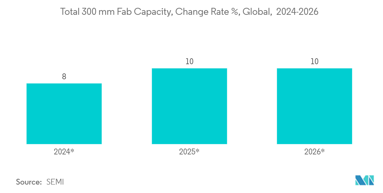
- The rate of global 300 mm fab capacity expansion is slowing down. However, the industry is still dedicated to increasing capacity to keep up with the firm and consistent semiconductor demand. For instance, in March 2024, India planned to produce equipment for semiconductor manufacturing, with Applied Materials taking the lead by establishing a validation center in Bengaluru. The country is also advancing in 300 mm wafer processing and is focusing on creating a supportive ecosystem while establishing an engineering center. These innovations are driving the growth of the market studied.
- In November 2023, Texas Instruments launched a new 300 mm semiconductor wafer fabrication plant called LFAB2 in Lehi, Utah. The construction of LFAB2 will be connected to the company's existing 300 mm wafer fab in the exact location. Once LFAB2 is finished, both of TI's Utah fabs will be capable of producing tens of millions of embedded and analog processing chips daily at maximum capacity. LFAB2 aims to operate solely on renewable electricity, and the implementation of advanced 300 mm equipment and processes in Lehi will help minimize waste, water, and energy usage.
- The shift to 300 mm wafer size is often associated with adopting advanced semiconductor manufacturing technologies and smaller process nodes (7 nm and 5 nm). These advanced node technologies require tighter process control and enhanced polishing to meet stringent performance and reliability requirements.
- Chemical mechanical polishing (CMP) pads are in high demand because they play a crucial role in achieving the nanoscale-level planarity required for advanced node fabrication.

Asia-Pacific to Hold Significant Market Share
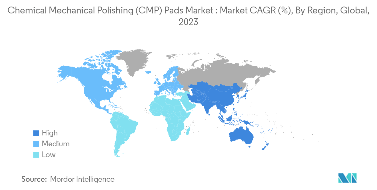
- Asia-Pacific is a global semiconductor manufacturing hub, with countries like China, Taiwan, South Korea, and Japan playing significant roles in semiconductor fabrication. The region's growth in semiconductor manufacturing drives the substantial demand for chemical mechanical polishing (CMP) pads used in wafer polishing processes.
- Asia-Pacific is at the forefront of technological advancements, including developing advanced packaging technologies, high-performance computing, and AI (artificial intelligence). These advancements require precise and efficient CMP processes, boosting the demand for CMP pads.
- The region continues to witness investments in new semiconductor fabrication facilities (fabs) and the expansion of existing ones. Increasing fab capacity and installing advanced manufacturing equipment contribute to the higher consumption of CMP pads. For instance, in March 2024, Tata Electronics Private Limited (TEPL) partnered with Taiwan's Powerchip Semiconductor Manufacturing Corp. (PSMC) to set up a semiconductor fab in Dholera, Gujarat. The investment for this project is INR 9,100 billion (USD 109.71 billion). PSMC currently operates six semiconductor foundries in Taiwan.
- The capacity of the new fabs will be 50,000 wafer starts per month. PSMC will focus on producing high-performance compute chips using 28 nm technology and power management chips for various industries such as electric vehicles, telecom, defense, automotive, consumer electronics, display, and power electronics.
- Asia-Pacific is home to a large and expanding consumer electronics market driven by rising disposable incomes, urbanization, and technological proliferation. The demand for smartphones, laptops, and electronic devices fuels the need for semiconductor components and CMP pads.
- Moreover, emerging economies in Asia-Pacific, such as India, Vietnam, and Indonesia, are witnessing increasing adoption of semiconductor technologies across various sectors. As these economies continue to industrialize and digitize, the demand for CMP pads for semiconductor manufacturing is expected to grow significantly.
- Ongoing infrastructure development projects, such as smart cities, 5G networks, and the IoT, drive demand for semiconductor chips and electronic components. The chemical mechanical polishing (CMP) pads play a significant role in enabling the production of advanced semiconductor devices required for these infrastructure projects.
- In addition, governments and industries in Asia-Pacific are investing in semiconductor R&D to foster innovation. Research initiatives aimed at developing next-generation materials, devices, and processes contribute to the demand for CMP pads.


