Market Size of Chemical Mechanical Polishing (CMP) Pad Industry

| Study Period | 2019 - 2029 |
| Market Size (2024) | USD 4 Billion |
| Market Size (2029) | USD 5.61 Billion |
| CAGR (2024 - 2029) | 7.90 % |
| Fastest Growing Market | North America |
| Largest Market | Asia Pacific |
| Market Concentration | Low |
Major Players
*Disclaimer: Major Players sorted in no particular order |
Chemical Mechanical Polishing (CMP) Pad Market Analysis
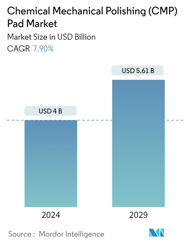
The Chemical Mechanical Polishing Pad Market size is estimated at USD 4 billion in 2024, and is expected to reach USD 5.61 billion by 2029, growing at a CAGR of 7.90% during the forecast period (2024-2029).
- Chemical mechanical polishing is a crucial step in the semiconductor wafer manufacturing process. During this process, the top surface of the wafer is polished to create a completely flat surface, which is essential for building more robust and durable semiconductor materials using a combination of chemical slurry and mechanical movements.
- The rising performance standards of electronic devices are leading to a need for smaller and more durable semiconductors and electronic devices. This, in turn, increases the requirement for advanced fabrication materials and techniques such as CMP. The growing demand for electronic products drives the electronic packaging industry, with customers expecting enhanced features in new electronic devices.
- The semiconductor industry is a significant consumer of chemical mechanical polishing pads, particularly for wafer polishing processes during semiconductor manufacturing. The increasing demand for semiconductors driven by applications such as automotive electronics, smartphones, IoT devices, and AI (artificial intelligence) technologies fuels the demand for chemical mechanical polishing pads. Moreover, the continuous technological advancements in semiconductor fabrication technologies, including the development of smaller feature sizes, drive the need for more precise and efficient CMP pads.
- The rising adoption of packaging technologies such as 3DE ICs, through-silicon vias(TSVs), and fan-out wafer-level packaging (FOWLP) necessitates advanced CMP polishing and surface preparation solutions. Chemical mechanical polishing (CMP) pads are crucial in achieving the required polishing, surface roughness, and defectivity levels of these advanced packaging processes.
- Despite the advancements in chemical mechanical polishing (CMP) pad materials and manufacturing processes, certain technological limitations persist. These limitations include achieving ultra-smooth surfaces, controlling sub-surface damage, minimizing edge effects, and addressing pad wear and slurry consumption issues. Overcoming these limitations may require further research and development efforts, thus hindering the market's growth. Moreover, CMP pad manufacturers may face risks associated with supply chain disruptions, impacting the ability to meet demand.
- Macroeconomic factors such as technological advancements, material science innovations, and process engineering developments are presenting challenges and opportunities for CMP pad manufacturers. Addressing technical difficulties related to CMP process control, defect reduction, material compatibility, and surface quality improvement drives R&D investments and product innovation in the CMP pads market. Conversely, breakthroughs in CMP pad materials, formulations, or manufacturing techniques can create competitive advantages and market opportunities for innovative suppliers.
Chemical Mechanical Polishing (CMP) Pad Industry Segmentation
CMP pads are integral to the semiconductor industry's CMP (chemical mechanical polishing or planarization) process, which is crucial for flattening and polishing silicon wafers. These pads, typically crafted from hard, porous polyurethane foam, feature intricate, high-aspect-ratio grooves. The study tracks the revenue generated from the sale of chemical mechanical polishing pads (CMP) offered by different market players for a diverse range of applications. The market trends are evaluated by analyzing the investments made in product innovation, diversification, and expansion. The study further analyses the aftereffects of COVID-19 and other macroeconomic factors on the market. The report's scope encompasses market sizing and forecasts for the various market segments.
The chemical mechanical polishing (CMP) pads market is segmented by wafer size (300 mm and 200 mm) and geography (North America, Europe, China, South Korea, Japan, Taiwan, and Rest of the World). The market sizes and forecasts are provided in terms of value (USD) for all the above segments.
| By Wafer Size | |
| 300 mm | |
| 200 mm | |
| Other Wafer Sizes |
| By Geography*** | |
| North America | |
| Europe | |
| China | |
| South Korea | |
| Japan | |
| Taiwan |
Chemical Mechanical Polishing (CMP) Pad Market Size Summary
The Chemical Mechanical Polishing (CMP) Pad Market is poised for significant growth, driven by the increasing demand for semiconductors and advanced electronic devices. CMP pads are essential in the semiconductor manufacturing process, particularly for wafer polishing, ensuring the surface is flat and ready for further processing. The push for smaller, more durable semiconductors to meet the rising performance standards of electronic devices is a key factor fueling this demand. The semiconductor industry, a major consumer of CMP pads, is experiencing growth due to applications in automotive electronics, smartphones, IoT devices, and AI technologies. The adoption of advanced packaging technologies further necessitates the use of CMP pads to achieve the required surface quality and defectivity levels. Despite technological advancements, challenges such as achieving ultra-smooth surfaces and minimizing pad wear persist, prompting ongoing research and development efforts.
The Asia-Pacific region plays a pivotal role in the CMP pad market, driven by its status as a global semiconductor manufacturing hub. Countries like China, Taiwan, South Korea, and Japan are at the forefront of semiconductor fabrication, with significant investments in new fabs and advanced manufacturing equipment. The region's expanding consumer electronics market and the rise of emerging economies contribute to the growing demand for CMP pads. Macroeconomic factors, including technological advancements and process engineering developments, present both challenges and opportunities for CMP pad manufacturers. The market is highly competitive, with major players like 3M Co, DuPont de Nemours Inc., and SK enpulse focusing on expanding their global presence through collaborations and product innovations. Environmental concerns have also led to initiatives like recycling CMP pads, highlighting the industry's commitment to sustainability.
Chemical Mechanical Polishing (CMP) Pad Market Size - Table of Contents
-
1. MARKET INSIGHTS
-
1.1 Market Overview
-
1.2 Industry Attractiveness - Porter's Five Forces Analysis
-
1.2.1 Threat of New Entrants
-
1.2.2 Bargaining Power of Buyers/Consumers
-
1.2.3 Bargaining Power of Suppliers
-
1.2.4 Threat of Substitute Products
-
1.2.5 Intensity of Competitive Rivalry
-
-
1.3 Technology Snapshot
-
1.4 Impact of COVID-19 Aftereffects and Other Macroeconomic Factors on the Market
-
-
2. MARKET SEGMENTATION
-
2.1 By Wafer Size
-
2.1.1 300 mm
-
2.1.2 200 mm
-
2.1.3 Other Wafer Sizes
-
-
2.2 By Geography***
-
2.2.1 North America
-
2.2.2 Europe
-
2.2.3 China
-
2.2.4 South Korea
-
2.2.5 Japan
-
2.2.6 Taiwan
-
-
Chemical Mechanical Polishing (CMP) Pad Market Size FAQs
How big is the Chemical Mechanical Polishing Pad Market?
The Chemical Mechanical Polishing Pad Market size is expected to reach USD 4 billion in 2024 and grow at a CAGR of 7.90% to reach USD 5.61 billion by 2029.
What is the current Chemical Mechanical Polishing Pad Market size?
In 2024, the Chemical Mechanical Polishing Pad Market size is expected to reach USD 4 billion.

