
Asia-Pacific Semiconductor Materials Market Size and Share
Market Overview
| Study Period | 2020 - 2031 |
|---|---|
| Forecast Data Period | 2026 - 2031 |
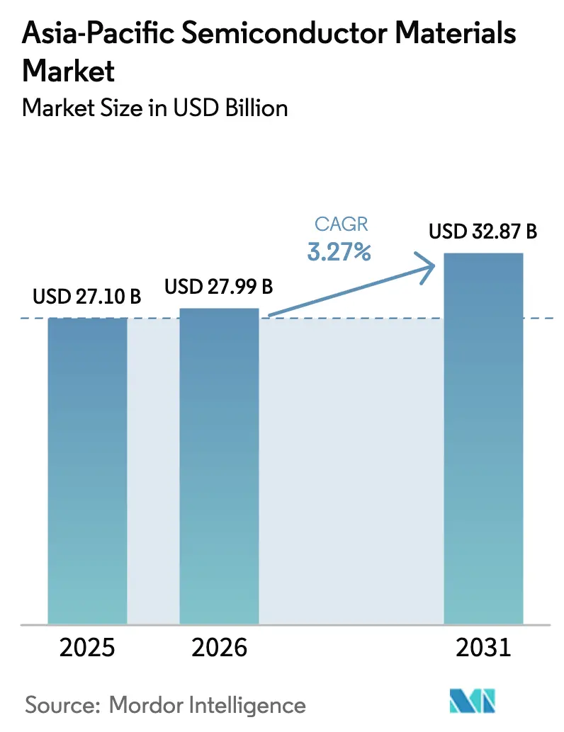
| Base Year Market Size (2025) | USD 27.10 Billion |
| Market Size (2026) | USD 27.99 Billion |
| Market Size (2031) | USD 32.87 Billion |
| Growth Rate (2026 - 2031) | 3.27 % |
| Market Concentration | Medium |
Major Players *Disclaimer: Major Players sorted in no particular order Image © Mordor Intelligence. Reuse requires attribution under CC BY 4.0. | |
Asia-Pacific Semiconductor Materials Market Analysis by Mordor Intelligence
The Asia-Pacific semiconductor materials market size is expected to grow from USD 27.10 billion in 2025 to USD 27.99 billion in 2026 and is forecast to reach USD 32.87 billion by 2031 at 3.27% CAGR over 2026-2031. Momentum comes from sovereign technology programs in China, Japan and Korea that prioritize local sourcing of specialty chemistries, while tighter design rules at sub-10 nm nodes are lifting per-wafer material content. Electric-vehicle electrification, mini/micro-LED investments and heterogeneous integration are enlarging demand for wide-bandgap substrates, advanced gases and novel under-fill compounds. At the same time, export-control compliance and water-scarcity mitigation are reshaping site-selection strategies, creating both risk and opportunity for regional suppliers. Competitive intensity is growing as new Chinese entrants target commodity segments, compelling incumbents to accelerate process innovation and expand local production footprints.
Key Report Takeaways
- By material, Silicon Wafers held the largest 37.74% share of the Asia-Pacific semiconductor materials market in 2025, while Silicon Carbide is forecast to grow fastest at 9.08% CAGR to 2031.
- By application, the Fabrication segment commanded 65.12% of the Asia-Pacific semiconductor materials market share in 2025; Advanced Packaging is expected to expand at a 6.84% CAGR to 2031.
- By end-user, Consumer Electronics accounted for 41.02% of the Asia-Pacific semiconductor materials market in 2025, but Automotive and Mobility is advancing at the highest 8.29% CAGR to 2031.
- By geography, Taiwan led with a 34.75% revenue share of the Asia-Pacific semiconductor materials market in 2025, whereas China is projected to post the quickest 3.92% CAGR through 2031.
Note: Market size and forecast figures in this report are generated using Mordor Intelligence’s proprietary estimation framework, updated with the latest available data and insights as of 2026.
Asia-Pacific Semiconductor Materials Market Trends and Insights
Drivers Impact Analysis*
| Driver | (~) % Impact on CAGR Forecast | Geographic Relevance | Impact Timeline |
|---|---|---|---|
| Government-backed chip sovereignty funds | +0.80% | China, Japan, Korea | Medium term (2-4 years) |
| Surge in SiC and GaN adoption for EV powertrains | +0.60% | China, Japan | Short term (≤ 2 years) |
| Mini/Micro-LED ramp-up elevating metal-organic demand | +0.40% | Korea, Taiwan | Medium term (2-4 years) |
| ASEAN re-shoring initiatives for backend materials | +0.30% | ASEAN | Long term (≥ 4 years) |
| Low-GWP fluorinated-gas mandates | +0.20% | Global | Short term (≤ 2 years) |
| Heterogeneous-integration materials for 2.5D/3D IC | +0.50% | Taiwan, Korea | Medium term (2-4 years) |
| Source: Mordor Intelligence | |||
Government-backed Chip Sovereignty Funds Accelerating New Material Fabs in China, Japan and Korea
Several Northeast-Asian governments are using dedicated chip funds to subsidize local material plants, shortening qualification cycles and lifting regional content in leading-edge fabs. In Korea, a USD 471 billion cluster in Gyeonggi Province targets 50% self-sufficiency in critical chemistries by 2030. [1] Japan is tying TSMC’s Kumamoto expansion to joint R&D programs with domestic photoresist and wafer suppliers, while China is channeling capital toward indigenous CMP slurries, electronic gases and fluorochemicals. These coordinated investments underpin steady demand even during cyclical downturns, giving the Asia-Pacific semiconductor materials market a structural growth floor.
Surge in SiC and GaN Adoption for EV Powertrains Across China and Japan
Electric-vehicle makers are shifting from silicon MOSFETs to SiC and GaN power devices to cut conduction losses and boost driving range. Chinese vertically integrated substrate pioneers have begun supplying 200 mm SiC wafers that meet automotive-grade defect density thresholds, helping local OEMs lock-in long-term contracts. Japanese material houses are parallel-tracking crystalline-quality improvements for GaN-on-Si epitaxy to serve on-board chargers. This transition is tilting material demand toward wide-bandgap substrates, epitaxial gases and high-temperature encapsulants, broadening the Asia-Pacific semiconductor materials market beyond its silicon core.
Mini/Micro-LED Ramp-up Driving Demand for High-Purity Metal-Organics in Korea and Taiwan
Commercial readiness of micro-LED displays with pixel densities above 500 PPI is pulling in unprecedented volumes of ultra-high-purity trimethyl-gallium, trimethyl-indium and precursors for quantum-dot color-conversion layers. Korean panel makers and Taiwanese OSATs are collaborating to co-optimize epitaxial growth and bump-bonding flows, raising the bar for impurity controls to parts-per-trillion. Suppliers capable of delivering such contamination thresholds at scale are capturing premium margins, reinforcing the value-add shift within the Asia-Pacific semiconductor materials market.
ASEAN Re-shoring Initiatives Creating Green-field Chemical Plants for Backend Materials
Malaysia, Vietnam and Thailand are stepping up incentives for local production of molding compounds, substrates and lead-frame alloys. Penang’s backend cluster alone tripled its factory space to 3.4 million ft² in 2025. Green-field plants in these markets shorten logistics loops for regional OSATs, diversify geo-political exposure and unlock lower-carbon utility footprints. As capacity migrates south, chemical vendors are adding localized mixing, purification and drum-recycling operations, widening the geographic spread of the Asia-Pacific semiconductor materials market.
Restraints Impact Analysis*
| Restraint | (~) % Impact on CAGR Forecast | Geographic Relevance | Impact Timeline |
|---|---|---|---|
| Volatile silicon and rare-metal prices | -0.40% | Global | Short term (≤ 2 years) |
| US/EU export controls delaying qualification in China | -0.60% | China | Medium term (2-4 years) |
| Ultrapure-water scarcity | -0.30% | Taiwan, Singapore | Long term (≥ 4 years) |
| Lengthy EHS permitting for chemical plants | -0.20% | Korea | Medium term (2-4 years) |
| Source: Mordor Intelligence | |||
Volatile Silicon and Rare-Metal Prices Squeezing Fab Margins
Spot silicon-wafers and crucible-grade quartz have exhibited double-digit price swings amid tight supply chains concentrated in a handful of mines. Parallel spikes in gallium and germanium prices, following export-license restrictions, are forcing fabs to re-negotiate long-term contracts and hedge commodity exposure. Because material outlays can represent 25-30% of wafer-fabrication cash costs, these fluctuations compress profitability and temper expansion plans, keeping the Asia-Pacific semiconductor materials market on a cautious capital-expenditure footing.
US/EU Export Controls Delaying Material Qualification in Mainland China
Expanded Foreign Direct Product rules issued in December 2024 now require special licenses for a wider set of photoresists, lithography gases and deposition precursors destined for advanced Chinese fabs. [2] As compliance audits lengthen, local foundries are forced to dual-source or initiate in-house development, stretching qualification timelines by 6-12 months. The lag slows node migrations and curbs near-term material volumes, subtracting 0.6 percentage points from the Asia-Pacific semiconductor materials market CAGR during the forecast window.
*Our forecasts treat driver/restraint impacts as directional, not additive. The impact forecasts reflect baseline growth, mix effects, and variable interactions.
Segment Analysis
By Material: Wide-Bandgap Semiconductors Drive Innovation
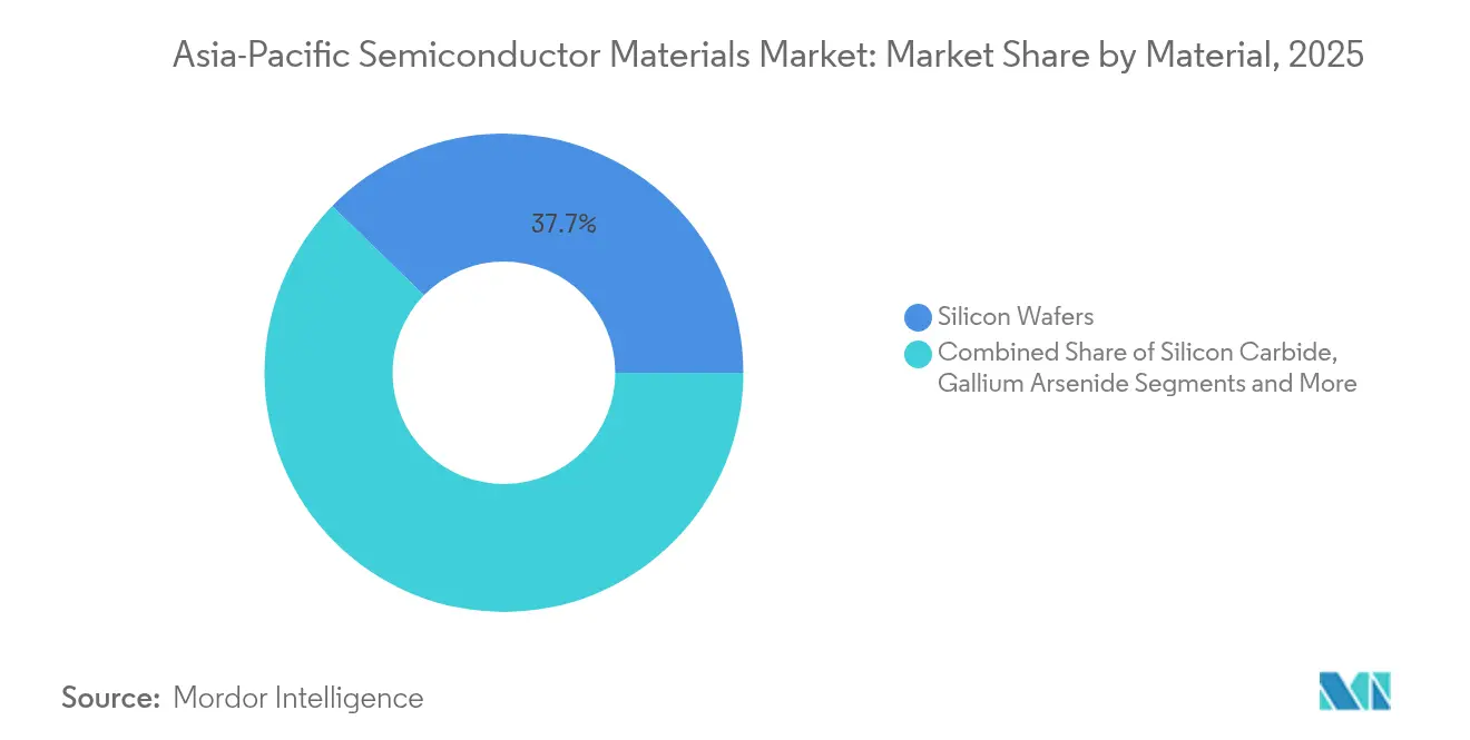
Silicon Wafers retained the largest 37.74% share of the Asia-Pacific semiconductor materials market in 2025, supported by capacity additions at 5 nm and 3 nm nodes. Yet Silicon Carbide is the clear growth engine, expanding at 9.08% CAGR as vehicle electrification and renewable grids demand high-voltage efficiency. This shift is enlarging the Asia-Pacific semiconductor materials market size for wide-bandgap substrates, gases and polishing slurries that meet stringent surface-defect criteria. GaN and GaAs materials are also gaining traction for 5G base-stations and RF front-ends, even though substrate costs remain a cap on volume adoption.
Process innovation is bringing 200 mm SiC wafers to pilot scale, with defect densities below 0.1 cm⁻² setting new automotive benchmarks. At the same time, the Korea Research Institute of Chemical Technology’s breakthrough in hydrofluoroether synthesis improves local supply security for advanced etch chemistries. As these technical milestones reduce unit costs and raise reliability, they reinforce a performance-over-price paradigm that re-shapes procurement decisions within the Asia-Pacific semiconductor materials market.

By Application: Advanced Packaging Reshapes Material Demands
Fabrication consumed 65.12% of total material revenues in 2025, anchored by lithography-heavy logic and memory expansions. Electronic specialty gases represent the fastest-growing fabrication sub-segment, climbing at 8.11% CAGR as patterning complexity increases. However, Advanced Packaging is the headline growth story, rising 6.84% annually as chiplet and 3D-stack architectures move into high-volume manufacturing. The Asia-Pacific semiconductor materials market size tied to organic and ceramic substrates is projected to reach USD 10.06 billion by 2031, with under-fill and dielectric films advancing in tandem.
TOPPAN’s coreless organic interposer allows fine-pitch interconnects below 10 µm, eliminating build-up layers and reducing package Z-height. Copper-to-copper hybrid bonding is simultaneously displacing traditional solder bumps, pushing demand for oxide-removal cleaners and low-temperature diffusion barriers. Together, these advances expand material-count per package and diversify the bill-of-materials, adding resilience to the Asia-Pacific semiconductor materials market.
By End-user: Automotive Transformation Accelerates
Consumer Electronics still represented 41.02% of the Asia-Pacific semiconductor materials market in 2025, but unit growth is plateauing. In contrast, Automotive and Mobility is escalating at 8.29% CAGR, propelled by battery-electric drivetrain volumes and the proliferation of advanced driver-assistance systems. A premium electric vehicle can now carry USD 1,600-1,900 worth of semiconductors, double that of an entry-level smartphone, creating a lucrative pull for AEC-Q101-qualified wafers, encapsulants and power modules. These dynamics are redistributing the Asia-Pacific semiconductor materials market share toward suppliers with automotive-grade certification capabilities.
Parallel tailwinds exist in data-center processors and high-performance computing accelerators, where packaging materials with superior thermal conductivity and low-loss dielectrics are mission-critical. Telecom infrastructure, industrial automation and medical electronics round out the demand profile, each segment adding specialized requirements that raise the overall technical ceiling-and barriers to entry-within the Asia-Pacific semiconductor materials market.
Geography Analysis
Taiwan captured 34.75% of the Asia-Pacific semiconductor materials market in 2025, thanks to its dense ecosystem linking logic foundries, memory fabs and advanced packaging houses. Close physical proximity between fabs and material suppliers reduces cycle time for slurry, resist and specialty-gas qualifications, reinforcing Taiwan’s leadership. Yet water-stress projections show semiconductor plants could raise local water demand 236% between 2021 and 2030, prompting accelerated adoption of closed-loop reclamation systems. Energy-price volatility adds further cost pressure, encouraging fabs to shift incremental capacity for mature nodes to alternate hubs.
China is the fastest-growing market, forecast at a 3.92% CAGR through 2031 as industrial-policy incentives, tax rebates and land grants underwrite domestic sourcing programs. While export-control headwinds persist, tier-1 Chinese foundries are qualifying indigenous slurries, photoresists and CMP pads for 28 nm nodes and below. Regional material parks in Anhui, Hubei and Guangdong bundle gas farms, chemical mixing and waste-treatment facilities, reducing inbound logistics costs by up to 15%. As localization takes hold, the Asia-Pacific semiconductor materials market gains a second gravitational center beyond Taiwan.
South Korea’s USD 471 billion mega-cluster will add new demand for lithography chemicals, ALD precursors and high-bandwidth-memory substrates, with SK Hynix alone budgeting USD 75 billion to 2028. Japan, already a top exporter of fluorinated gases and photo-initiators, is bolstering resilience by constructing its first domestic 300 mm wafer plant in over five decades. Meanwhile, ASEAN countries-led by Malaysia and Vietnam-are scaling backend assembly and selectively moving into front-end pilot lines. This geographic diversification diffuses single-country risk while enlarging the overall addressable base of the Asia-Pacific semiconductor materials market.
Value Chain Analysis
Upstream inputs for semiconductor materials in Asia-Pacific start with high-purity feedstocks and specialty intermediates, including electronic-grade silicon and compound-semiconductor precursors, as well as high-purity inorganic fillers used in packaging. These inputs move into purification, synthesis, and crystal-growth steps that are often tightly integrated by leading suppliers. For example, Shin-Etsu Chemical combines capabilities spanning silicon wafers and lithography-related materials, while Merck Electronics expands regional production of specialty gases and thin-film materials via its Kaohsiung, Taiwan investment (about EUR 500 million), targeting higher self-sufficiency for nearby fabs and OSATs.
Midstream manufacturing includes wafer substrates (silicon and emerging wide-bandgap options), process chemicals (wet etchants, solvents, and CMP slurries), electronic gases, photoresist systems, and packaging materials such as substrate cores, underfills, and encapsulants. Downstream demand concentrates in large-scale foundries, IDMs, memory makers, and OSATs across Taiwan, Korea, Japan, China, and ASEAN, where qualification cycles and contamination control shape long-term, specification-led supply relationships. The chain is increasingly influenced by co-development between materials and packaging ecosystems, including Dongwoo Fine-Chem (Sumitomo Chemical) supporting infrastructure for Korea-based initiatives and the region-wide push toward advanced packaging materials that add new steps and suppliers to the bill-of-materials.
Competitive Landscape
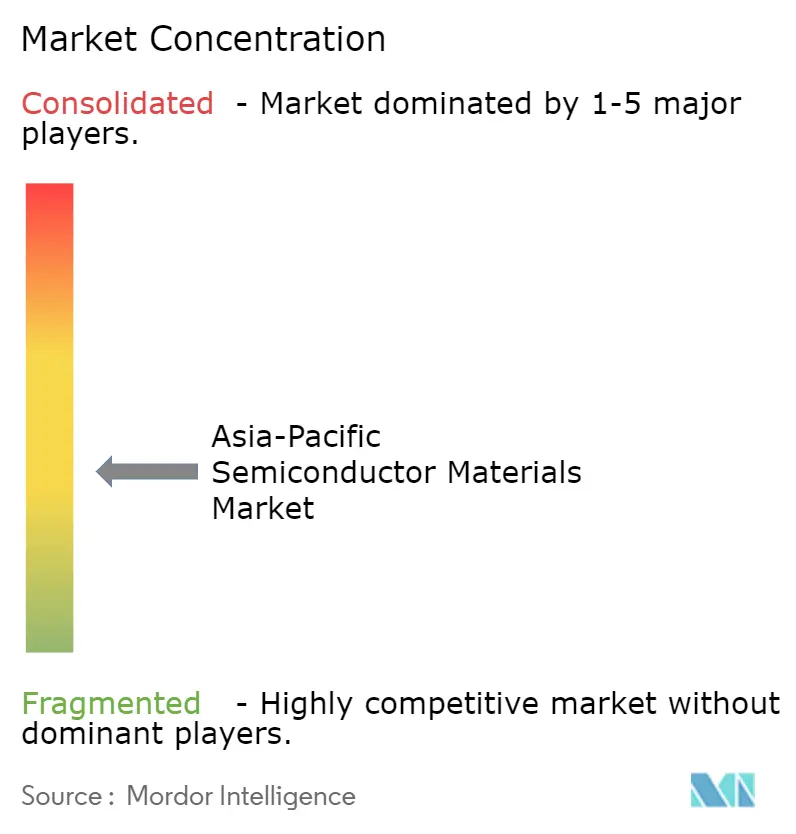
The Asia-Pacific semiconductor materials market shows moderate fragmentation. In value-added niches such as EUV photoresists, less than five suppliers meet stochastic-defect targets, whereas bulk chemicals face intense price competition from new Chinese producers. Incumbent Japanese and European firms are responding by deepening local manufacturing: Shin-Etsu is expanding wafer capacity in Japan after a 56-year hiatus, and BASF is constructing a semiconductor-grade sulfuric-acid plant to tighten control over upstream supply. [3]
Technology co-development is emerging as a key differentiator. The US-JOINT consortium, which includes 3M, is pooling resources to accelerate non-PFAS surface-modifier research, seeking drop-in replacements ahead of regulatory bans. In packaging, Applied Materials’ 9% stake in BE Semiconductor is aimed at hybrid-bonding line-integration, ensuring equipment-to-material process compatibility. Such alliances underscore a strategic pivot from scale-based competition toward ecosystem orchestration within the Asia-Pacific semiconductor materials market.
Chinese challengers are gaining traction in commodity segments such as sputter targets and wet chemicals by leveraging cost-advantaged energy tariffs and state-backed financing. Qualification barriers remain steep for safety-critical chemistries, yet once approved, domestic suppliers can rapidly scale, pressuring incumbents on margin. Taken together, these dynamics point toward a landscape where intellectual-property depth, regional manufacturing breadth and ESG compliance ultimately determine share capture in the Asia-Pacific semiconductor materials market.
Asia-Pacific Semiconductor Materials Industry Leaders
-
Shin-Etsu Chemical Co., Ltd.
-
Sumitomo Chemical Co., Ltd.
-
Merck KGaA (incl. Versum Materials)
-
Air Liquide S.A.
-
BASF SE
- *Disclaimer: Major Players sorted in no particular order
Market Opportunities and Future Outlook
Advanced packaging is creating distinct whitespace for Asia-Pacific material suppliers as glass-core and fine-line substrate roadmaps move beyond conventional organic cores. A concrete signal is the July 2026 joint venture agreement between Dongwoo Fine-Chem (Sumitomo Chemical) and Samsung Electro-Mechanics (GlaSSEM) to produce glass core substrates in Pyeongtaek, Korea (operations scheduled for the second half of 2027), which supports demand for substrate-grade glass, surface-treatment chemistries, metallization-related materials, and inspection-grade process consumables linked to higher-density interconnect schemes.
Localization programs and new capacity announcements also broaden the addressable base for photoresists, specialty gases, and upstream purification services, while increasing the premium on onshore qualification support near fabs. Shin-Etsu Chemical’s build-out of its fourth semiconductor lithography materials production base in Isesaki City, Gunma Prefecture, with initial investment completion scheduled for 2026, reinforces continued regional investment in lithography materials that are constrained by quality requirements and supply assurance. India’s Semicon 2.0 approval on July 15, 2026 (Rs 1,27,500 crore) adds policy-backed activity across design and manufacturing, creating entry points for suppliers that can offer local blending, purification, analytical services, and waste-handling capabilities aligned with fab EHS requirements and faster qualification cycles.
Recent Industry Developments
- July 2026: Sumitomo Chemical Co., Ltd. and Samsung Electro-Mechanics signed a joint venture to establish a company for glass core substrates in 2026. The move expands back-end materials capacity for advanced packaging and strengthens capability in glass core substrates. The collaboration signals a strategic push to secure regional supply chains for APAC customers.
- May 2026: Sumitomo Chemical Co., Ltd. announced the launch of the ELA series, a new high-purity fine spherical alumina product line for advanced semiconductor applications. The new material broadens the portfolio for critical device materials in APAC. The initiative supports higher performance packaging and device reliability across regional customers.
- May 2026: Merck KGaA (Merck Electronics) reported progress on a 500 million euro plant in Kaohsiung, Taiwan, with mass production scheduled for 2027. The development adds regional semiconductor materials capacity in Taiwan. It strengthens local supply chains and capacity for APAC customers.
Research Methodology Framework and Report Scope
Market Definition and Coverage
For this study, the market covers revenues earned from materials that are used to manufacture semiconductors across Asia-Pacific, from wafer making through front-end and back-end processing steps. The value is captured at the point where materials are sold into chipmaking and packaging supply chains in the region.
Scope exclusions: It excludes semiconductor manufacturing equipment and services, and it does not count finished semiconductor devices as materials revenue.
Segmentation Overview
- By Material
- Silicon Wafers
- Silicon Carbide (SiC)
- Gallium Arsenide (GaAs)
- Gallium Nitride (GaN)
- Silicon Germanium (SiGe)
- Indium Phosphide (InP)
- Copper Indium Gallium Selenide (CIGS)
- Molybdenum Disulfide (MoS?)
- Bismuth Telluride (Bi?Te?)
- Other Materials
- By Application
- Fabrication
- Process Chemicals
- Photomasks
- Electronic Gases
- Photoresist Ancillaries
- Sputtering Targets
- Silicon Wafers
- CMP Slurries and Pads
- Other Fabrication Materials
- Packaging
- Substrates
- Lead Frames
- Ceramic Packages
- Bonding Wire
- Encapsulation Resins
- Die-Attach Materials
- Other Packaging Materials
- Fabrication
- By End-user Industry
- Consumer Electronics
- Telecommunication and 5G Infrastructure
- Industrial and Manufacturing Automation
- Automotive and Mobility (EV, ADAS)
- Energy and Utility (Solar, Power Conversion)
- Data Centers and HPC
- Healthcare Devices
- Others
- By Geography
- Taiwan
- South Korea
- China
- Japan
- Rest of Asia-Pacific
Data Sources, Market Sizing, and Validation
Desk Research
Desk research was used to set the market boundary and to build the first demand picture for materials tied to semiconductor output in Asia-Pacific. We referenced public sources such as SEMI releases and materials commentary, World Semiconductor Trade Statistics (WSTS) updates, national statistical agencies in key chipmaking countries, customs trade statistics for chemicals and electronic materials, and patent databases to understand where process intensity is rising.
On top of this, we reviewed company filings, investor presentations, earnings call transcripts, and trusted industry press to map capacity additions, node transitions, and packaging ramp-ups that affect material consumption per wafer. A paid subscription for company financials and news helped verify timelines and cross-check revenue direction at the supplier level. This list is illustrative, and many other public and paid sources were also used for data collection, validation, and clarification during the work.
Primary Interviews and Surveys
Primary inputs came from interviews and surveys with materials suppliers, distributors, and process specialists, along with buyers from fabs and OSATs. This channel of input helped us test the desk-research assumptions on volume direction, pricing movement, and how material mix changes between mature nodes and advanced nodes show up in day-to-day purchasing.
Coverage was spread across major Asia-Pacific manufacturing hubs, and the questionnaire specifically targeted near-term shifts in mix, the timing from capacity announcements to material pull-through, and areas where suppliers saw demand firm up or soften.
Distribution of primary research fieldwork respondents
| Company type | Respondent position |
|---|---|
| Top tier: 25% | CXOs: 19% |
| Mid tier: 56% | Functional/Unit leaders: 27% |
| Smaller Players: 19% | Managers: 54% |
Market-Sizing & Forecasting
Market sizing started with a top-down build where semiconductor production indicators and trade-linked demand pools were used to reconstruct likely materials consumption in Asia-Pacific, and then value was derived by applying realistic pricing for major material groups. To keep the totals practical, the model was checked with selective bottom-up approximations, such as sampled supplier revenue splits by region, channel feedback on shipment direction, and ASP-times-volume sense checks for high-value materials.
Key inputs used in the model include regional wafer starts and utilization signals, announced fab and packaging capacity additions, node mix shifts that change material intensity, and pricing movement for high-purity chemicals and specialty wafers. When interview feedback indicated a gap, assumptions were adjusted using clear rules, such as timing delays between capacity announcement and material pull-through, and a conservative range for ASP pass-through during tight supply periods. For forecasting, scenario analysis was used around capacity ramp speed and pricing normalization, and the final trajectory was chosen based on the most common expert view across the respondent set.
Data Validation & Update Cycle
Outputs were validated through multiple checks, including comparing implied materials spend per wafer against historical ranges and reviewing whether growth matches fab utilization and packaging throughput signals. Outliers were flagged and reviewed by another analyst before sign-off, and follow-up outreach was triggered when interview feedback contradicted the model by more than a reasonable variance.
Reports are refreshed annually, with interim updates when material events occur, such as major capacity delays, policy changes that affect trade, or sharp pricing swings in key inputs. Before delivery, a final pass is completed so the latest public releases and company updates are reflected in the numbers and assumptions.
Mordor Intelligence's Asia Pacific Semiconductor Materials Market Size Versus Other Published Estimates
Published market values for Asia-Pacific semiconductor materials can differ even when the topic label sounds the same, because firms set different borders for what counts as a materials sale and how they treat regional splits. Differences also come from the timing of currency conversion, how pricing is progressed year to year, and how quickly estimates are updated when utilization and mix shift.
A refresh-led gap shows up when quarterly signals on wafer starts, packaging ramps, and short-cycle pricing are not folded into the model until much later, which can leave a prior-year snapshot being carried forward. By updating FX timing and ASP steps around key material groups and re-checking them against utilization and supplier commentary, Mordor Intelligence keeps the 2026 value tied to a current demand picture rather than a lagged average.
Benchmark comparison
| Source | Market Size | Gaps in Research Methodology |
|---|---|---|
| Mordor Intelligence | USD 27.99 B (2026) | |
| Industry Association A | USD 51.06 B (2024) | Uses a regional reporting structure that lists Taiwan, China, South Korea, and Japan separately, and many users back into an APAC total by partial addition, which can miss or double-count other Asia-Pacific countries depending on the mapping used. |
| Trade Journal B | USD 44.09 B (2024) | Often aggregates only the largest Asia manufacturing economies and applies a single-year USD conversion without adjusting for mix changes between advanced and mature nodes, which can understate the impact of higher material intensity per wafer. |
The table shows that most of the spread comes from how the region is assembled and whether the estimate is a true Asia-Pacific total or a partial roll-up of a few reported buckets. When scope rules, FX timing, and ASP progression are documented and re-tested against utilization and capacity ramp signals, the result becomes easier to trace and to replicate from one update to the next.
Key Questions Answered in the Report
What is the current value of the Asia-Pacific semiconductor materials market?
The market stands at USD 27.99 billion in 2026 and is projected to reach USD 32.87 billion by 2031 at a 3.27% CAGR.
Which country holds the largest share of the Asia-Pacific semiconductor materials market?
Taiwan leads with a 34.75% revenue share in 2025, driven by its concentration of advanced logic and packaging facilities.
Which material category is growing the fastest?
Silicon Carbide is expanding at 9.08% CAGR between 2026 and 2031 owing to electric-vehicle power-electronics adoption.
Why is advanced packaging important for material suppliers?
Chiplet and 3D-stack designs boost demand for innovative under-fill, substrate and bonding materials, lifting Advanced Packaging revenues at a 6.84% CAGR.
How are export controls affecting the Asia-Pacific semiconductor materials market?
New US/EU rules lengthen material qualification for Chinese fabs by up to 12 months, subtracting 0.6 percentage points from the regional CAGR.
What environmental issues influence investment decisions?
Water scarcity in Taiwan and Singapore, along with forthcoming PFAS regulations, are prompting fabs and suppliers to adopt reclamation systems and develop non-fluorinated chemistries.