
Asia-Pacific Semiconductor Device Market Size and Share
Market Overview
| Study Period | 2020 - 2031 |
|---|---|
| Forecast Data Period | 2026 - 2031 |
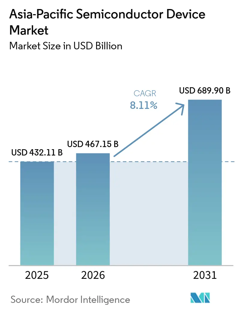
| Base Year Market Size (2025) | USD 432.11 Billion |
| Market Size (2026) | USD 467.15 Billion |
| Market Size (2031) | USD 689.90 Billion |
| Growth Rate (2026 - 2031) | 8.11 % |
| Market Concentration | Medium |
Major Players *Disclaimer: Major Players sorted in no particular order Image © Mordor Intelligence. Reuse requires attribution under CC BY 4.0. | |
Asia-Pacific Semiconductor Device Market Analysis by Mordor Intelligence
Asia-Pacific semiconductor device market size in 2026 is estimated at USD 467.15 billion, growing from 2025 value of USD 432.11 billion with 2031 projections showing USD 689.9 billion, growing at 8.11% CAGR over 2026-2031. Robust demand for advanced logic, memory, and power devices, combined with expanding regional capacity, underpins this trajectory. Momentum is reinforced by government subsidies for sub-7 nm manufacturing, the rollout of 5G and emerging 6G networks, and accelerating electrification across transportation and renewable energy systems. Tight node migration schedules at leading foundries and sustained capital spending by memory producers keep utilization rates high even as macroeconomic volatility persists. Intensifying competition for skilled talent and utilities places additional emphasis on productivity improvements, advanced packaging, and sustainability-aligned process upgrades. Nonetheless, the Asia-Pacific semiconductor device market remains the principal hub for global wafer output, ecosystem depth, and technology leadership.
Key Report Takeaways
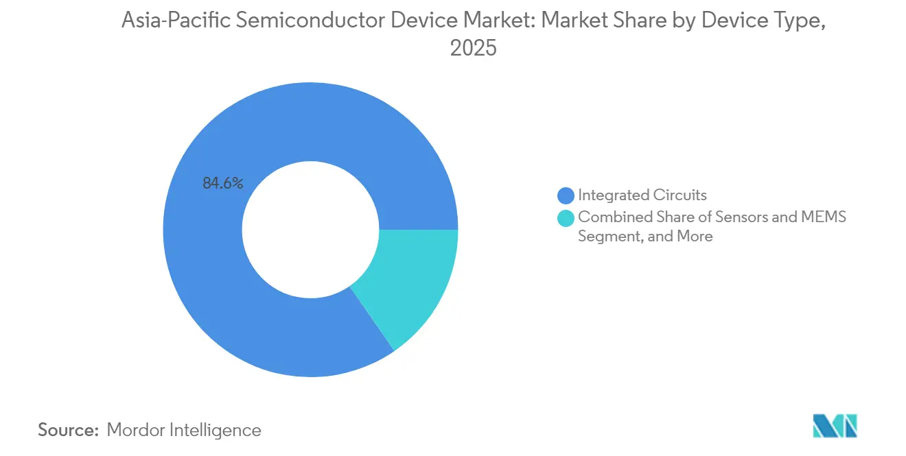
- By device type, integrated circuits captured 84.62% of the Asia-Pacific semiconductor device market share in 2025, while sensors and MEMS are projected to expand at a 9.54% CAGR through 2031.
- By business model, the IDM segment held 67.05% of the Asia-Pacific semiconductor device market share in 2025; fabless design vendors record the highest projected CAGR at 8.76% during 2026-2031.
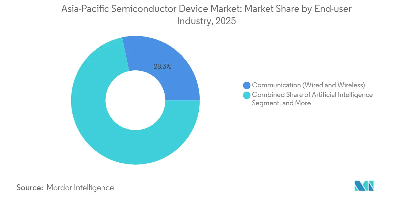
- By end-user industry, communication applications accounted for a 28.31% of the Asia-Pacific semiconductor device market share in 2025, whereas artificial intelligence workloads are advancing at a 9.72% CAGR to 2031.
- By country, China led with 51.62% of the Asia-Pacific semiconductor device market share in 2025, yet India is forecast to grow fastest at 9.29% CAGR through 2031.
Note: Market size and forecast figures in this report are generated using Mordor Intelligence’s proprietary estimation framework, updated with the latest available data and insights as of 2026.
Global valuation is built by aggregating outputs from multiple regions, with Asia forming one of the important contributors. Mordor Intelligence's global semiconductor device market size report represents that cumulative total.
Asia-Pacific Semiconductor Device Market Trends and Insights
Drivers Impact Analysis*
| Driver | (~) % Impact on CAGR Forecast | Geographic Relevance | Impact Timeline |
|---|---|---|---|
| AI-centric compute demand surge | +2.8% | Taiwan, South Korea, China | Medium term (2-4 years) |
| Electrification and ADAS in vehicles | +1.9% | China, Japan, South Korea | Long term (≥ 4 years) |
| 5G/6G network roll-outs | +1.5% | China, South Korea, Japan, ASEAN | Medium term (2-4 years) |
| Regional subsidies for sub-7 nm fabs | +1.2% | Japan, South Korea, Taiwan, India | Long term (≥ 4 years) |
| PV/ESS boom boosting wide-band-gap power devices | +0.8% | China, Japan, South Korea | Medium term (2-4 years) |
| In-house silicon by hyperscale cloud providers | +0.6% | Global demand, Asia-Pacific production | Short term (≤ 2 years) |
| Source: Mordor Intelligence | |||
AI-centric compute demand surge
AI accelerators for generative and edge inference workloads continue to strain foundry capacity, with TSMC’s advanced nodes (7 nm and finer) representing 74% of the company's wafer revenue in 2024. SK hynix lifted quarterly operating profit to a record KRW 8.08 trillion on high-bandwidth memory (HBM) sales that quadrupled year over year. Demand for high-bandwidth memory is one driver of the Asia Pacific semiconductor memory market.[1] Samsung has earmarked KRW 47.5 trillion for memory expansion focused on HBM3E and 3-nm gate-all-around logic to meet AI server demand. Foundries are scaling 2.5-D and 3-D chiplet packaging lines, yet substrate constraints keep lead times elevated into 2026. Continuous optimization of neural network architectures, including sparse computation and in-memory processing, is expected to reduce die size per TOPS but raise total wafer starts as AI permeates PCs, smartphones, and industrial edge nodes.
Electrification and ADAS in vehicles
China established domestic standards for more than 30 critical automotive semiconductors by 2025 to curb import dependence, accelerating local SiC and MCU sourcing. Regional EV adoption fuels incremental silicon content, with Southeast Asian vehicle output shifting toward battery electric platforms that require up to 2.5 times more power devices per unit than internal-combustion equivalents. Samsung Electro-Mechanics forecasts 11% annual growth in automotive MLCC shipments and plans production of the first LiDAR-grade capacitors in 2025. STMicroelectronics retains 32.6% share of the global SiC power market and is adding capacity in Catania and Wuxi to support double-digit CAGR through 2030. Mandatory functional-safety standards such as ISO 26262 continue to drive demand for high-reliability, automotive-grade ICs across propulsion, sensing, and zonal control domains.
5G/6G network roll-outs
China closed 2023 with 90% 5G penetration, operating 1.7 million base stations, and is targeting 1.6 billion 5G subscribers by 2030. South Korea pioneered 5G standalone deployments and now leads early-phase 6G trials leveraging 3GPP Release 20 features. India’s spectrum auctions and infrastructure build-out support a USD 1 trillion digital economy vision by 2025, with tower and small-cell installations rising 5.1% year on year to 5.79 million sites across Asia-Pacific. Higher-band carrier aggregation, integrated sensing, and sub-THz links for 6G will increase RF-front-end complexity, raising die demand for gallium nitrogen-on-silicon switches and power amplifiers. Network densification underpins ongoing investment in fronthaul optical transceivers, base-band ASICs, and timing ICs produced primarily in Taiwan and Japan.
Regional subsidies for sub-7 nm fabs
Japan awarded an additional JPY 590 billion (USD 3.9 billion) to Rapidus, lifting public funding to JPY 920 billion for a 2 nm process ramp in Hokkaido. South Korea’s KRW 471 trillion semiconductor super-cluster plan envisions 16 new fabs and 7.7 million wafer starts per month by 2030. India’s Semiconductor Mission offers 50% capital support to greenfield fabs, supplemented by state incentives that lift overall subsidies to 75% of the eligible outlay. Taiwan maintains a preferential tax rate of 5% on reinvested profits for semiconductor R&D and equipment purchases, sustaining domestic foundry dominance. Such measures strengthen regional competitiveness yet risk oversupply if global demand downshifts in late-decade cycles.
Restraints Impact Analysis*
| Restraint | (~) % Impact on CAGR Forecast | Geographic Relevance | Impact Timeline |
|---|---|---|---|
| Export controls on advanced lithography and EDA | −1.8% | China, Taiwan, South Korea | Medium term (2-4 years) |
| Acute design-engineering talent shortage | −1.4% | Taiwan, Japan, South Korea, India | Long term (≥ 4 years) |
| Water-energy sustainability constraints on fabs | −0.9% | Taiwan, Japan, China | Medium term (2-4 years) |
| Memory down-cycles throttling CAPEX | −0.7% | South Korea, Taiwan, China | Short term (≤ 2 years) |
| Source: Mordor Intelligence | |||
Export controls on advanced lithography and EDA
Successive U.S. Bureau of Industry and Security rulings since 2022 restrict EUV scanners, direct-write e-beam tools, and advanced EDA software sales to Chinese fabs. The Netherlands and Japan aligned policies in 2024, extending licensing to deep-UV multipatterning and PECVD equipment.[2] China retaliated by excluding certain U.S. processors from government procurement and boosting domestic fab approvals worth USD 46 billion. Multinational IDMs must navigate divergent compliance frameworks, elevating legal and logistical expenses. Yet, provincial subsidies and tier-two EDA vendors support ongoing 28 nm and mature-node expansions, tempering the near-term drag on the broader Asia-Pacific semiconductor device market.
Acute design-engineering talent shortage
Asia-Pacific requires up to 1 million additional skilled workers by 2030 as wafer volumes climb and design cycles shorten. Taiwan alone projects a 34,000-person gap, prompting universities to double graduate program intake and industry to fund fast-track certificate courses. India courts overseas engineers with tax holidays and expedited visas, whereas Japan eases language requirements for foreign PhDs. Rising salary demands, reaching 20% premiums for FinFET design roles, and squeezed margins, especially at smaller fabless firms. Companies respond by automating verification, adopting AI-assisted layout tools, and expanding remote design centers in Vietnam and Malaysia.
*Our forecasts treat driver/restraint impacts as directional, not additive. The impact forecasts reflect baseline growth, mix effects, and variable interactions.
Segment Analysis
By Device Type: Continued IC Dominance with Sensor Upside
Integrated circuits generated 84.62% of the Asia-Pacific semiconductor device market revenue in 2025 and are projected to retain leadership through 2031 as leading-edge logic, HBM, and LPDDR6 volumes scale. Node transitions to 3 nm and the planned 2 nm pilot line at Rapidus reinforce the high value density of logic die produced in the region. Memory’s cyclical rebound, anchored by AI server demand, lifts blended wafer ASPs, while automotive-grade MCUs call for embedded MRAM features on 28 nm processes in Japan and China.
The sensors and MEMS category is forecast to outpace the broader Asia-Pacific semiconductor device market at a 9.54% CAGR on rising automotive radar, lidar, and environmental sensing adoption in smart factories. The Asia-Pacific semiconductor device market size for MEMS motion sensors used in AR/VR headsets could exceed USD 4.32 billion by 2031. Optical and discrete power devices register mid-single-digit growth, buoyed by LED micro-display demand and SiC powertrain rollouts.

By Business Model: IDM Scale Meets Fabless Agility
IDMs held 67.05% of the Asia-Pacific semiconductor device market share in 2025, benefiting from capital depth, tight process control, and co-optimization of design with manufacturing. Samsung’s dual focus on memory and foundry amplifies economies of scope, while SK Hynix leverages vertical integration to dominate HBM supply. Automotive customers favor IDMs for longevity guarantees of up to 15 years.
Fabless firms, however, are growing faster at 8.76% CAGR owing to specialization in AI inference, custom network silicon, and RF front-end designs. MediaTek’s Dimensity series, RISC-V server SOCs from Chinese start-ups, and India’s new edge-AI MCU players exemplify this dynamism. Supply-chain resilience remains a concern as leading-edge capacity tightens, prompting multi-foundry tape-out strategies and collaborative design-technology-co-optimization (DTCO) programs with TSMC and UMC.
By End-user Industry: Communication Scale Versus AI Velocity
Communication infrastructure absorbed 28.31% of the Asia-Pacific semiconductor device market revenue in 2025, led by China Mobile’s 1.7 million 5G base stations and Japan’s first 5G-Advanced demonstrations. Massive MIMO radios and fronthaul optical modules depend on high-performance FPGAs and network processors built on 5 nm platforms.
Artificial intelligence workloads represent the fastest-growing application, advancing at a 9.72% CAGR as hyperscale, automotive, and industrial inference proliferate. Asia-Pacific semiconductor device market size for AI data-center silicon is projected to exceed USD 86.37 billion by 2031, supported by multi-layer HBM stacks exceeding 12 GB per package. Automotive electrification, industrial automation, and consumer electronics with on-device AI sustain diversified demand profiles across the region.
Geography Analysis
China commanded 51.62% of the Asia-Pacific semiconductor device market revenue in 2025, shipping 245.99 billion units despite export controls, and expanding capacity to 10.1 million wafers per month in 2025. Government backing, deep supply chains, and endemic electronics consumption underpin expansion across logic, memory, and discrete sectors. China’s unrivaled domestic scale sustains investment across mature and advanced nodes, even as export restrictions complicate equipment procurement. Local champions SMIC and YMTC adapt by deepening 28 nm capacity and innovating 3D NAND architectures. Taiwan’s “Silicon Shield” status is reinforced by TSMC’s 68.8% global foundry share and the company’s ongoing 1.4 nm pilot line in Taichung slated for 2028 volume.
India, with a 9.29% CAGR, emerges as the region’s growth engine. The USD 11 billion Tata-Powerchip fab and Micron’s USD 2.7 billion ATMP in Gujarat anchor the nascent ecosystem, while the Production-Linked Incentive scheme offsets up to 50% capex. South Korea doubles down on memory leadership through the Yongin mega-cluster, targeting first wafer starts in 2027 and integrating AI-driven fab automation for yield uplift. Japan leverages materials expertise and state subsidies to re-enter logic leadership with Rapidus’s 2 nm effort and a TSMC consortium fab in Kumamoto. India’s ambition to capture USD 100 billion in semiconductor output by 2030 hinges on streamlined environmental clearances and a deepening local design base.
Southeast Asian nations, notably Singapore and Malaysia, expand backend and specialty-analog clusters. Singapore’s 300 mm NXP-VIS joint venture targets 55,000 wafers per month by 2029, strengthening the city-state’s role as an advanced mixed-signal hub. Regional free-trade accords and favorable tax regimes continue to attract outsourced assembly and test service (OSAT) investments.
Coverage of the semiconductor device market by Mordor Intelligence spans a wide geographic footprint, with regional analysis available for Europe, alongside detailed country-level intelligence for South Korea, China, and Japan, each shaped by local operating conditions.
Regulatory Landscape
Regulatory influence on Asia-Pacific semiconductor devices is increasingly shaped by security and industrial-policy levers that affect qualification, market access, and equipment flows. In China, the Cyberspace Administration of China (CAC) expanded its Secure and Controllable certification scope in May 2026 to include automotive semiconductors, data center processors, and wireless communication chips, effectively gating many government and state-owned enterprise supply opportunities to certified vendors and architectures. Across the region, export-control alignment since 2024 on advanced lithography and certain process equipment continues to steer some Chinese capacity additions toward mature nodes, while raising compliance overhead for multinational IDMs and fabless-to-foundry supply chains.
At the same time, national programs are designed to pull more of the value chain onshore. India advanced its Semicon 2.0 program with a INR 1.27 trillion allocation supporting fabs and OSAT, complementing the existing incentive stack referenced in the market context. Vietnam updated its investment framework by allowing import of used semiconductor machinery up to 20 years old under Circular No. 30/2025, reducing capex barriers for backend and specialty lines, and it is pairing industrial policy with workforce targets under Resolution 57 and related decisions. Logistics and trade facilitation are also becoming operational-policy priorities for electronics exporters, illustrated by July 2026 coordination steps between SEIPI, the Bureau of Customs, and PEZA in the Philippines to expedite production-critical shipments amid airport warehouse congestion.
Value Chain Analysis
The Asia-Pacific semiconductor device value chain spans upstream materials and equipment, wafer manufacturing, advanced packaging and test, and downstream integration into communications, computing, automotive, and industrial systems. Wafer fabrication leadership remains concentrated in Taiwan, South Korea, Japan, and China (logic, memory, and power), while Southeast Asia plays a critical role in assembly, test, and selected specialty manufacturing. The region is also moving more capability into advanced packaging (2.5D/3D integration and chiplets) as AI and high-bandwidth memory raise substrate and packaging complexity, and as lead times and yield learning become key differentiators.
Recent events show the chain is sensitive to logistics continuity and to bottlenecks in critical inputs. The Philippines electronics ecosystem highlighted exposure to just-in-time imported materials when warehouse congestion at Ninoy Aquino International Airport required July 2026 coordination among industry (SEIPI) and agencies (Bureau of Customs, PEZA) to speed release of production-critical shipments. On the supply side, trade association SEMI has pointed to government efforts to address shortages of critical materials such as bromine and helium, reinforcing the importance of multi-sourcing and inventory strategies for fabs and OSATs. Capacity and capability additions are also being phased over multi-year horizons, with SK hynix scheduling construction of its M17 fab to begin in 2027 and targeting operations in the first half of 2029, while parallel investments in packaging support the device mix shift toward HBM-centric and AI-driven products.
Competitive Landscape
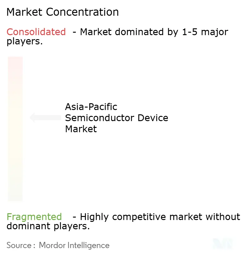
The Asia-Pacific semiconductor device market exhibits moderate concentration: the top five players command roughly 55-60% combined revenue, led by TSMC, Samsung, SK hynix, Micron, and SMIC. TSMC’s USD 165 billion global expansion includes three U.S. fabs and additional advanced packaging, safeguarding access for fabless customers while easing geopolitical supply-chain tensions.[4] Samsung balances foundry share gains against memory profitability by accelerating gate-all-around adoption at 3 nm. SK hynix strengthens its AI memory moat via 12-high HBM3E volumes shipped to Nvidia.
Rising challengers include Rapidus, backed by JPY 920 billion in subsidies, and India’s Tata Electronics. Chinese IDMs, buoyed by domestic demand, focus on specific niches like power discretes and NOR Flash. Strategic moves emphasize vertical integration, sustainability commitments, and co-development agreements: Denso-Rohm aligns on automotive SiC, Tenstorrent partners with Japan’s LSTC on 2 nm RISC-V accelerators, and 3M joins the US-JOINT materials consortium to expedite packaging innovation.
Supply-side risks remain concentrated in advanced lithography, specialty gases, and ABF substrates; firms mitigate exposure through multi-sourcing and long-term offtake contracts. Sustainability differentiation grows as TSMC, Samsung, and UMC pledge renewable energy targets exceeding 60% by 2030, aligning with customer ESG scorecard requirements.
Asia-Pacific Semiconductor Device Industry Leaders
-
Taiwan Semiconductor Manufacturing Company Limited (TSMC)
-
Samsung Electronics Co., Ltd.
-
SK hynix Inc.
-
Semiconductor Manufacturing International Corporation
-
United Microelectronics Corporation
- *Disclaimer: Major Players sorted in no particular order
Market Opportunities and Future Outlook
Whitespace in Asia-Pacific sits at the intersection of AI-driven compute, advanced packaging, and high-speed interconnect, where incremental value migrates from wafer-only scaling to heterogeneous integration. Government-backed and company-led plans in South Korea, including announced investments by Samsung and SK hynix in HBM fabs and packaging facilities, reinforce a regional push to expand both memory output and packaging throughput. This directly addresses substrate, packaging, and test constraints that have persisted alongside AI accelerator ramp cycles. The environment also supports opportunities for OSAT expansion, advanced packaging materials and tooling, and design-technology co-optimization programs that shorten time-to-yield for complex multi-die packages.
A second opportunity set comes from building new manufacturing and backend hubs to diversify supply chains and localize parts of the value chain. India moved beyond policy intent with Semicon 2.0 (INR 1.27 trillion allocation) spanning fabs and OSAT, and this broader support base creates room for local ecosystem formation across assembly/test services, specialty analog and power devices for electrification, and supplier localization for chemicals, gases, and components. Vietnam is pairing workforce targets (50,000 personnel training programs) with explicit goals for advanced testing and packaging plants by 2030, and it is strengthening linkages with Singapore-focused semiconductor associations and parks to deepen R&D and IC design collaboration. These programs, together with the region’s high share of global wafer output and continued demand from communications infrastructure and automotive electrification, keep the addressable pipeline broad across devices, nodes, and business models.
Recent Industry Developments
- July 2026: TSMC announced an additional USD 100 billion investment to build four more advanced wafer fabrication facilities in Arizona, taking its total U.S. commitment to USD 265 billion. The scale of the buildout supports tighter supply assurance for advanced-node customers and complements Asia-Pacific production by broadening geographic redundancy for critical logic and packaging supply.
- July 2025: TSMC began construction on four 1.4 nm plants in Central Taiwan Science Park, with a first-phase plan referenced at 50,000 wafers per month. The move reinforces Taiwan’s role as the advanced-logic anchor in the regional device ecosystem and increases downstream pull for advanced packaging, substrates, and specialty materials.
- February 2024: Japan awarded additional subsidies to Rapidus, lifting public funding to JPY 920 billion for its 2 nm process ramp in Hokkaido. The funding package strengthens Japan’s re-entry into leading-edge logic manufacturing and expands regional options for advanced-node collaboration and supply diversification.
Research Methodology Framework and Report Scope
Market Definition and Coverage
This market covers revenues generated from semiconductor devices sold into Asia-Pacific, counted at the point of device shipment to electronics manufacturing customers. The sizing reflects device categories used across major end markets in the region, and the figures are expressed in USD to keep cross-country comparability.
Scope exclusions: We exclude downstream electronic finished products and services revenue (for example, foundry services billed as processing and contract manufacturing value) that fall outside device sales.
Segmentation Overview
- By Device Type
- Discrete Semiconductors
- Diodes
- Transistors
- Power Transistors
- Rectifier and Thyristor
- Other Device Type
- Optoelectronics
- Light-Emitting Diodes (LEDs)
- Laser Diodes
- Image Sensors
- Optocouplers
- Other Optoelectronics
- Sensors and MEMS
- Pressure
- Magnetic Field
- Actuators
- Acceleration and Yaw Rate
- Temperature and Other Sensors and MEMS
- Integrated Circuits
- By IC Type
- Analog
- Micro
- Microprocessors (MPU)
- Microcontrollers (MCU)
- Digital Signal Processors
- Logic
- Memory
- By Technology Node
- less than 3 nm
- 3 nm
- 5 nm
- 7 nm
- 16 nm
- 28 nm
- Above 28 nm
- By IC Type
- Discrete Semiconductors
- By Business Model
- IDM
- Design/Fabless Vendor
- By End-user Industry
- Automotive
- Communication (Wired and Wireless)
- Consumer
- Industrial
- Computing/Data Storage
- Data Centre
- Artificial Intelligence
- Government (Aerospace and Defence)
- Other End-user Industry
- By Country
- China
- Japan
- South Korea
- Taiwan
- India
- Singapore
- Malaysia
- Australia
- Indonesia
- Rest of Asia-Pacific
Data Sources, Market Sizing, and Validation
Desk Research
Desk work starts by building a measurable demand pool for semiconductor devices in Asia-Pacific, then mapping it to regional production and trade signals. We lean on public time series and official publications to pin down cycle turns, product mix shifts, and major policy moves that can change shipment patterns.
Common references include World Semiconductor Trade Statistics releases (often republished through industry bodies), national statistics agencies for industrial output and external trade, customs and tariff-line trade datasets, central bank FX reference rates, and patent databases used to sanity-check activity in key device families. We also use company filings, investor presentations, exchange disclosures, and reputable press to capture capacity additions, utilization commentary, and inventory correction signals. For specific cross-checks, we selectively use paid subscriptions for company financials and intelligence, news and financials, patent lookups, and shipment-level import or export data where it reduces ambiguity. This desk source list is illustrative only, and other sources were used to collect, validate, and clarify assumptions.
Primary Interviews and Surveys
Primary work is used to pressure-test the desk model and to fill gaps that are not visible in public data, especially around ASP movement, mix by device type, and how quickly demand normalizes after inventory resets. We spoke with a spread of device ecosystem participants in Asia-Pacific, including upstream supply-side roles and downstream buyers, so assumptions could be checked against observed shipment behavior across key countries.
Distribution of primary research fieldwork respondents
| Company type | Respondent position |
|---|---|
| Top tier: 38% | CXOs: 21% |
| Mid tier: 40% | Functional/Unit leaders: 38% |
| Smaller Players: 22% | Managers: 41% |
Market-Sizing & Forecasting
Our sizing starts with a top-down build that reconstructs regional device revenue using widely tracked semiconductor sales indicators, country-level electronics production signals, and trade flows that help explain shipment direction within Asia-Pacific. Once the demand pool is built, key shares and mix factors are applied to arrive at the current-year value, before moving into the forecast.
To keep the totals realistic, we corroborate the top-line with selective bottom-up approximations, such as sampled ASP multiplied by estimated shipment volumes for a few high-impact device families, and supply-side roll-ups anchored to public financial disclosures and channel checks. Where a clean bottom-up view is not possible (for example, private suppliers or blended product lines), gaps are handled by using conservative ranges, then narrowing them through interview feedback.
A short set of inputs is used consistently in the model, including: semiconductor sales cycle indicators, wafer capacity additions and utilization commentary, export and import trends for relevant electronics categories, FX movements that affect USD reporting, and end-market signals like smartphone and automotive production direction in the region. Forecasting relies on scenario analysis supported by time-series smoothing for the cycle, and the final trajectory is only accepted after primary feedback aligns on realistic ASP progression and mix shifts across the forecast window.
Data Validation & Update Cycle
Validation is done by checking the model output against independent signals, then drilling into mismatches until the drivers are clearly explained. We run variance checks across country totals, growth rates, and implied ASP trends, and re-check the logic when any single assumption shifts the market materially.
Before sign-off, the work goes through multi-step analyst reviews, including a fresh pass on key inputs like FX, shipment direction, and major capacity announcements, so timing effects do not distort the final value. Reports are refreshed annually, with interim updates when material events occur, such as sharp cycle changes, policy actions affecting shipments, or large capacity starts in the region.
Mordor Intelligence's Asia Pacific Semiconductor Device Market Sizing Compared With Other Published Estimates
Published values for Asia-Pacific semiconductor devices often do not match because the underlying definitions are not consistent, even when the titles sound similar. In practice, differences come from what is counted as a device sale versus a broader semiconductor economy measure, plus how currency timing and cycle assumptions are applied.
Some sources report regional semiconductor sales as a demand-side sales metric to equipment makers, while others broaden the scope by blending adjacent revenue types or using different shipment points. In Mordor Intelligence, only semiconductor device revenues within the stated study period are counted, and the model is checked against capacity and trade signals so services value and downstream electronics value are not mixed into the device total.
Benchmark comparison
| Source | Market Size | Gaps in Research Methodology |
|---|---|---|
| Mordor Intelligence | USD 432.11 B (2025) | |
| Industry Association A | USD 340.79 B (2024) | Uses reported regional semiconductor sales in current-year dollars, which can track sell-in to electronics makers and may not align to the device-revenue scope or the same base year used in this study. |
| Trade Journal B | USD 317.50 B (2024) | Relies on a short-term rebound forecast and rounded regional totals cited from an outlook release, which can compress category coverage and timing and may understate device revenue when mix shifts toward higher ASP components. |
The spread in these values mainly follows from scope and timing choices, not from one simple math difference. When the scope is kept strictly at semiconductor device revenues and the figures are validated using repeatable checks like cycle signals, trade direction, and implied ASP movement, the result is easier to trace and update as conditions change.
Key Questions Answered in the Report
How large is the Asia-Pacific semiconductor market in 2026?
The Asia-Pacific semiconductor device market size reached USD 467.15 billion in 2026 and is forecast to grow at an 8.11% CAGR to USD 689.9 billion by 2031.
Which device type holds the largest revenue share?
Integrated circuits led with 84.62% of Asia-Pacific semiconductor market share in 2025, reflecting their central role across consumer, industrial, and AI applications.
What is driving the fastest growth in end-user demand?
Artificial intelligence workloads represent the fastest-growing segment, advancing at a 9.72% CAGR as data-center and edge inference expand.
Which country is growing quickest in the region?
India records the highest country-level CAGR at 9.29% through 2031, supported by significant government incentives and greenfield fab investments.
How are governments supporting advanced manufacturing?
Japan, South Korea, Taiwan, and India offer subsidies covering up to 75% of eligible fab costs, tax credits, and long-term power contracts to attract sub-7 nm capacity.
What risks could dampen Asia-Pacific semiconductor growth?
Export-control restrictions, skilled-labor shortages, and water-energy constraints pose the greatest headwinds, collectively trimming the forecast CAGR by an estimated 4.8 percentage points.