APAC Die Attach Equipment Market Analysis by Mordor Intelligence
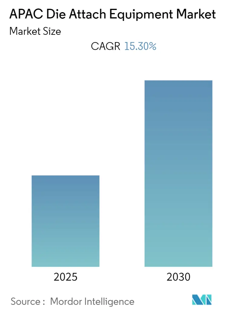
The APAC Die Attach Equipment Market is expected to register a CAGR of 15.3% during the forecast period.
- A significant focus for the next investment round by market vendors is developing die bonding and packaging solutions for smaller and highly complex 5G compatible smartphones. 5G is a unifying connectivity platform for future innovation, enabling continuous secure cloud access at significantly higher data and video transmission speeds.
- User adoption of 5G capabilities expands mobile broadband activities and accelerates artificial intelligence usage for the Internet of Everything. Likewise, the substrate and wafer-level packaging processes for mobile internet, computing, 5G, and automotive end-user applications drove the semiconductor industry to see a recovery in capital investment for memories and logic.
- The company has shared plans for a medium-to-long-term increase in capital investment towards expanded semiconductor and FPD applications. Whereas, as per Shibaura, active development of high-speed, high-precision bonding equipment for FOWLP / PLP and μLED is being looked out for in semiconductor assembly equipment.
- BESI has shared plans to invest in new assembly technologies such as FOWLP, TCB, TSV, ultra-thin dies, hybrid bonding, large area, wafer level molding, solar, and 3D-lithium-ion battery plating for the new digital society. Its lineup under Die attach equipment includes a single chip, multi-chip, multi-module, flip chip, TCB, FOWLP, hybrid die bonding systems, and die sorting systems.
- However, one source of concern is the continuing uncertain outlook due to the impact of the global spread of COVID-19. Lockdowns and production halts across Asia-pacific due to the COVID-19 outbreak had significantly impacted the production and consumption of semiconductors. With the majority of the IDS and foundries located in the region, the impact of shutdowns has led to reduced spending on capital investments. This is likely to impact the market studied, with a slowed recovery expected across 2021.
APAC Die Attach Equipment Market Trends and Insights
CIS is expected to witness significant growth
- CMOS image sensors have been offering camera functions in smartphones and other products, and as the scaling demand grows, the related manufacturing issues in the fab arise.
- The higher-bandwidth data performance progressed from 3G to 4G, and currently, to 5G, the demand for higher quality cameras has grown. This trend has propelled the CMOS image sensor stacking techniques based on the need for higher pixel counts and better resolution. Beyond these trends, the areas of biometric ID, 3D sensing, and enhanced human vision applications have augmented segment growth.
- Customer demand for bigger and better cameras results in more sensors with bigger die sizes. Besides pixel scaling, CMOS image sensors are undergoing other innovations like die stacking. Vendors in the market studied are also using different interconnect technologies, such as through-silicon vias (TSVs), hybrid bonding, and pixel-to-pixel for the same.
- In hybrid bonding, for instance, the dies are connected using copper-to-copper interconnects. For this, two wafers are processed in a fab. One is the logic wafer, while the other is the pixel array wafer. The two wafers are joined using a dielectric-to-dielectric bond, followed by a metal-to-metal connection.
- Hybrid bonding DBI technologies, Xperi'sproprietary technology, are being significantly used by Samsung towards CMOS image sensor fabrication for its phones. This technology for CMOS Image Sensors facilitates room temperature Cu-Cu permanent bonding, low-temperature annealing (around 300°C) & no external pressure bonding process (dielectric/metal).
- Prior to this, direct bond technology has thus played an enabling role in the realization of pixel scaling (backside illumination) BSI and stacked BSI with multiple generational variations led by Xperifor over 15 years.
LED to dominate market share
- Die attach material represents a key role in the performance and reliability of mid, high, and super-high power LEDs. The demand for die-attach equipment is increasing with an increasing LED penetration rate. The selection of suitable die-attach material for a particular chip structure and application depends on various considerations, which include the packaging process (throughput and yield), performance (thermal dissipation output and light output), reliability (lumen maintenance), and cost. Eutectic gold-tin, silver-filled epoxies, solder, silicones, and sintered materials have all been used for LED die attach.
- SFE provides an Epoxy Adhesive bonding method where its LED Epoxy Die Bonder machine features an index time of 0.2 Sec /Cycle (90 Percent Rate of Operation) with a chip size of 250 * 250 standards, providing lead frame recognition through 2 Cameras. Its software function provides auto mount level & pick up level teaching functions.
- Further, conductive adhesives (mostly silver-filled epoxies) constitute the largest class of thermal die-attach materials (by unit number) for LEDs. They are compatible with existing back-end packaging equipment and provide an attractive cost/performance balance (typically up to 50 W/mK thermals with secondary reflow compatibility). As they stick to bare silicon, they are the most preferred material for dies without back-end metallization like GaN on silicon.
- Further, in the LED market, there are a lot of rival competitors, and ASM is one of the prominent players in this market; its LED Epoxy High speed die bonder AD830 dominates in the LED market. It is fast, reliable, and accurate with die placement accuracy of +/-1 mil and +/-3 degree, cycle time for a small chip like 10mil x 10mil is 180 ms, which is an equivalent UPH of 18,000. It is equipped with a Post bond inspection system that monitors the bonded unit at the pre-set placement range.
Competitive Landscape
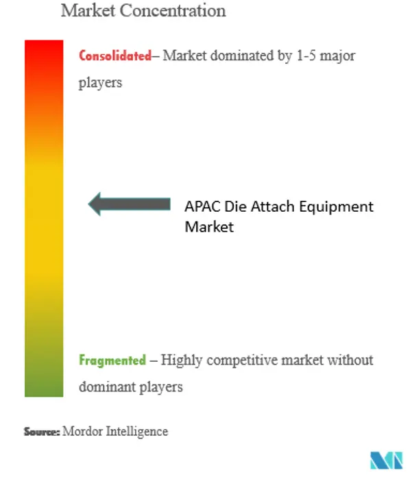
The APAC Die attach equipment market is moderately competitive, with a large number of players having a small market share. The companies keep innovating and entering into strategic partnerships to maintain their market share.
- April 2022 - Driving the Electric Revolution Industrialization Centre (DER-IC) North East has received equipment from Inseto, a top technical distributor of tools and materials, to improve its power electronics, machines, and drives (PEMD) capabilities. The first micro-punch machine to be installed in the UK is an AMX P100 sinter press, which is part of the equipment provided and will allow the production of high-reliability, high-power modules.
- June 2022 - The new 7KF Bonder Series has been developed by West Bond. This well-known company designs and manufactures a line of wire bonding and die-to-attach machines, wire pull and shear test equipment, ultrasonic components, and accessories for the microelectronics packaging industry. This excellent tool is made to handle the difficult bonding applications found in the RF, microwave, semiconductor, hybrid, and medical device fields.
APAC Die Attach Equipment Industry Leaders
-
Palomar Technologies, Inc.
-
Shinkawa Ltd.
-
Panasonic Corporation
-
ASM Pacific Technology Limited
-
Be Semiconductor Industries N.V.
- *Disclaimer: Major Players sorted in no particular order
Recent Industry Developments
- July 2022 - A major advancement in die-to-wafer (D2W) fusion and hybrid bonding has been made, according to EV Group (EVG), a provider of wafer bonding and lithography equipment for the MEMS, nanotechnology, and semiconductor markets. This was accomplished by successfully demonstrating 100 percent void-free bonding yield of multiple dies of various sizes from a full 3D system-on-a-chip (SoC) in a single transfer process using EVG's GEMINI. Up until now, achieving such a feat had been a huge difficulty for D2W bonding and a significant roadblock to lowering the cost of heterogeneous integration implementation.
- July 2022 - Using the first HBM3 samples made public by SK Hynix, Global Unichip Corp. (GUC), a leading Advanced ASIC, revealed that their 7.2 Gbps HBM3 solution has been silicon-proven. The platform was displayed in the Partner Pavilion at the TSMC 2022 North America Technology Symposium. It featured an HBM3 Controller, a PHY, a GLink-2.5D die-to-die interface, and a 112G SerDes. Both the TSMC CoWoS-S (silicon interposer) and CoWoS-R (organic interposer) advanced platform supports packaging technologies.
APAC Die Attach Equipment Market Report Scope
Die attach is a crucial process in semiconductor packaging. It covers all devices across various applications and contributes to assembly costs. Die bonding is a manufacturing process used in the packaging of semiconductors. It is the act of attaching a die (or chip) to a substrate or package by epoxy or solder, also known as die placement or die attach.
The market is segmented by Technique (Die bonder(Epoxy/Adhesive, Eutectic, Solder, Sintering), Flip chip bonder(Pick and Place/reflow soldering, Thermocompression, Thermosonic Bonding, Hybrid Bonding)), Application (Memory, LED, Logic, CMOS Image Sensor(CIS), Optoelectronics/Photonics, Discrete Power Devices, MEMS & Sensors, Stacked Memory & RF), and Country (Taiwan, China, Japan, Korea, Southeast Asia).
| Die Bonder | Epoxy/Adhesive (paste/film) |
| Eutectic | |
| Solder | |
| Sintering | |
| Flip Chip Bonder | Pick and Place / reflow soldering |
| Thermocompresion (TCB) | |
| Thermosonic Bonding | |
| Hybrid Bonding |
| Memory |
| LED |
| Logic |
| CMOS Image Sensor |
| Optoelectronics / Photonics |
| Discrete Power Devices |
| MEMS & Sensors |
| Stacked Memory & RF |
| Taiwan |
| China |
| Japan |
| Korea |
| Southeast Asia |
| By Bonding Technique | Die Bonder | Epoxy/Adhesive (paste/film) |
| Eutectic | ||
| Solder | ||
| Sintering | ||
| Flip Chip Bonder | Pick and Place / reflow soldering | |
| Thermocompresion (TCB) | ||
| Thermosonic Bonding | ||
| Hybrid Bonding | ||
| Application | Memory | |
| LED | ||
| Logic | ||
| CMOS Image Sensor | ||
| Optoelectronics / Photonics | ||
| Discrete Power Devices | ||
| MEMS & Sensors | ||
| Stacked Memory & RF | ||
| Country | Taiwan | |
| China | ||
| Japan | ||
| Korea | ||
| Southeast Asia | ||
Key Questions Answered in the Report
What is the current APAC Die Attach Equipment Market size?
The APAC Die Attach Equipment Market is projected to register a CAGR of 15.3% during the forecast period (2025-2030)
Who are the key players in APAC Die Attach Equipment Market?
Palomar Technologies, Inc., Shinkawa Ltd., Panasonic Corporation, ASM Pacific Technology Limited and Be Semiconductor Industries N.V. are the major companies operating in the APAC Die Attach Equipment Market.
What years does this APAC Die Attach Equipment Market cover?
The report covers the APAC Die Attach Equipment Market historical market size for years: 2019, 2020, 2021, 2022, 2023 and 2024. The report also forecasts the APAC Die Attach Equipment Market size for years: 2025, 2026, 2027, 2028, 2029 and 2030.
Page last updated on:
APAC Die Attach Equipment Market Report
Statistics for the 2025 APAC Die Attach Equipment market share, size and revenue growth rate, created by Mordor Intelligence™ Industry Reports. APAC Die Attach Equipment analysis includes a market forecast outlook for 2025 to 2030 and historical overview. Get a sample of this industry analysis as a free report PDF download.
