Market Size of Advanced Packaging Industry

| Study Period | 2019 - 2029 |
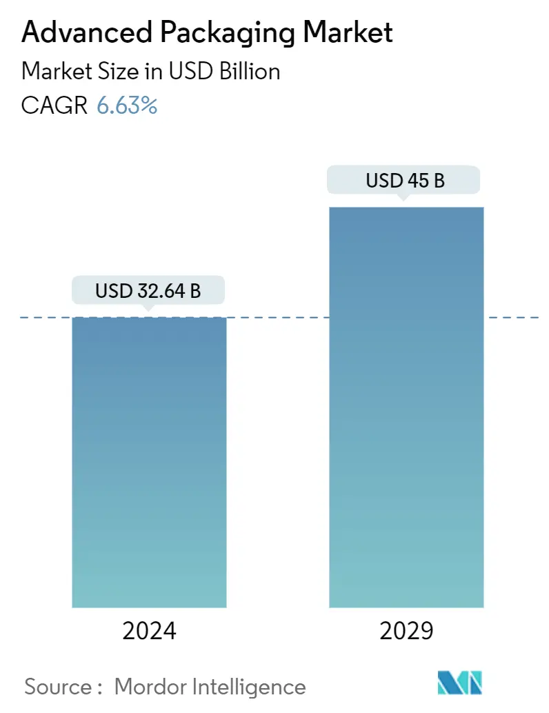
| Market Size (2024) | USD 32.64 Billion |
| Market Size (2029) | USD 45 Billion |
| CAGR (2024 - 2029) | 6.63 % |
| Fastest Growing Market | Asia Pacific |
| Largest Market | Asia Pacific |
| Market Concentration | Medium |
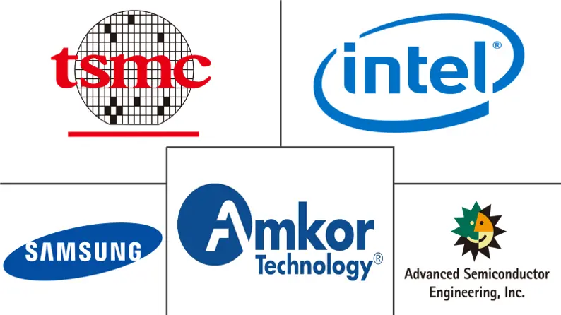
Major Players
*Disclaimer: Major Players sorted in no particular order |
Advanced Packaging Market Analysis
The Advanced Packaging Market size is estimated at USD 32.64 billion in 2024, and is expected to reach USD 45 billion by 2029, growing at a CAGR of 6.63% during the forecast period (2024-2029).
- Advanced packaging refers to the aggregation and interconnection of components before traditional integrated circuit packaging. It allows multiple devices, such as electrical, mechanical, or semiconductor components, to be merged and packaged as a single electronic device. Unlike traditional integrated circuit packaging, advanced packaging employs processes and techniques that are performed at semiconductor fabrication facilities. It sits in between fabrication and traditional packaging, and it includes various technologies like 3D ICs, 2.5D ICs, fan-out wafer-level packaging, system-in-package, etc.
- Advanced packaging can achieve performance gains through the integration of multiple chips in a package. By connecting these chips using fatter, such as through-silicon vias, interposers, bridges, or simple wires, the speed of signals can be increased, and the amount of energy required to drive those signals can be reduced. Additionally, advanced packaging allows for the mixing of components developed at different process nodes.
- Advanced packaging techniques, such as 3D integration and heterogenous integration, can significantly improve the performance of integrated circuits and memory chips. These techniques allow for increased feature density, interconnect density, and customization of memory for specific applications. For instance, memory-integrated device manufacturers (IDMs) can use 3D stacking technology to enhance performance in memory chips and customize memory for specific clients.
- Advanced packaging techniques also enable the reduction of the size of electronic components without compromising their performance. Simulation tools and Multiphysics approaches are used in advanced packaging to assess and ensure the thermal reliability and signal integrity of designs. By identifying potential packaging problems early in the design phase, integrated circuit designers can make modifications to improve reliability before prototyping.
- The experience of the global financial crisis changes to regulatory frameworks and the post-crisis market environment has had a significant impact on the advanced packaging market. To remain competitive in the market, OSATs are increasing their M&A activities. This will continue throughout the coming years, with various levels of consolidation among the major players.
- The consolidation will increase as chipmakers are already grappling with the increasing complexity, the loss of a roadmap for future designs as Moore’s Law is becoming more difficult and expensive to sustain, and a flood of new markets with evolving standards and different sets of rules. Acquisitions can have a big impact on product support and servicing of the existing technology. This is particularly troublesome for markets in which the devices are expected to function for about 10 to 20 years. This is expected to restrain the growth of the market..
Advanced Packaging Industry Segmentation
Advanced packaging refers to the aggregation and interconnection of components before traditional integrated circuit packaging. It allows multiple devices, such as electrical, mechanical, or semiconductor components, to be merged and packaged as a single electronic device. Unlike traditional integrated circuit packaging, advanced packaging employs processes and techniques at semiconductor fabrication facilities.
The advanced packaging market is segmented by packaging platform and geography. By packaging platform market is segmented into flip chip, embedded die, Fi-WLP, Fo-WLP, and 2.5D/3D. By geography, the market is segmented into North America, Europe, Asia Pacific, Latin America, and the Middle East and Africa.
The report offers market forecasts and size in value (USD) for all the above segments.
| By Packaging Platform | |
| Flip Chip | |
| Embedded Die | |
| Fi-WLP | |
| Fo-WLP | |
| 2.5D/3D |
| By Geography*** | |
| North America | |
| Europe | |
| Asia | |
| Australia and New Zealand | |
| Latin America | |
| Middle East and Africa |
Advanced Packaging Market Size Summary
The advanced packaging market is poised for significant growth, driven by the increasing demand for high-performance electronic devices and the integration of advanced technologies. This market encompasses various techniques such as 3D ICs, 2.5D ICs, and system-in-package solutions, which enhance the performance and efficiency of integrated circuits and memory chips. These technologies enable the integration of multiple chips into a single package, improving signal speed and reducing energy consumption. The market is also influenced by the need for miniaturization in consumer electronics and the adoption of 5G networks, which require compact and efficient devices. As a result, advanced packaging solutions are becoming essential in sectors like telecommunications, automotive, and consumer electronics, where they offer benefits such as increased functionality, reduced size, and improved reliability.
The Asia Pacific region is expected to dominate the advanced packaging market due to its robust semiconductor manufacturing base and rapid industrialization. Countries like China and Taiwan are making substantial investments to enhance their semiconductor industries, driven by the demand for advanced packaging technologies. These investments are aimed at achieving self-sufficiency in chip production and meeting the growing needs of the global market. The region's focus on developing advanced packaging solutions is further supported by private sector investments and government initiatives, positioning it as a key player in the global semiconductor packaging landscape. As the market continues to evolve, major players are engaging in strategic collaborations and investments to strengthen their positions and capitalize on emerging opportunities.
Advanced Packaging Market Size - Table of Contents
-
1. MARKET INSIGHTS
-
1.1 Market Overview
-
1.2 Industry Value Chain Analysis
-
1.3 Industry Attractiveness - Porter's Five Forces Analysis
-
1.3.1 Threat of New Entrants
-
1.3.2 Bargaining Power of Buyers
-
1.3.3 Bargaining Power of Suppliers
-
1.3.4 Threat of Substitute Products
-
1.3.5 Intensity of Competitive Rivalry
-
-
1.4 Assessment of the Impact of COVID-19 and Macro Economic Trends on the Industry
-
-
2. MARKET SEGMENTATION
-
2.1 By Packaging Platform
-
2.1.1 Flip Chip
-
2.1.2 Embedded Die
-
2.1.3 Fi-WLP
-
2.1.4 Fo-WLP
-
2.1.5 2.5D/3D
-
-
2.2 By Geography***
-
2.2.1 North America
-
2.2.2 Europe
-
2.2.3 Asia
-
2.2.4 Australia and New Zealand
-
2.2.5 Latin America
-
2.2.6 Middle East and Africa
-
-
Advanced Packaging Market Size FAQs
How big is the Advanced Packaging Market?
The Advanced Packaging Market size is expected to reach USD 32.64 billion in 2024 and grow at a CAGR of 6.63% to reach USD 45 billion by 2029.
What is the current Advanced Packaging Market size?
In 2024, the Advanced Packaging Market size is expected to reach USD 32.64 billion.

