Advanced IC Substrates Market Size and Share
Market Overview
| Study Period | 2020 - 2031 |
|---|---|
| Market Size (2026) | USD 11.37 Billion |
| Market Size (2031) | USD 15.67 Billion |
| Growth Rate (2026 - 2031) | 6.63% CAGR |
| Fastest Growing Market | North America |
| Largest Market | Asia Pacific |
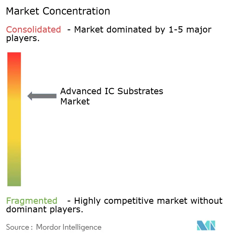
| Market Concentration | Medium |
Major Players *Disclaimer: Major Players sorted in no particular order Image © Mordor Intelligence. Reuse requires attribution under CC BY 4.0. | |
Advanced IC Substrates Market Analysis by Mordor Intelligence
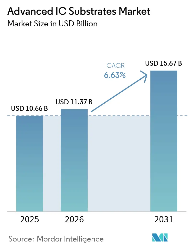
The advanced IC substrates market size is expected to grow from USD 10.66 billion in 2025 to USD 11.37 billion in 2026 and is forecast to reach USD 15.67 billion by 2031 at a 6.63% CAGR over 2026-2031. Surging demand for artificial-intelligence accelerators is forcing substrate suppliers to tighten line-and-space geometries below 10 micrometers, a capability concentrated among four Taiwanese and Japanese vendors. Intensifying sovereign-AI policies in the European Union and India are lengthening delivery cycles, while the North American CHIPS Act grants are creating new capacity but also fragmenting order volumes. Glass cores are gaining traction at sub-4-nanometer logic nodes, yet Ajinomoto build-up film retains incumbency in mainstream devices. Competitive leverage, therefore, pivots on yield, flatness, and collaborative engineering rather than pure pricing, keeping the advanced IC substrates market structurally tight through the forecast horizon.
Key Report Takeaways
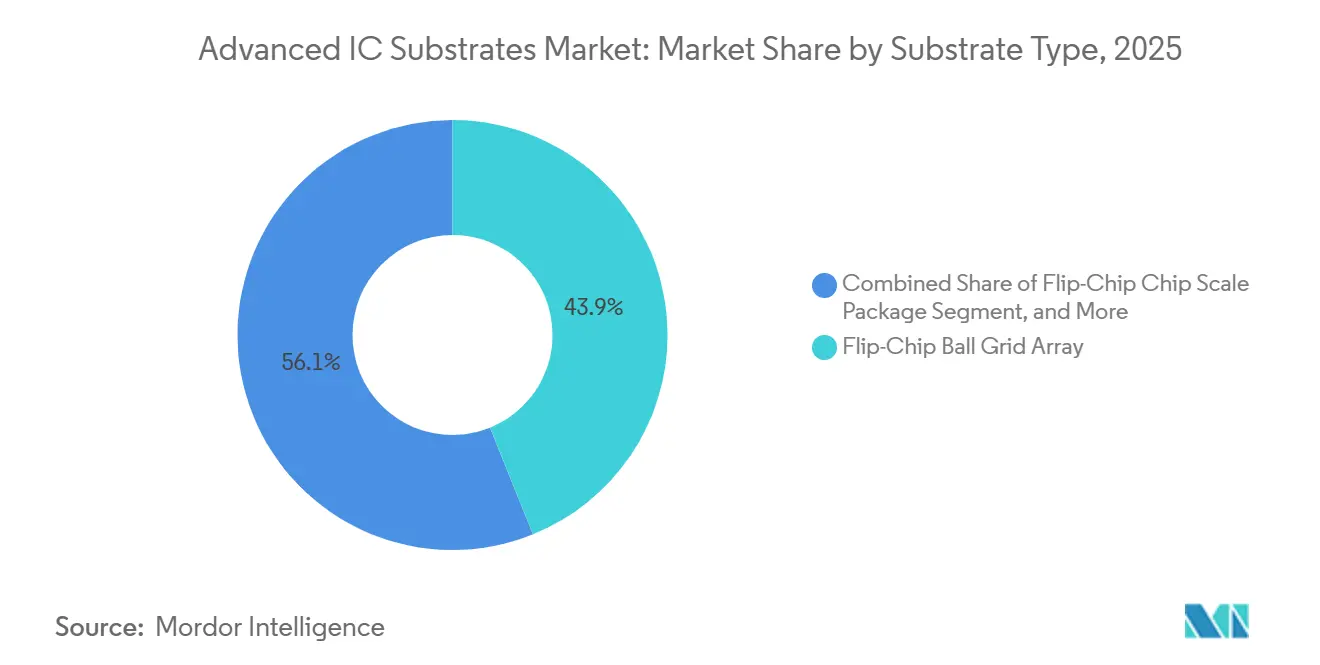
- By substrate type, flip-chip BGA led with 43.89% revenue share in 2025, while rigid-flex and flexible CSP are forecast to expand at a 7.71% CAGR through 2031.
- By core material, Ajinomoto build-up film accounted for 52.78% of the advanced IC substrates market share in 2025, whereas glass substrates are projected to grow at a 7.47% CAGR through 2031.
- By packaging technology, 2D flip-chip held 39.91% of 2025 revenue, while 3D-IC architectures are poised for a 7.66% CAGR over 2026-2031.
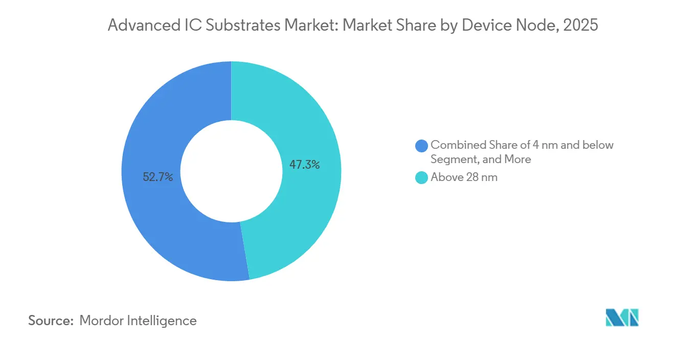
- By device node, products fabricated above 28 nanometers accounted for 47.33% of the advanced IC substrates market share in 2025, whereas 4-nanometer and below devices are set to deliver a 7.43% CAGR to 2031.
- By end-use industry, mobile and consumer applications represented 36.19% of the advanced IC substrates market share in 2025, while data-centre, AI, and HPC substrates are advancing at a 7.61% CAGR through 2031.
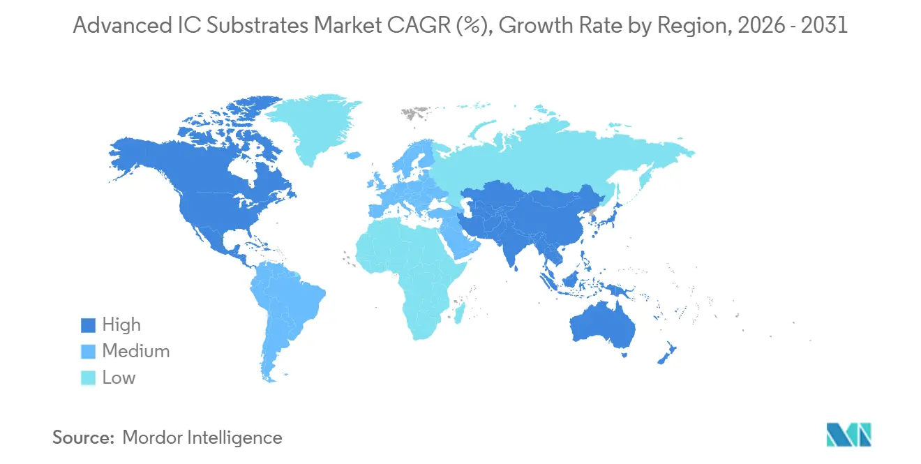
- By geography, Asia-Pacific dominated with a 78.36% share in 2025, whereas North America is projected to rise at a 7.69% CAGR during 2026-2031.
Note: Market size and forecast figures in this report are generated using Mordor Intelligence’s proprietary estimation framework, updated with the latest available data and insights as of 2026.
Global Advanced IC Substrates Market Trends and Insights
Drivers Impact Analysis*
| Driver | (~) % Impact on CAGR Forecast | Geographic Relevance | Impact Timeline |
|---|---|---|---|
| Surge in ABF-substrate demand for AI and HPC accelerators | +1.8% | Global, concentration in North America and Asia-Pacific | Medium term (2-4 years) |
| Miniaturisation and heterogeneous integration trend | +1.5% | Global, led by Taiwan, South Korea, United States | Long term (≥ 4 years) |
| 5G roll-out boosting high-frequency RF packaging | +1.0% | Asia-Pacific core, spill-over to Europe and North America | Short term (≤ 2 years) |
| Co-packaged optics adoption requiring ultra-low-loss substrates | +0.9% | North America and Europe data-centre hubs | Long term (≥ 4 years) |
| CHIPS-style localisation subsidies tied to substrate fabs | +0.7% | United States, European Union, Japan, India | Medium term (2-4 years) |
| Large-panel organic substrate lines lowering cost per die | +0.6% | Asia-Pacific manufacturing clusters | Medium term (2-4 years) |
| Source: Mordor Intelligence | |||
Surge in ABF-Substrate Demand for AI and HPC Accelerators
Hyperscale operators installed more than 1.2 million AI accelerator units in 2025, each integrating four to six flip-chip BGA substrates that must withstand power draw above 700 watts.[1]NVIDIA Corporation, “Form 10-K 2025,” nvidia.com Average selling prices climbed from USD 65 in 2024 to USD 82 in 2025 as coating-line additions lagged demand, widening suppliers' margins as they locked in Ajinomoto film allocations. Fabless chipmakers are now co-investing in substrate plants, illustrated by AMD’s USD 400 million venture with Siliconware Precision Industries that secures 30% of a new Taiwanese facility’s output. These forward-buy agreements squeeze mid-tier vendors that lack guaranteed slots, reinforcing a capacity oligopoly. As long as accelerator shipments double every 2 years, the advanced IC substrates market will continue to absorb incremental ABF panels at premium pricing.
Miniaturisation and Heterogeneous Integration Trend
Chiplet architectures slice monolithic dies into smaller compute, I/O, and memory tiles, cutting die area by up to 40% and enabling node-mixing strategies. Such layouts demand microvias below 50 micrometers and redistribution layers at 2 micrometer pitch, pushing both ABF and emerging glass cores to their physical limits.[2]IEEE, “IEDM Proceedings 2025,” ieee.org To stay design-win-relevant, Ibiden and AT&S embedded engineers at TSMC’s packaging center 18 months ahead of tape-out, capturing 40% of the 2.5D interposer substrate pool by 2025. The collaboration model shifts substrate manufacturing from commodity production toward quasi-design services, accelerating learning curves and deepening vendor lock-in. Over the next decade, suppliers unable to align roadmaps with foundries risk relegation to legacy nodes, curtailing addressable revenue in the advanced IC substrates market.
5G Roll-Out Boosting High-Frequency RF Packaging
Millimeter-wave 5G smartphones and base stations operate above 24 gigahertz, requiring dielectric constants below 3.5 and dissipation factors under 0.005 to curb signal loss. When Qualcomm’s Snapdragon X80 modem integrated on-package antenna arrays in early 2025, unit volumes for rigid-flex substrates jumped 35% year-on-year and lowered average prices to USD 8 as panel utilization improved.[3]Qualcomm Incorporated, “Q4 2025 Earnings Call,” qualcomm.com Compliance with IEC 62232 and FCC Part 15 emissions standards now compels substrate vendors to invest in in-house RF test chambers or face four-to-six-week qualification delays. These dynamics accelerate material migration toward liquid-crystal polymer and reinforced polyimide, stimulating incremental revenue even as handset volumes plateau. The spill-over into small-cell infrastructure broadens geographic exposure beyond Asia-Pacific, keeping the advanced IC substrates market diversified across end uses.
Co-Packaged Optics Adoption Requiring Ultra-Low-Loss Substrates
Data-centre switches targeting 1.6 terabits per second are moving optical engines from pluggable modules onto the ASIC package to save 5-8 watts per lane. Glass cores with matched refractive indices permit waveguide routing while holding insertion loss below 0.5 dB per centimeter, a benchmark organic ABF cannot meet. Amazon, Google, and Meta have funded pilot lines at Corning and AGC, absorbing the USD 300-400 unit premium in exchange for lower rack-level power. Suppliers without glass competence risk exclusion from next-generation switch sockets, concentrating future revenue among a handful of specialists. The resulting bifurcation could lift blended ASPs even as volumes stay limited, adding a measured yet durable tailwind to the advanced IC substrates market.
Restraints Impact Analysis*
| Restraint | (~) % Impact on CAGR Forecast | Geographic Relevance | Impact Timeline |
|---|---|---|---|
| ABF-substrate capacity shortage and lead-time spikes | -1.2% | Global, acute in North America and Europe | Short term (≤ 2 years) |
| High capital intensity and process complexity | -0.9% | Global, barrier to entry in all regions | Long term (≥ 4 years) |
| Single-source dependency on ABF build-up films | -0.6% | Global supply chain | Medium term (2-4 years) |
| Stricter fluorinated-solvent emission regulations | -0.4% | North America and European Union | Medium term (2-4 years) |
| Source: Mordor Intelligence | |||
ABF-Substrate Capacity Shortage and Lead-Time Spikes
Lead times for 14-layer ABF substrates stretched to 28 weeks in early 2025 as AI demand outran supply by 18 percentage points. Mid-tier fabless designers either paid spot premiums of 15-20% or postponed tape-outs by up to three quarters. Equipment chokepoints persist: LPKF Laser and Mitsubishi Electric hold roughly 70% of laser-drill capacity and face an 18-month delivery backlog. Large suppliers, therefore, over-book Ajinomoto film, amplifying scarcity for smaller rivals. Unless new coating lines come online before 2027, the advanced IC substrates market will remain capacity-constrained, trimming potential CAGR by an estimated 1.2 percentage points.
High Capital Intensity and Process Complexity
A 50,000-panel-per-month FC-BGA plant costs USD 800 million -1 billion and needs 30-36 months to qualify, deterring fresh entrants. Fourteen-layer flows involve more than 60 manufacturing steps with cumulative yields near 75-80%, so one in four panels is scrapped. Only vertically integrated players with strong cash reserves can absorb prolonged negative free cash flow. Capital scarcity explains why 2024-2025 capacity expansions came exclusively from incumbent brownfield sites, perpetuating pricing power. This structural hurdle subtracts almost a full percentage point from long-term growth in the advanced IC substrates market.
*Our forecasts treat driver/restraint impacts as directional, not additive. The impact forecasts reflect baseline growth, mix effects, and variable interactions.
Segment Analysis
By Substrate Type: Flip-Chip BGA Dominance and Rigid-Flex Momentum
Flip-chip BGA commanded 43.89% of the advanced IC substrates market share in 2025, reflecting its entrenched position in mobile application processors and server CPUs. Rigid-flex and flexible CSP formats are advancing at a 7.71% CAGR through 2031, driven by smartwatches, augmented-reality headsets, and medical patches that benefit from bendable polyimide cores. Flip-chip CSP held 22% of 2025 shipment volume for ultra-thin smartphones, while organic BGA and LGA accounted for a steady 18% of volume in cost-focused automotive controllers. Other formats, including embedded-die and coreless substrates, accounted for the remaining 16%, driven by 5G millimeter-wave front-end modules that require improved thermal paths.
Chiplet-ready flip-chip BGA variants command 25-35% ASP premiums because multi-cavity layouts and fine redistribution layers raise manufacturing complexity. Suppliers with laser-direct-imaging and modified semi-additive processes secured roughly 70% of this high-margin pool, reshaping competitive balance. By contrast, panel-level processing helped rigid-flex yields, but the resulting 5% ASP erosion in 2025 pressured specialists to consolidate. The technology mix, therefore, tilts profitability toward advanced flip-chip formats even as unit growth skews toward flexible substrates, keeping product strategy nuanced across the advanced IC substrates market.


By Core Material: ABF Incumbency, Glass Upswing
Ajinomoto build-up film captured 52.78% of 2025 revenue, reinforcing its status as the incumbent core for smartphones, PCs, and servers. Glass substrates are set for a 7.47% CAGR through 2031 as sub-4-nanometer logic and co-packaged optics demand ultra-low warpage and optical routing. Bismaleimide-triazine accounted for 15% of the volume in high-temperature automotive modules, while ceramic remained at 9% for RF power and LED packages. Hybrid glass-organic laminates under development could combine cost efficiency with glass-level flatness, challenging pure ABF beyond 2027.
Hyperscaler funding for Corning and AGC pilot lines may lift glass to 15-20% of premium server sockets by 2031, injecting fresh revenue into the advanced IC substrates market size. Automotive price-down pressure of 2-3% a year forces BT and ceramic vendors to automate inspection and test to protect margins. As a result, the long-term material strategy hinges on balancing ABF volume, glass performance, and BT cost discipline across diversified end uses.
By Packaging Technology: 2D Maturity and 3D-IC Lift
2D flip-chip held 39.91% of 2025 revenue, favored for yields above 95% in mature mobile and GPU designs. 3D-IC and SoIC architectures are projected to grow at a 7.66% CAGR during 2026-2031, driven by stacked high-bandwidth memory on logic dies via hybrid bonding. 2.5D interposers retained 18% of revenue in data-center GPUs that require multi-terabit die-to-die bandwidth, while fan-out wafer-level packaging accounted for 14% in RF front-end modules. System-in-package and module formats filled the balance at 28%, led by automotive radar and telecom small-cell nodes.
Hybrid bonding tightens flatness tolerances below 2 micrometers, prompting investments in chemical-mechanical polishing and precision metrology. Organic interposers aim to break the 1 dB/cm loss barrier at 112 GHz by 2026, a milestone that could displace costlier silicon. Fan-out panel-level lines that reduce the cost per die by up to 20% will help penetrate the high-volume automotive power device market. These technology shifts diversify revenue streams while sustaining innovation premiums inside the advanced IC substrates market share landscape.
By Device Node: Legacy Volume and Leading-Edge Push
Devices above 28 nanometers generated 47.33% of 2025 revenue, underscoring the vast installed base of automotive and industrial electronics. Sub-4-nanometer designs are forecast to deliver a 7.43% CAGR, driven by AI accelerators and flagship smartphones that demand 8-micrometer line-and-space densities. The 16/14-10 nanometer cohort held 22% and continues to serve mid-range smartphones and networking ASICs, while 7-5 nanometer nodes accounted for 18% in server CPUs and discrete GPUs.
Power densities above 1.5 W/mm² at sub-4-nanometer nodes require embedded capacitors and robust power planes, inflating substrate ASPs by USD 15-25 per unit. Chinese rivals expanding at 16/14 nanometers undercut prices by 10-15%, commoditizing that tier and squeezing incumbent margins. Automotive legacy nodes remain protected by 24-36-month qualification cycles, giving established suppliers a moat even as advanced-node volumes climb. The node mix, therefore, balances stability and innovation within the advanced IC substrates market.
By End-Use Industry: Mobile Plateau, Data-Center Surge
Mobile and consumer products accounted for 36.19% of 2025 revenue, but smartphone unit volumes have leveled off at 1.2 billion annually. Data-center, AI, and HPC uses are advancing at a 7.61% CAGR, with hyperscalers ordering multi-substrate GPU modules that cost USD 150-200 apiece. IT and telecom infrastructure accounted for 24%, automotive for 18%, and industrial, medical, and aerospace for the residual 22%. Regional spending cycles in 5G and optical transport continue to shape demand swings for telecom-grade substrates.
A bifurcated data-center market has emerged: custom ASIC builders absorb premium glass or high-layer ABF substrates, while merchant silicon buyers stay with mainstream FC-BGA. Mobile revenue now grows through mmWave modules and under-display sensors rather than handset count. Automotive migration from alumina ceramic to organic core trims inverter costs by 30%, yet pressures ceramic revenue, prompting diversification into LED and RF niches. These cross-industry trends distribute growth drivers broadly, supporting resilience in the overall advanced IC substrates market share.
Geography Analysis
Asia-Pacific accounted for 78.36% of the advanced IC substrates market size in 2025, anchored by Taiwan’s 420 million flip-chip BGA shipments and Japan’s specialization in 14-layer and 16-layer server substrates. South Korean vendors raised rigid-flex output to 85 million units and achieved cost parity with strip formats by switching to panel processing. Chinese suppliers increased legacy-node capacity and priced 10-15% below Taiwanese averages, boosting their share of automotive and industrial demand to 18%. India remained a nascent player, as pilot lines at Tata Electronics and Kaynes Technology shipped fewer than 5 million substrates due to yield challenges.
North America is projected to expand at a 7.69% CAGR through 2031, propelled by USD 2.8 billion in CHIPS Act incentives tied to domestic substrate and packaging plants. Ibiden’s USD 1.2 billion Arizona fab and AT&S’s USD 800 million Texas facility will together add 50,000 panels per month after 2027, giving U.S. fabless firms a second sourcing hub. Mexican near-shoring added 22 million units in 2025 as Tripod Technology and Zhen Ding Technology enlarged Guadalajara operations to serve automotive and industrial customers. Dual-sourcing clauses in U.S. contracts are already fragmenting order volumes, pressuring Asian incumbents to establish North American subsidiaries to defend their share.
Europe accounted for 6% of 2025 revenue, concentrated in Austria and Germany, where AT&S and Schweizer Electronic cater to automotive and industrial clients. AT&S’s Leoben expansion, backed by EUR 500 million in EU Chips funds, will bring 20,000 additional FC-BGA panels per month starting in 2027. South America, the Middle East, and Africa together accounted for less than 2%, reflecting limited semiconductor assembly capacity and long payback periods for greenfield fabs. Unless subsidy frameworks emerge to offset high capital costs, these regions will remain fringe participants in the advanced IC substrates market.

Regulatory Landscape
Policy support and trade measures are increasingly intertwined with advanced packaging and substrate localization. In the United States, CHIPS Act-linked incentives and procurement rules are shaping sourcing decisions for substrates and related semiconductor content, with the FAR Council issuing a February 2026 Notice of Proposed Rulemaking to implement Section 5949 of the FY23 NDAA, which would restrict executive agencies from acquiring certain semiconductors from specified Chinese entities. In parallel, a January 2026 Federal Register action introduced a 25% ad valorem duty on certain advanced computing chips and derivative products, reinforcing supplier due diligence around product classification and origin documentation when substrates are embedded in downstream assemblies.
In Europe, regulatory and industrial-policy priorities continue to shift toward enabling first-of-a-kind capabilities in advanced manufacturing. The European Commission adopted a proposal for Chips Act 2.0 in June 2026, explicitly covering next-generation technologies and pilot lines that include advanced packaging and 3D integration, both of which directly draw on advanced IC substrates. Alongside localization programs, environmental compliance is also tightening, including controls on fluorinated solvent emissions referenced as a market restraint for substrate production in North America and the European Union.
Value Chain Analysis
The advanced IC substrate value chain runs from concentrated upstream materials through capital-intensive substrate fabrication, then into qualification-heavy integration with advanced packaging. Key inputs include Ajinomoto build-up film, specialty copper foils, and glass materials, with upstream supply showing notable concentration in Japanese suppliers for ABF film and for key reinforcement and copper foil inputs. In manufacturing, high-layer-count ABF substrates remain constrained by equipment and process bottlenecks, notably laser drilling and fine-line imaging, which keeps lead times elevated for premium substrate classes and supports multi-year capacity reservation and co-investment structures.
Downstream, substrate makers interface closely with foundries and OSATs as 2.5D/3D platforms (for example, CoWoS and EMIB-style architectures) still rely on the same substrate supply pool, limiting risk mitigation from packaging platform diversification alone. 2026 announcements point to continued supply-chain restructuring: Samsung Electro-Mechanics disclosed an April 2026 investment program to expand ABF substrate capacity across Sejong (South Korea) and Thai Nguyen (Vietnam), while Nan Ya PCB outlined a 2026 capex plan exceeding NT$10 billion to expand advanced substrate output for AI and HPC demand. On the supplier-customer linkage side, AT&S announced in June 2026 an expansion at Kulim (Malaysia), including fit-out and new construction for IC substrate cores and advanced PCBs, supported by agreements with AMD and another leading technology company, which illustrates a shift toward contracted demand backing for large-scale capacity additions.
Competitive Landscape
The top five suppliers, Unimicron, Ibiden, Nan Ya PCB, Shinko Electric, and AT&S, controlled roughly 60% of global capacity in 2025, yet none exceeded an 18% individual share, preserving a moderately competitive environment. Multi-year contracts with hyperscalers include dual-source clauses that cap annual price increases at 3%, compelling vendors to compete on cycle time, yield, and co-design services rather than headline pricing. Unimicron bought a 30% stake in Corning’s glass pilot line for USD 180 million to secure next-generation core material, while Ibiden committed USD 1.2 billion to its Arizona facility to lock Intel and AMD volumes under domestic content rules.
Chinese challengers Shennan Circuits and Zhejiang Kingdom Sci-Tech expanded legacy-node output in 2025, pricing 10-15% below Japanese and Taiwanese peers and capturing 18% of automotive and industrial orders. Technology investment remains the primary moat, as suppliers that installed laser-directed imaging and modified semi-additive processes now handle most chiplet substrates with line widths under 8 micrometers. Ibiden’s 47 substrate patents filed in 2025, 60% of which are related to embedded capacitors and hybrid glass-organic cores, illustrate the intellectual property race that underpins differentiation.
Mid-tier firms continue to consolidate to fund capital-intensive upgrades. Flexium acquired Career Technology to gain scale in rigid-flex and negotiate improved polyimide pricing, while Daeduck Electronics divested strip-based lines to concentrate on panel-level processing. Suppliers that lack resources for glass, panel, or hybrid bonding technologies risk relegation to commoditized tiers. As capital spending rises and technical thresholds tighten, the competitive field is likely to narrow further, reinforcing the current moderate concentration within the advanced IC substrates market.
Advanced IC Substrates Industry Leaders
Unimicron Technology Corp.
Ibiden Co., Ltd.
Nan Ya Printed Circuit Board Corp.
Shinko Electric Industries Co., Ltd.
AT&S Austria Technologie & Systemtechnik AG
- *Disclaimer: Major Players sorted in no particular order

Market Opportunities and Future Outlook
A central opportunity is building geographically diversified, customer-anchored high-end substrate capacity as AI/HPC demand tightens supply for high-layer-count FC-BGA and chiplet-ready designs. Corporate disclosures in 2026 show this investment pattern concentrating in Asia and in North America-linked supply chains: AT&S announced agreements with AMD and another technology company to invest up to EUR 2 billion to expand AI substrate production in Kulim, Malaysia (June 2026), and LG Innotek disclosed plans to begin building a USD 1 billion semiconductor substrate plant in Hai Phong, Vietnam (Q3 2026 start). These efforts align with the report context that capacity additions increasingly depend on long-term commitments and localization requirements.
Technology whitespace is also forming around panel-format and next-generation core materials where substrate performance limits constrain advanced packaging roadmaps. In June 2026, TSMC standardized CoPoS (Chip-on-Panel-on-Substrate) on a 310 x 310 mm panel format with CoWoS_L volume production underway, raising demand for substrate makers that can deliver panel-level flatness, warpage, and yield at scale. In parallel, industry work on glass core substrates continues through pilot and qualification activity to address organic-substrate limitations for large AI packages and co-packaged optics, supported by earlier CHIPS incentives such as the December 2024 Department of Commerce award (up to USD 75 million) to Absolics for glass substrate technology development in Georgia.
Recent Industry Developments
- June 2026: AT&S announced an expansion of its Kulim, Malaysia site, including fit-out of Plant 2 and new construction for IC substrate cores and advanced PCBs, supported by agreements with AMD and another leading technology company. The company emphasized more contracted, AI-oriented capacity and deeper customer-supplier integration in high-end substrates. It also reinforces Southeast Asia as a manufacturing hub for advanced substrate supply chains.
- February 2026: Ibiden announced a JPY 500 billion capital investment plan for its electronics business for fiscal years 2026 to 2028, including an additional investment of about JPY 280 billion centered on the Ohno Plant to expand high-performance IC package substrate capacity for AI and high-performance servers. The scale of spending targets the high-layer-count segment where lead times and yields drive competitive outcomes. The plan supports tighter collaboration with AI server and accelerator ecosystems that depend on premium FC-BGA substrates.
- October 2025: Ibiden held an opening ceremony for its Ohno Plant in Gifu Prefecture, positioning the site as a major production hub for AI server IC package substrates. Bringing the facility online helped broaden Ibiden’s manufacturing base for high-value substrate classes and supported customer qualification timelines. The expansion also highlighted how incumbents are adding capacity through large, specialized hubs rather than incremental line additions.


Research Methodology Framework and Report Scope
Market Definition and Coverage
The advanced IC substrates market covers the value of high density package substrate materials and substrate fabrication used to connect semiconductor dies to the rest of the system through an IC package, across major end-use electronics.
Scope exclusions: Excluded are standard rigid PCBs for board-level assembly, semiconductor wafers and front-end processing, and the value of fully packaged chips beyond the substrate portion.
Segmentation Overview
- By Substrate Type
- Flip-Chip Ball Grid Array
- Flip-Chip Chip Scale Package
- Organic Ball Grid Array / Land Grid Array
- Rigid-Flex and Flexible Chip Scale Package
- Other Substrate Types
- By Core Material
- Ajinomoto Build-up Film
- Bismaleimide-Triazine Resin
- Glass
- Ceramic
- By Packaging Technology
- 2D Flip-Chip
- 2.5D Interposer
- 3D-IC / SoIC
- Fan-Out WLP
- SiP / Module
- By Device Node
- Above 28 nm
- 16/14–10 nm
- 7–5 nm
- 4 nm and below
- By End-Use Industry
- Mobile and Consumer
- Automotive and Transportation
- IT and Telecom Infrastructure
- Data-Centre / AI and HPC
- Other End-Use Industries
- By Geography
- North America
- United States
- Canada
- Mexico
- South America
- Brazil
- Argentina
- Rest of South America
- Europe
- United Kingdom
- Germany
- France
- Italy
- Rest of Europe
- Asia Pacific
- China
- Japan
- India
- South Korea
- Rest of Asia Pacific
- Middle East and Africa
- Middle East
- United Arab Emirates
- Saudi Arabia
- Rest of Middle East
- Africa
- South Africa
- Egypt
- Rest of Africa
- Middle East
- North America
Data Sources, Market Sizing, and Validation
Desk Research
Desk work was used to set the factual base for the model and to avoid guessing on core demand signals. We mainly pulled public indicators tied to semiconductor packaging activity and substrate manufacturing, and then aligned definitions so the data could be used together.
Sources we referred to include items such as government trade statistics (import and export codes linked to electronic components), central bank and IMF FX series for currency normalization, and industrial production series from agencies such as the US Federal Reserve. We also used patent databases for packaging and substrate process trends, peer reviewed journals for line and material constraints, and trade association releases covering semiconductor equipment and packaging capacity. Company filings, investor presentations, and reputable press were then used to confirm product mix shifts and expansion timing. Where public disclosures were light, a paid subscription for company financials and patent search helped close gaps. These examples are not exhaustive, and many other public sources were also used for data collection, validation, and research clarification.
Primary Interviews and Surveys
Field inputs were collected from substrate makers, materials participants, packaging ecosystem specialists, and downstream electronics stakeholders, so our assumptions were not built only on published data. We used these conversations to test adoption timing for advanced packages, sanity check pricing direction, and confirm where constraints or qualification cycles were actually limiting shipments across APAC, EMEA, and the Americas.
Distribution of primary research fieldwork respondents
| Company type | Respondent position | Region |
|---|---|---|
| Top tier: 27% | CXOs: 14% | APAC: 52% |
| Mid tier: 53% | Functional/Unit leaders: 41% | EMEA: 30% |
| Smaller Players: 20% | Managers: 45% | Americas: 18% |
Market-Sizing & Forecasting
Sizing starts with a top-down build where semiconductor packaging demand is reconstructed using end-use device shipments and mix shifts toward advanced packages, and then converted into substrate value using packaging intensity and typical substrate content per package. After that, selective bottom-up approximations are used, such as sampling average selling price bands by substrate type and combining them with shipment proxies from capacity and utilization checks, which helps adjust totals when the first pass looks stretched.
Inputs that materially move the model include the share of FC-BGA and FC-CSP in total advanced packages, ABF versus other core material penetration, substrate layer count and line width related complexity (which impacts price), utilization and yield direction at substrate lines, and the demand pull from data-center AI and HPC versus mobile and automotive electronics. Because pricing can move quickly, we also account for currency timing and regional ASP differences when a large part of supply is in Asia.
For forecasting, scenario analysis is used around capacity additions, qualification lead times, and end-market cycles, and the scenario weights are cross-checked with what interviewees see for ramp schedules. Where bottom-up details are incomplete for smaller producers, gaps are handled through calibrated ratios tied to regional capacity shares and observed ASP ranges, then rechecked against the top-down demand pool so the final path stays realistic.
Data Validation & Update Cycle
Validation is done by comparing the final market totals against independent signals that should move in the same direction, such as advanced packaging investment cycles, substrate capacity expansion announcements, and trade flow patterns for related electronic components. If a region or year shows an unusual jump, the assumptions are reviewed again, and follow-up outreach is triggered to confirm whether the change is real or a modeling artifact.
Before sign-off, the model is reviewed in steps, starting with unit and price logic checks, followed by region split checks, and then an overall reasonableness pass against historical patterns. The report is refreshed annually, and interim updates are made when major capacity starts, demand shocks, or policy shifts materially change the outlook. Right before delivery, a final update pass is completed so clients receive the latest version of the dataset and assumptions.
Mordor Intelligence's Advanced Ic Substrates Market Size Compared With Other Published Estimates
Published market sizes for advanced IC substrates often do not match because the underlying studies do not count the same things in the same way. Differences usually come from what substrate types are included, which years are treated as the current market, and how pricing is carried forward when product complexity is rising.
A second driver is the choice of demand anchor. Some estimates lean heavily on announced capacity or aggressive AI server growth, while others stay conservative and do not fully reflect substrate content growth in advanced packages. Currency conversion timing and refresh cadence can also shift a USD value by a noticeable margin, especially when the supply base is concentrated in Asia.
Benchmark comparison
| Source | Market Size | Gaps in Research Methodology |
|---|---|---|
| Mordor Intelligence | USD 11.37 B (2026) | |
| Global Research Publisher A | USD 16.73 B (2024) | Uses an earlier base year and often applies a higher near-term adoption curve for heterogeneous integration, which can pull forward value before qualification and yield ramps stabilize. |
| Industry Research Group B | USD 17.60 B (2026) | Tends to include a wider set of high-density substrate formats and adjacent substrate-like structures in the same value pool, which raises the counted dollar content per package. |
The table shows that scope and timing choices explain most of the spread, along with how quickly complexity-driven ASP is allowed to rise. By separating core IC package substrates from adjacent board-level and hybrid structures, and then validating the resulting totals against packaging mix and capacity utilization checks, the estimate stays closer to a repeatable demand pool, a treatment applied by Mordor Intelligence.


Key Questions Answered in the Report
What is the current and projected value of the advanced IC substrates market?
The advanced IC substrates market size is projected to rise from USD 11.37 billion in 2026 to USD 15.67 billion by 2031, reflecting a 6.63% CAGR.
Which substrate type holds the largest revenue share?
Flip-chip BGA substrates led the field with 43.89% of 2025 revenue.
Which region is growing fastest for advanced IC substrates?
North America is set to expand at a 7.69% CAGR through 2031, boosted by CHIPS-Act incentives.
Why are glass substrates gaining importance?
Glass cores provide ultra-low warpage and optical routing needed for sub-4-nanometer devices and co-packaged optics, driving a 7.47% CAGR.
What is the main capacity bottleneck facing the market?
Limited ABF film coating and laser-drilling equipment has extended lead times to 28 weeks, constraining supply.
How concentrated is supplier power in this market?
The top five companies hold around 60% of capacity, resulting in moderate concentration and competitive yet disciplined pricing.
Page last updated on: