
3D TSV Devices Market Size and Share
Market Overview
| Study Period | 2020 - 2031 |
|---|---|
| Market Size (2026) | USD 7.74 Billion |
| Market Size (2031) | USD 10.39 Billion |
| Growth Rate (2026 - 2031) | 6.06 % |
| Fastest Growing Market | Asia Pacific |
| Largest Market | Asia Pacific |
| Market Concentration | Medium |
Major Players *Disclaimer: Major Players sorted in no particular order Image © Mordor Intelligence. Reuse requires attribution under CC BY 4.0. | |
3D TSV Devices Market Analysis by Mordor Intelligence
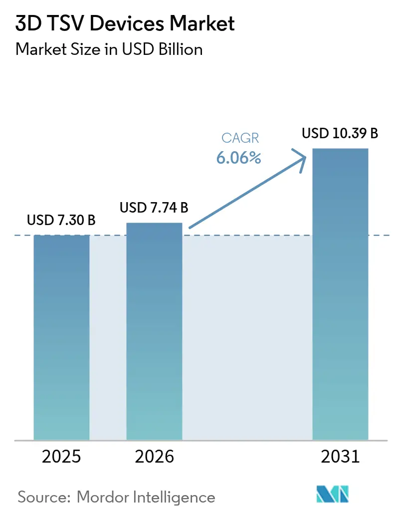
3D TSV Devices market size in 2026 is estimated at USD 7.74 billion, growing from 2025 value of USD 7.30 billion with 2031 projections showing USD 10.39 billion, growing at 6.06% CAGR over 2026-2031. Sustained demand from high-performance computing, AI accelerators, and advanced driver-assistance systems keeps capacity fully loaded, while government subsidies in the United States, Europe, and South Korea accelerate fab expansions. Logic–memory co-packaging, hybrid bonding, and chiplet-ready interposer designs are eliminating bandwidth bottlenecks and reducing TSV pitch to below 20 microns. Tool orders for deep reactive ion etch and copper fill remain elevated despite tighter environmental rules on fluorinated chemistries. Competitive intensity is rising as outsourced assembly and test (OSAT) houses race integrated device manufacturers (IDMs) to secure long-term contracts with hyperscalers and tier-one automotive suppliers. Small but rapidly growing white-space segments, such as silicon photonics co-packaging and implantable medical sensors, provide additional headroom for value creation.
Key Report Takeaways
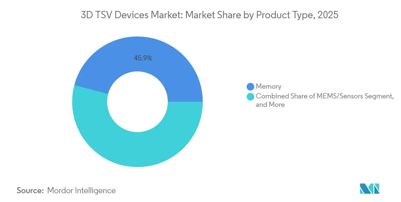
- By product type, memory led the 3D TSV devices market with a 45.92% market share in 2025; MEMS and sensors are expected to advance at a 8.57% CAGR through 2031.
- By TSV technology, via-middle contributed 54.15% of revenue of the 3D TSV devices market in 2025, while via-first is projected to expand at 7.69% CAGR to 2031.
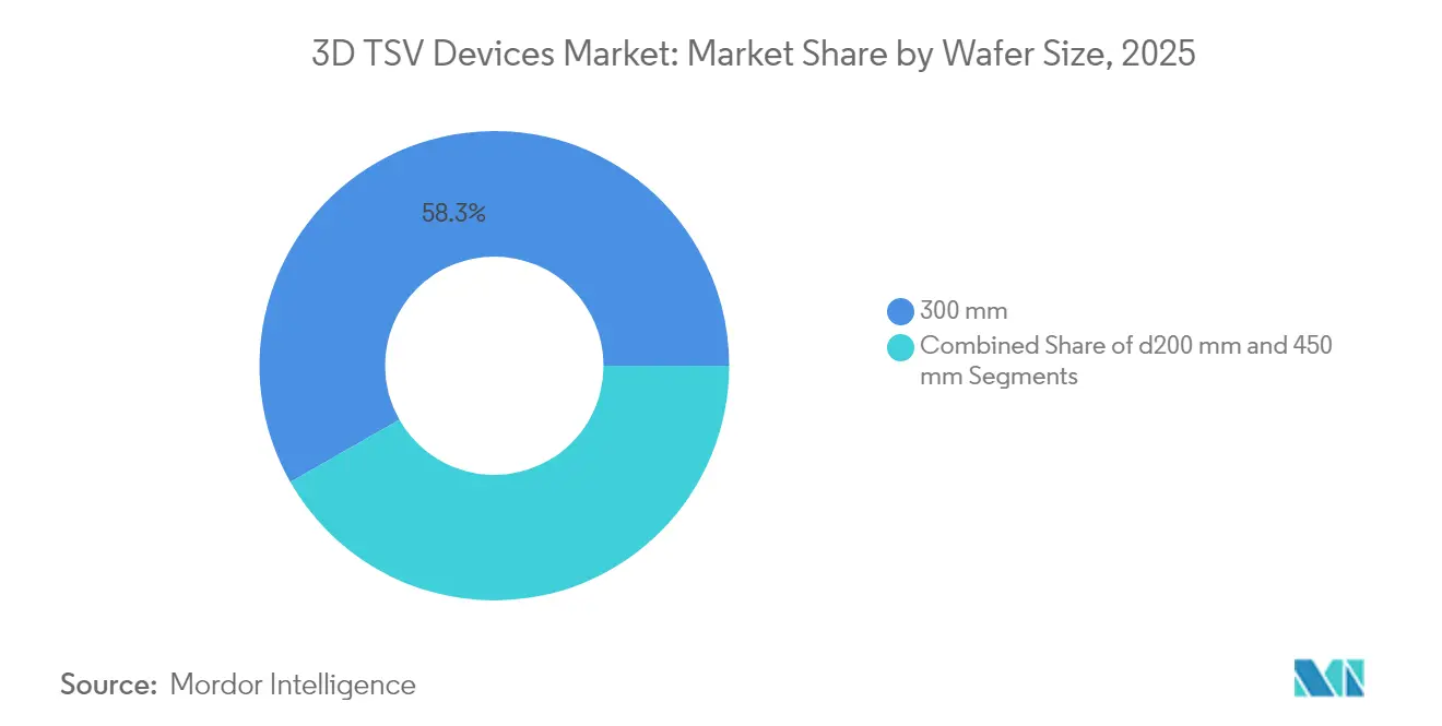
- By wafer size, 300 mm substrates accounted for 58.25% of the 3D TSV devices market size in 2025; the 450 mm segment is growing at an 7.88% CAGR.
- By end-user, IT and telecommunications accounted for 37.54% of the 3D TSV devices market in 2025, whereas the automotive segment is the fastest-growing, with a 9.08% CAGR.
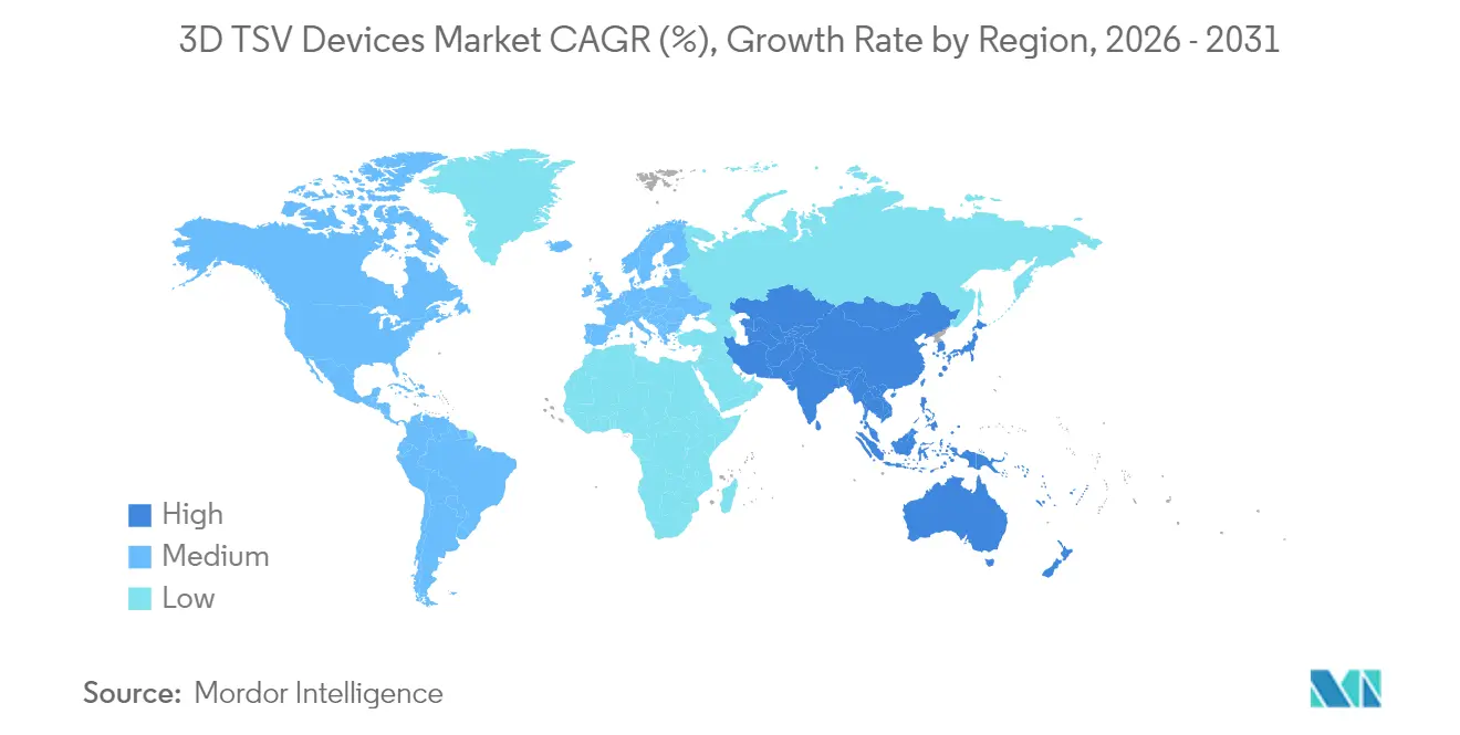
- By geography, the Asia-Pacific dominated the 3D TSV devices market, accounting for 42.70% of global revenue in 2025 and growing at an 8.56% CAGR to 2031. North America followed, boosted by USD 6.165 billion in CHIPS Act funding, which is expected to drive TSV packaging onshore.
Note: Market size and forecast figures in this report are generated using Mordor Intelligence’s proprietary estimation framework, updated with the latest available data and insights as of 2026.
Market Trends and Insights
Drivers Impact Analysis of 3D TSV Devices Market*
| Driver | (~) % Impact on CAGR Forecast | Geographic Relevance | Impact Timeline |
|---|---|---|---|
| Growing demand for high-performance computing and AI workloads | +1.8% | Global, with concentration in North America and Asia-Pacific | Medium term (2-4 years) |
| Expansion of data centers driving high-bandwidth memory adoption | +1.5% | Global, led by North America, Asia-Pacific, and Europe | Short term (≤ 2 years) |
| Rapid miniaturisation in smartphones and consumer electronics | +1.2% | Asia-Pacific core, with spill-over to North America and Europe | Medium term (2-4 years) |
| Chiplet-based heterogeneous integration architectures | +1.0% | Global, early adoption in North America and Asia-Pacific | Long term (≥ 4 years) |
| Silicon photonics' need for 3D interposer stacking | +0.4% | North America and Europe, with emerging activity in Asia-Pacific | Long term (≥ 4 years) |
| Government subsidies for advanced packaging fabs | +0.9% | North America, Europe, and select Asia-Pacific markets | Short term (≤ 2 years) |
| Source: Mordor Intelligence | |||
Growing Demand for High-Performance Computing and AI Workloads
Large language model training now exceeds 1 trillion parameters, forcing memory hierarchies to move beyond GDDR6. SK Hynix’s engineering samples of 12-high HBM4 stacks deliver a 2.1 Tbit/s bandwidth, a 64% increase over HBM3E, providing GPU clusters with headroom for matrix-multiply peaks.[1] JEDEC’s HBM4 standard, ratified in 2024, locks in a 2048-bit interface that only through-silicon via architectures can serve. Micron’s FY 2024 report indicates HBM revenue more than doubled, with USD 1.5 billion set aside for capacity that ramps in 2026.[2] Samsung’s shift to copper-to-copper hybrid bonding trims via resistance by 40%, improving multi-GHz signal integrity. Intel’s Gaudi 3 accelerator integrates eight HBM3E stacks on a silicon interposer, prompting a USD 3.5 billion packaging build-out in Arizona and New Mexico under CHIPS Act co-funding.
Expansion of Data Centers Driving High-Bandwidth Memory Adoption
Hyperscalers are deploying AI servers at record velocity, with NVIDIA H200 and AMD MI300X sockets each consuming over 80 GB of HBM3. TSMC’s CoWoS lines ran above 100% utilization throughout 2024, triggering a USD 2.8 billion expansion to 60k wafers/month in Taiwan. Micron’s May 2024 investor deck indicated that HBM supply was fully booked until 2025, potentially inflating average selling prices by 30%. Broadcom shipped custom AI ASICs that each integrate TSV-based HBM and deliver more than 3 Tbit/s bandwidth per package. These dynamics reinforce the near-term pricing power of the 3D TSV devices market.
Rapid Miniaturization in Smartphones and Consumer Electronics
Premium smartphones now target sub-8 mm thickness. Sony’s stacked CMOS image sensors, which account for over 50% of flagship camera modules shipped in 2024, utilize via-last TSV to attach logic without sacrificing pixel area, thereby boosting low-light sensitivity by 40%. Apple’s A18 Pro utilizes InFO-PoP with via-first TSV to reduce the z-height by 0.4 mm, thereby freeing up volume for a larger battery. Qualcomm’s Snapdragon 8 Gen 4 pairs its 3nm application processor with LPDDR5T via micro-TSVs, sustaining data rates of up to 9.6 GT/s for on-device generative AI. Wearables mirror this trend: TDK InvenSense’s IIM-20670 IMU stacks two dies with TSVs to fit inside 5 mm earbuds.
Chiplet-Based Heterogeneous Integration Architectures
As logic nodes approach their scaling limits, disaggregation enables each tile to utilize its optimal process. AMD’s Zen 5 CPUs utilize 3D V-Cache, stacked via-middle TSV, which reduces latency by 15 ns and boosts gaming frame rates by 25%. Intel’s Meteor Lake utilizes a Foveros base die with a 36 µm TSV pitch, enabling 2 Tbit/s data transfer among compute, graphics, and I/O tiles. The UCIe 1.1 specification, published in 2024, standardizes die-to-die links that rely on sub-100 pJ/bit TSV interconnects. Broadcom’s Tomahawk 5 Ethernet switch features 51.2 Tbit/s SerDes tiles surrounding a packet processor on a TSV-enabled interposer, illustrating how the 3D TSV devices market is inextricably linked to the chiplet era.
Restraints Impact Analysis of 3D TSV Devices Market*
| Restraint | (~) % Impact on CAGR Forecast | Geographic Relevance | Impact Timeline |
|---|---|---|---|
| High unit cost of 3D TSV packages | -1.2% | Global, with acute pressure in cost-sensitive consumer segments | Medium term (2-4 years) |
| Thermal-induced reliability and yield challenges | -0.9% | Global, particularly in high-layer-count HBM and logic stacks | Short term (≤ 2 years) |
| Supply-chain bottlenecks for TSV etch and fill tools | -0.5% | Asia-Pacific and North America, with secondary effects in Europe | Short term (≤ 2 years) |
| Stricter environmental rules on TSV chemistries | -0.3% | Europe and North America, with gradual adoption in Asia-Pacific | Long term (≥ 4 years) |
| Source: Mordor Intelligence | |||
High Unit Cost of 3D TSV Packages
A TSV assembly adds USD 15-40 to each device, thereby squeezing margins for mid-tier phones and IoT devices. Etch tools exceed USD 15 million per chamber, while electroplating systems cost another USD 8 million.[3] Amkor’s FY 2024 filings reveal advanced-packaging gross margins at 28%, or 500 bps below wire-bond levels. Qualification cycles are long; ASE’s Kaohsiung expansion highlighted that automotive-grade TSV packages require 1,000-hour HTOL testing, which can stretch the time-to-market by up to 16 weeks.
Thermal-Induced Reliability and Yield Challenges
HBM4 stacks dissipate more than 15 W over a 5 × 7 mm footprint, causing 80 µm warpage at 85 °C, per SK Hynix data presented at IEEE ECTC. Samsung’s hybrid-bond pilots achieved a 75% yield, constrained by copper planarity specifications of under 2 nm RMS. Intel’s Foveros Direct reported 82% known-good-die yield with void formation as the dominant defect. Micron’s sustainability report indicates that TSV-based DRAM requires 60% longer test times, resulting in an additional USD 3 per unit. TSMC’s qualification of diamond-like carbon heat spreaders improved hotspot mitigation by 30% but complicates material flows.
*Our forecasts treat driver/restraint impacts as directional, not additive. The impact forecasts reflect baseline growth, mix effects, and variable interactions.
3D TSV Devices Market Segment Analysis
By Product Type:
Memory Dominance Anchors Revenue BaseMemory devices captured 45.92% of the 3D TSV devices market in 2025 as HBM became the de facto high-bandwidth solution for AI accelerators. The 3D TSV devices market size for MEMS and sensors is projected to expand at an 8.57% CAGR to 2031, reflecting the adoption of automotive radar and inertial units. Imaging and optoelectronics benefit from via-last TSV, enabling Sony’s back-illuminated sensors that reach 90% quantum efficiency in near-IR. LED suppliers are using via-first TSV to power micro-LED displays, although yields below 60% delay mass deployment.
Other products, such as power management ICs and RF front-ends, utilize TSV to minimize inductance. Qualcomm’s QTM565 mmWave module hits 10 Gb/s in 1 cm³ packages, while Bosch’s BMA580 accelerometer stacks MEMS and ASIC dies for 1 µA standby current. These examples demonstrate how the 3D TSV devices industry expands beyond memory, even as HBM establishes the revenue floor.

By TSV Technology:
Via-First Gains Traction in Chiplet DesignsVia-middle held 54.15% of the revenue in 2025, due to the maturity of DRAM and CIS; however, via-first is growing at a 7.69% CAGR, as chiplet-based dies demand sub-1 µm overlay accuracy. Intel’s Foveros line hits 36 µm pitch today and targets 10 µm by 2026, unlocking >1 Tbit/s/mm² vertical bandwidth.
Via-last remains critical for sensors, keeping pixel fill factors above 95%. Hybrid bonding across all three approaches doubles interconnect density and will dominate after 2026, cementing TSV’s role as the backbone of the 3D TSV devices market.
By Wafer Size:
300 mm Substrates Anchor Volume ProductionWafers at 300 mm represented 58.25% of volume in 2025, supported by over 120 qualified fabs worldwide. The 3D TSV devices market size for 450 mm remains small but is growing at an 7.88% CAGR as TSMC and Samsung validate their pilot lines.
Intel redirected its 450 mm budget to advanced packaging, confirming industry consensus that TSV plus chiplets yield better ROIC. Sub-200 mm lines linger for GaN and SiC power devices, where TSV enables vertical conduction.
By End-User Industry:
Automotive Segment Accelerates FastestIT and telecom retained a 37.54% share in 2025, while automotive climbed fastest at a 9.08% CAGR, driven by EV domain controllers that integrate ADAS, infotainment, and battery management.
Consumer electronics sustain demand for stacked CIS and LPDDR, while healthcare pursues TSV-enabled implants under FDA-approved paths. Aerospace and defense rely on radiation-hardened TSV memory for a total dose tolerance of over 100 krad. Together, these verticals diversify revenue streams across the 3D TSV devices market.
Geography Analysis
APAC 3D TSV Devices Market
Asia-Pacific held 42.70% of revenue in 2025 and is expanding at 8.56% CAGR, fueled by TSMC’s >70% share of CoWoS capacity, Samsung’s 45% grip on HBM, and SK Hynix’s end-to-end integration in Icheon. Japan’s JPY 920 billion subsidy brings advanced packaging to Kumamoto by 2026, serving Sony and Denso. China’s YMTC eyes TSV for 3D NAND controller stacking, but export curbs slow scaling. South Korea’s KRW 26 trillion tax incentives underwrite 50 new TSV etch chambers at SK Hynix. India attracts USD 2.75 billion from Micron for a Gujarat OSAT facility starting 2026, sealing Asia’s position as the epicenter of the 3D TSV devices market.
North America 3D TSV Devices Market
North America captured roughly 34.40% in 2025. Micron won USD 6.165 billion to build HBM fabs in New York and Idaho under the CHIPS Act. Amkor’s USD 2 billion Arizona plant is scheduled to open in 2027, processing 300 mm TSV packages for the automotive and defense industries. Intel’s New Mexico and Arizona expansions triple Foveros capacity by 2026, while Canada invests CAD 240 million in Ottawa’s co-packaged optics pilot line. Near-shoring prompts Texas Instruments and NXP to relocate fan-out assembly to Mexico, although TSV tools remain scarce in the region.
EMEA and South America 3D TSV Devices Market
Europe owned about 18.55% in 2025. STMicroelectronics secured EUR 2.9 billion to scale 300 mm TSV lines in France. Infineon qualified via-middle TSV for GaN power devices in Dresden, cutting on-resistance by 35%. Fraunhofer IZM has achieved a pitch of 0 µm via pibrid bonding pion lots, and the U.K. invested GBP 50 million in a GaN TSV line for high-temperature EV inverters. South America and MEA together account for 4.35%, though Brazil and the UAE signal post-2027 capacity adds.
Regulatory Landscape
Export control and trade policy are increasingly material to 3D TSV devices, especially where TSV density and performance track advanced computing use cases. The US Department of Commerce, Bureau of Industry and Security (BIS) applies enhanced due-diligence measures for advanced computing integrated circuits (Federal Register action dated January 16, 2025). Advanced DRAM with high TSV counts can also fall under advanced-node control frameworks, which affects both IDMs and OSATs that assemble HBM and TSV interposer packages. Beyond licensing exposure, supply-chain documentation and customer or end-use screening requirements are rising for global shipments of TSV-based AI and HPC packages.
In Europe, the EU Chips Act framework (Regulation (EU) 2023/1781) is the regulatory anchor. It strengthens coordination for semiconductor crises and gives the European Commission mechanisms to request supply-chain information from undertakings, intersecting with TSV packaging visibility and reporting in constrained-capacity environments. On the environmental side, tighter controls on process chemistries (including fluorinated chemistries used in etch and cleans) continue to influence tool selection, abatement investment, and process qualification timelines for deep reactive ion etch and copper-fill related steps used in TSV manufacturing.
Value Chain Analysis
The 3D TSV devices value chain starts with upstream materials and equipment, moves through wafer processing and TSV formation, and ends in advanced packaging assembly and test. Key upstream inputs include silicon wafers (300 mm as the volume anchor), dielectric and barrier or seed materials for via liners and metallization, and high-capex equipment covering deep silicon etch, deposition, and copper electroplating. Equipment concentration and long tool lead times (reported at 12 to 18 months for specialized machinery used in advanced packaging and 3D stacking) translate into capacity gating at the packaging step rather than at front-end wafer starts.
Midstream, foundries and IDMs (notably TSMC, Samsung, and Intel) handle TSV-first and via-middle process integration for leading AI and HPC packages, while OSATs such as ASE and Amkor provide assembly, bumping, and test capacity, particularly for flows that use TSV-last reveal and high-volume manufacturing discipline. Downstream demand comes from hyperscalers, GPU and networking ASIC designers, and tier-one automotive suppliers that increasingly seek long-term packaging capacity. Integration and standards initiatives such as TSMC 3DFabric and UCIe reduce design friction for chiplet and interposer-based systems, but they also raise the bar for coordinated qualification across wafers, interposers and substrates, assembly, and reliability testing.
Competitive Landscape
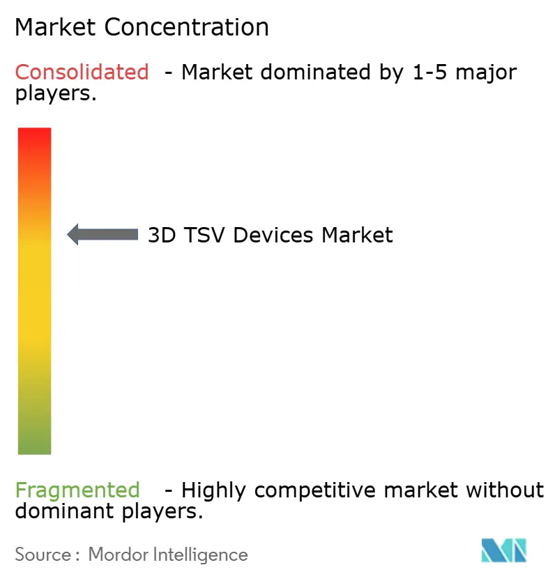
Market concentration is moderate to high, with the top five players accounting for roughly 75% of the value. TSMC alone garners more than 70% of advanced packaging for high-performance computing, securing wins from NVIDIA, AMD, and Broadcom. Samsung and SK Hynix collectively supply 85% of HBM, leveraging vertical stacks to lock customers into multi-year deals. Micron is closing the gap via the CHIPS Act–funded capacity for 2027.
OSAT majors ASE, Amkor, and JCET expand 300mm fan-out and TSV lines to attract fabless chiplet designers. ASE’s ISO 26262-certified Kaohsiung campus now supports automotive AI SoCs. Amkor broke ground on a trusted-supply facility in Arizona to serve defense contracts. JCET and Siliconware Precision Industries push adaptive patterning to cut micro-bump cost.
White-space opportunities emerge in silicon photonics co-packaging; Cisco and Intel need TSV interposers for 1.6 Tb/s Ethernet, a gap that Broadcom’s Tomahawk 5 already exploits. Start-ups such as Adeia license direct bond interconnect IP to Samsung and TSMC, dropping via pitch to 10 µm. Capital intensity and TSV chemistry patents still pose entry barriers, preserving incumbents’ pricing power across the 3D TSV devices market.
3D TSV Devices Industry Leaders
-
Taiwan Semiconductor Manufacturing Company Limited
-
Samsung Electronics Co., Ltd.
-
Intel Corporation
-
Micron Technology, Inc.
-
SK hynix Inc.
- *Disclaimer: Major Players sorted in no particular order
3D TSV Devices Market Companies Covered in this Report
- Taiwan Semiconductor Manufacturing Company Limited
- Samsung Electronics Co., Ltd.
- Intel Corporation
- Micron Technology, Inc.
- SK hynix Inc.
- Toshiba Electronic Devices and Storage Corporation
- ASE Technology Holding Co., Ltd.
- Amkor Technology, Inc.
- United Microelectronics Corporation
- STMicroelectronics N.V.
- Broadcom Inc.
- Texas Instruments Incorporated
- GlobalFoundries Inc.
- Advanced Micro Devices, Inc.
- Qualcomm Incorporated
- JCET Group Co., Ltd.
- Powertech Technology Inc.
- Siliconware Precision Industries Co., Ltd.
- Xilinx, Inc. (AMD Adaptive and Embedded Computing Group)
- Pure Storage, Inc.
Market Opportunities and Future Outlook
A primary opportunity is expanding qualified advanced-packaging capacity and broadening the supplier base for TSV-enabled interposers and stacks, since CoWoS-class capacity has operated at very high utilization. That has driven both in-house expansion and measured outsourcing to OSAT partners, leaving room for OSATs and substrate or interposer ecosystem players that can meet AI and HPC electrical and thermal requirements while following automotive-grade reliability pathways. (This includes the long HTOL qualification cycles referenced in automotive packaging ramps.)
The market also benefits from technology roadmaps that raise interconnect density. TSMC has outlined SoIC pitch scaling from a 6-micron class (2025) toward 4.5-micron by 2029, which supports higher bandwidth per package and tighter chiplet partitioning. A second opportunity area is tool and process innovation that reduces yield-ramp friction in TSV etch, metallization, bonding, and test. Packaging equipment lead times and yield learning function as choke points for HBM and TSV-heavy designs, encouraging investments in process control, metrology, and alternative integration approaches (including Intel EMIB-T bridge concepts) that can relieve bottlenecks without sacrificing bandwidth. Beyond AI and HPC, additional whitespace comes from silicon photonics co-packaging and compact sensor systems where TSV supports z-height reduction and high-density vertical interconnects, aligning with the report scope around logic-memory co-packaging, hybrid bonding, and chiplet-ready interposer designs that remove bandwidth constraints while tightening TSV pitch below 20 microns.
Recent Industry Developments in 3D TSV Devices Market
- June 2026: AT&S announced an expansion of its Kulim manufacturing site, including fit-out of Plant 2 and construction tied to IC substrate cores and advanced PCB capabilities. The expansion supports long-term demand from strategic technology partners, including AMD, and strengthens an enabling layer in the advanced packaging supply chain that complements TSV-based 2.5D/3D integration.
- April 2025: SK hynix unveiled 12-high HBM4 samples that exceed 2 Tbit/s bandwidth and confirmed a late-2026 mass production timing. This reinforces the role of high-density TSV stacking as a gating technology for AI accelerators and sustains demand for TSV etch, fill, bonding, and test capacity.
- December 2024: TSMC announced a USD 2.8 billion CoWoS expansion to reach 60k wafers per month by late 2025. The capacity step-up addresses advanced packaging constraints for TSV-enabled HBM and interposer-based AI compute, shaping allocation dynamics across foundries and OSAT partners.
3D TSV Devices Market Report Scope and Research Methodology
Market Definition and Coverage
For this study, the market covers revenues generated from 3D through-silicon via (TSV) based devices used to create vertical electrical connections for stacked dies in semiconductor components across key end-use industries.
Scope exclusions: We exclude non-TSV 3D packaging approaches and standard 2D packaging where vertical interconnects through silicon are not used.
Segments Covered in This Report
- By Product Type
- Imaging and Opto-Electronics
- Memory
- MEMS / Sensors
- LED
- Other Products
- By TSV Technology
- Via-Middle TSV
- Via-Last TSV
- Via-First TSV
- By Wafer Size
- ≤200mm
- 300 mm
- 450 mm
- By End-User Industry
- Consumer Electronics
- Automotive
- IT and Telecom
- Healthcare
- Aerospace and Defence
- Other End-User Industries
- By Geography
- North America
- United States
- Canada
- Mexico
- South America
- Brazil
- Argentina
- Rest of South America
- Europe
- Germany
- United Kingdom
- France
- Italy
- Spain
- Russia
- Rest of Europe
- Asia-Pacific
- China
- Japan
- India
- South Korea
- Australia
- Rest of Asia-Pacific
- Middle East and Africa
- Middle East
- Saudi Arabia
- United Arab Emirates
- Turkey
- Rest of Middle East
- Africa
- South Africa
- Nigeria
- Egypt
- Rest of Africa
- Middle East
- North America
Data Sources, Market Sizing, and Validation
Desk Research
Desk research was used to set the market boundary and to pick practical indicators that can be refreshed each year without relying on private datasets. We reviewed public materials such as semiconductor trade statistics, customs and export-import summaries, and macro indicators that help explain electronics demand by region.
To shape assumptions, we also referred to sources such as US SEC filings and annual reports, investor presentations, reputable business press, and technical papers in peer-reviewed journals that discuss TSV process flows (via-first, via-middle, via-last) and wafer trends. For quant checks, we used paid subscriptions for company financials and intelligence, patent databases, and a semiconductors value chain database to confirm capacity expansion signals and technology adoption timing. These examples are illustrative only, and many other public and paid sources were used to collect, validate, and clarify data points throughout the work.
Primary Interviews and Surveys
Primary work focused on interviews and structured surveys with executives, business unit leaders, and managers across the 3D TSV value chain, including manufacturing, packaging services, and end-market demand planning. Since this is a global market, inputs were checked across APAC, EMEA, and the Americas so we could validate adoption levels, typical pricing movement, and the timing of new capacity coming online.
Distribution of primary research fieldwork respondents
| Company type | Respondent position | Region |
|---|---|---|
| Top tier: 30% | CXOs: 13% | APAC: 48% |
| Mid tier: 56% | Functional/Unit leaders: 28% | EMEA: 30% |
| Smaller Players: 14% | Managers: 59% | Americas: 22% |
Market-Sizing & Forecasting
Sizing starts from a top-down reconstruction where semiconductor packaging demand and 3D integration adoption are translated into a 3D TSV device demand pool, and then allocated by product use and region. To keep the math grounded, we corroborate totals with selective bottom-up approximations, such as sampled shipment volumes multiplied by realistic ASP bands and cross-checked with supplier revenue cues where disclosure exists.
Inputs were tied to market fingerprints that respondents could sanity-check quickly, which is important when data is fragmented. Key variables used include: mix shift toward memory stacks and imaging and opto-electronics, TSV technology split (via-first, via-middle, via-last) as it affects yield and cost, wafer size progression (200 mm to 300 mm and beyond) that influences throughput, end-use demand signals from consumer electronics and automotive electronics, and regional capacity additions that change supply availability. When a bottom-up gap appeared, it was handled by using conservative penetration rates and then rechecking the implied volumes against the technology mix discussed in interviews.
For forecasting, scenario analysis was used so adoption and pricing could be adjusted under different outcomes for advanced packaging demand, capacity ramp success, and macro cycles. Assumptions for the main case were aligned to the most repeated expert views, and then the resulting growth path was tested for consistency with the key end-use demand drivers.
Data Validation & Update Cycle
Validation is done through triangulation across independent signals, and then through step-by-step review checks before a final sign-off. We compare the modeled market totals against regional demand cues, technology adoption commentary, and revenue patterns implied by public disclosures, and then we rework any outliers that do not match the logic of wafer size mix, end-use demand, or expected pricing movement.
If a major variance is found, follow-up calls are triggered to confirm whether it is a timing issue (for example, a delayed capacity ramp) or a scope mismatch. Reports are refreshed annually, and interim updates are made when material events occur, such as new fabrication lines, shifts in trade conditions, or a clear change in adoption pace. Before delivery, the latest market signals are reviewed again so the final view is current.
Mordor Intelligence's 3d Tsv Devices Market Size Versus Other Published Estimates
Published market sizes for 3D TSV devices can differ even when the topic name looks the same, because each publisher draws the boundary around products and packaging types differently and then applies different pricing and adoption assumptions. Timing also matters, since base years, currency conversions, and refresh cadence can shift the reported value.
Key gap drivers in this market usually come from whether the estimate includes 2.5D packages alongside 3D TSV devices, how the study treats adjacent advanced packaging revenue versus device-level TSV-enabled components, and how quickly ASP changes are assumed as wafer sizes and yields improve. Another common source of spread is how aggressively the model assumes demand from memory stacks, imaging, and automotive electronics ramps, especially when capacity expansions are announced but not yet fully utilized.
Benchmark comparison
| Source | Market Size | Gaps in Research Methodology |
|---|---|---|
| Mordor Intelligence | USD 7.74 B (2026) | |
| Industry Research House A | USD 8.93 B (2025) | Uses an earlier base year and applies adoption and pricing assumptions that appear to pull more value from imaging, opto-electronics, and memory use cases into the starting point, which can lift the near-term total versus a 2026 anchor. |
| Global Consultancy B | USD 1.10 B (2024) | Frames the market around a narrower definition that blends type labels (including 2.5D packages) and can undercount device-level TSV enablement across end-user industries, which compresses the stated value for the base year. |
By tracking TSV technology splits, wafer size mix, and end-use adoption signals, Mordor Intelligence keeps the estimate tied to device-level TSV enablement and avoids pulling in adjacent packaging revenue that is not consistently reported. Taken together, the table suggests the spread is mainly driven by scope boundaries, base-year choice, and how ASP and adoption are refreshed, which is why a transparent set of inputs makes the number easier to reproduce and update.
Key Questions Answered in the Report
How fast is global demand for high-bandwidth memory growing?
HBM revenue doubled in 2024 and is driving a 6.06% CAGR for the overall 3D TSV market through 2031.
Which TSV technology is gaining the most traction in chiplet designs?
Via-first TSV is forecast to expand 7.69% CAGR as base dies demand sub-1 µm overlay accuracy.
Why is automotive considered the fastest-growing vertical?
Electric-vehicle domain controllers need stacked sensor-fusion processors, pushing automotive TSV demand at 9.08% CAGR.
What role do government incentives play in capacity expansion?
CHIPS Act awards in the U.S. and similar programs in Europe and Asia underwrite multi-billion-dollar TSV fabs, accelerating on-shore supply.
How concentrated is supplier power in advanced packaging?
Five players control roughly 75% of revenue, giving the sector a concentration score of 7 on a 10-point scale.
When will 450 mm TSV production reach meaningful scale?
Pilot lines exist today, but mainstream 450 mm adoption is unlikely before 2028 as tooling ecosystems mature.