3D TSV And 2.5D Market Size and Share
3D TSV And 2.5D Market Analysis by Mordor Intelligence
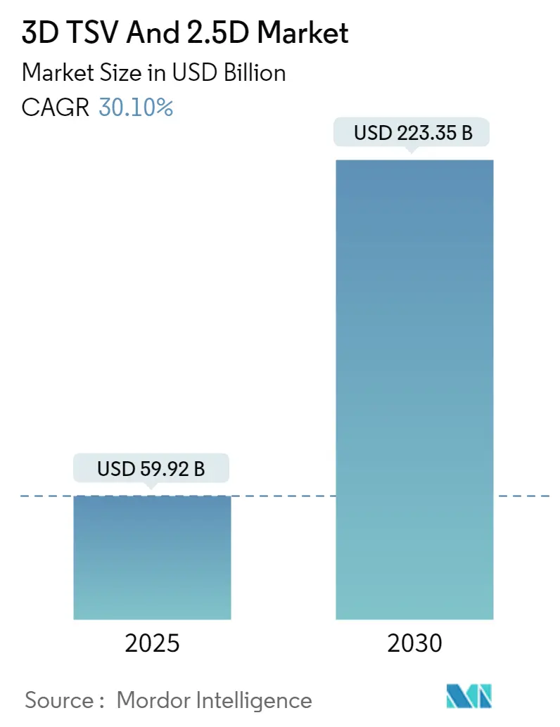
The 3D TSV And 2.5D Market size is estimated at USD 59.92 billion in 2025, and is expected to reach USD 223.35 billion by 2030, at a CAGR of 30.1% during the forecast period (2025-2030).
Packaging in the semiconductor industry has noticed a continuous transformation. As the semiconductor applications are growing, the slowdown in CMOS scaling and escalating prices have forced the industry to rely on the advancement in IC packaging. 3D stacking technologies are the solution that meets the required performance of applications like AI, ML, and data centers. Therefore, the growing requirement for high-performance computing applications mainly drives the TSV (Through Silicon Via) market over the forecast period.
- The 3D TSV packaging technology is also achieving traction. It reduces data transmission time between chips and the current wire bonding technology, resulting in significantly lower power consumption with faster speed. In October 2022, TSMC announced the launch of the creative 3DFabric Alliance, a considerable introduction to TSMC's Open Innovation Platform (OIP) to help customers overcome the surging hurdles of semiconductor and system-level design challenges. It will also help in gaining rapid integration of advancements for next-generation HPC and mobile technologies using TSMC's 3DFabric technologies.
- Increasing consumer demand for electronics has sparked the need for advanced semiconductor devices that enable various new capabilities. As the demands for semiconductor appliances intensify consistently, advanced packaging techniques deliver the form factor and processing power required for today's digitized world. For instance, according to the Semiconductor Industry Association, during August 2022, global semiconductor industry sales were USD 47.4 billion, a slight boost of 0.1% over the August 2021 total of USD 47.3 billion.
- In addition, according to the GSM Association, by 2025, the United States is expected to have the highest smartphone adoption globally (49% of connections). As per the United States IoT Association, it has the highest smart home device ratio per household and the most significant consumer tendency to own appliances across two or three use cases (energy, security, and appliances).
- Moreover, in September 2022, the Biden administration announced that it would invest USD 50 billion in building up the domestic semiconductor industry to counter dependency on China, as the US produces zero and consumes 25% of the world's leading-edge chips vital for its national security. President Joe Biden signed a USD 280 billion CHIPS bill in August 2022 to boost domestic high-tech manufacturing, part of his administration's push to increase US competitiveness over China. Such robust investments in the semiconductor sector would present lucrative opportunities for the growth of the studied market.
- The growth of MEMS and Sensors is attributed to the rapidly increasing demand for sensors and displays in various applications such as automotive, industrial automation, and many others. In August 2022, STMicroelectronics, a maker of MEMS and a significant player in the worldwide semiconductor industry, launched its third generation of MEMS sensors designed for consumer smart industries, mobile devices, healthcare, and retail sectors. The robust, chip-sized motion and environmental sensors power the user-friendly, context-aware features of today's smartphones, and wearables are made on MEMS technology. ST's most recent MEMS sensor generation drives technical boundaries regarding output accuracy and power consumption, elevating performance to a new level.
- Furthermore, the high costs associated with TSV device manufacturing restrict market growth. This includes not only the cost of devices but also the cost of accessories and consumables needed for their proper functioning. Moreover, the stringent guidelines and regulations governing TSV device manufacturing also add to the charges.
- Furthermore, the worldwide semiconductor shortage encouraged players to focus on expanding production capacity during a post-pandemic. For instance, the SMIC announced aggressive plans to double its production capacity by 2025 by constructing unique chip fabrication plants in different cities. Also, many Asian-Pacific local governments have funded the semiconductor industry in a long-term program, hence anticipated to regain market growth. For instance, the Chinese government introduced roughly USD 23-30 billion to pay for the second stage of its National IC Investment Fund 2030.
- Moreover, the ongoing conflict between Russia and Ukraine is expected to impact the electronics industry significantly. The conflict has already exacerbated the semiconductor supply chain issues and the chip shortage that have affected the industry for some time. The disruption may come in the form of volatile pricing for critical raw materials such as nickel, palladium, copper, titanium, aluminum, and iron ore, resulting in material shortages. This would obstruct the manufacturing of 3D Stacked Memory.
Global 3D TSV And 2.5D Market Trends and Insights
LED Packaging Expected to Witness the Significant Growth
- The increasing use of LED in products has promoted the expansion of higher power, greater density, and lower-cost devices. Using three-dimensional (3D) packaging through silicon via (TSV) technology authorizes a high density of vertical interconnects, unlike 2D packaging.
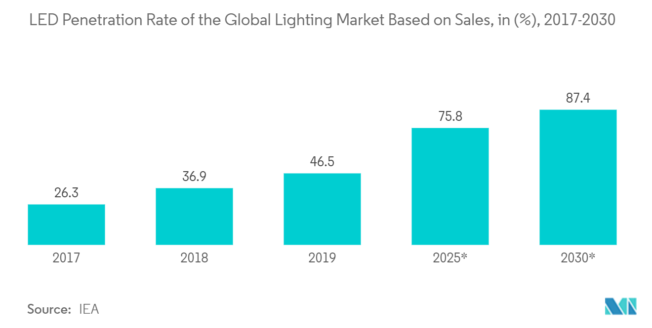
- TSV integrated circuits reduce connection lengths; thus, smaller parasitic capacitance, inductance, and resistance are required where a combination of monolithic and multifunctional integration is done efficiently, providing high-speed, low-power interconnects. According to IEA, the penetration rate of LEDs into the international lighting market is expected to reach some 76% in 2025 and further to 87.4% in 2030.
- Further, government initiatives and rules to adopt energy-efficient LEDs drive the studied Market. According to the International Energy Agency (IEA), the growth rate of LEDs in the lighting market is anticipated to be 75.8% in 2025.
- The requirements for LED packaging could be much better. If LED chips are not positioned into the package precisely, the luminescence efficiency of the overall packaging appliance might be affected directly. Any deviation from the established position will prevent LED light from being fully reflected from the reflective cup, affecting the LED's brightness.
- The US Department of Energy recently announced investing USD 61 million in 10 pilot projects using the latest technologies to turn thousands of homes and businesses into cutting-edge, energy-efficient networks. This applies to switching out incandescent and halogen bulbs for better energy-efficient LED lighting. As a result, with the expansion in LEDs, the LED packaging need in the United States will grow in the forecasted period.
- Furthermore, various players in the market are developing new products in the studied Market. In May 2022, Lumileds LLC launched high-power CSP (chip-scale package) LED. The LUXEON HL1Z is an un-domed, single-sided emitter that delivers high luminous efficacy (137lm/W or more) from a tiny box, just 1.4mm square.
- Rapid advancements in LED package applications are projected to raise innovation and consumption in the coming years, propelling the studied market growth. On the other hand, high saturation may limit product acceptance, which, in turn, limits market growth.
Asia-Pacific is Expected to Hold the Significant Market Share
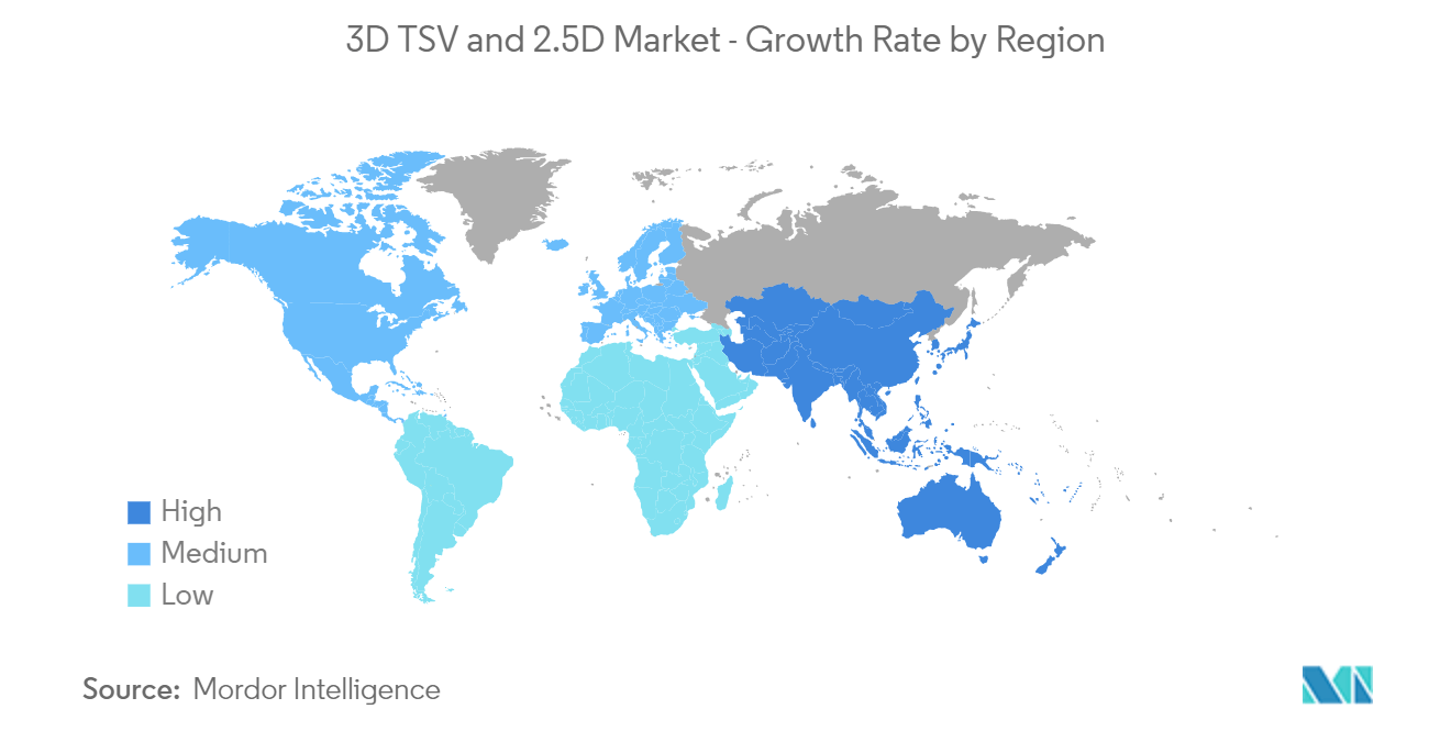
- Asia-Pacific is the significant-growing region in the Market studied. The rising smartphone adoption rates have made the region one of the major mobile markets in the world, primarily due to the increasing population evolution and urbanization.
- As per the GSM Association, smartphone broadband networks cover 96% of the population of APAC, with 1.2 billion people accessing mobile internet services. 5G momentum continues revving across the region, with commercial 5G services currently available across 14 markets. Several others, including India and Vietnam, are expected to board in the coming years. By 2025, there will be 400 million 5G connections across the region, over 14% of the population. Further, industry 4.0 is also one of Asia-Pacific's most emerging trends. IoT devices and miniaturization are important trends in Industry 4.0, utilizing 3D TSV. The region is investing heavily in IoT to support smart city infrastructure.
- Advancing technologies have contributed to the development of consumer electronics, telecom, medical devices, communication devices, and automotive. With the launch of 5G benefits in the country, the demand for smartphones, among other things, has been rising.
- According to the MIIT, China desired 2 million installed 5G base stations in 2022 to develop the country's next-generation mobile network. The Chinese mainland presently has 1.425 million installed 5G base stations that support more than 500 million 5G users nationally, making it the most comprehensive network in the world, as per MIIT. The growing implementation of 5G in the region is also expected to promote the demand for 5G-enabled devices, thereby increasing the need for 2.5D and 3D semiconductor packaging.
- Further, according to CAICT, 5G smartphone shipments are recorded for 75.9% of domestic shipments, more significant than a global average of 40.7%. By July 2022, 5G smartphones will have reached 74% of all cellphone shipments in China. The total number of 5G cell phone shipments by July 2022 was 124mm units, and China introduced 121 latest 5G mobile phone models. Such trends would accelerate the region's demand for 2.5D and 3D semiconductor packaging solutions.
- The increasing use of autonomous and electric vehicles has also increased the demand for advanced semiconductors across the region, further supporting the studied Market's growth. In February 2022, Tesla plans to build a 2nd EV facility in China to keep up with rising demand locally and in export markets. In the short term, Tesla intends to increase capacity in China to at least 1mm cars yearly, with a second plant planned around its present exhibition in Shanghai's Lingang free trade zone. In addition, the Chinese government seeks 20% of all vehicle sales to be electric by 2025, including adopting NEVs as the next generation of government vehicles.
- Moreover, the growing investments in semiconductor manufacturing and packaging plants also create a favorable growth scenario for the studied Market. For instance, Intel, a significant semiconductor chip manufacturer, recently announced a USD 7 billion investment to build an advanced chip packaging facility in Malaysia. Similarly, in November 2022, Advanced Semiconductor Engineering (ASE) announced a USD 300 million investment to expand its production site in Malaysia.
Competitive Landscape
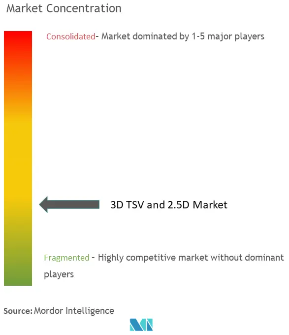
The 3D TSV and 2.5D market is highly competitive and consists of various significant performers as it is diversified. The existence of small, large, and local vendors in the Market creates excellent competition. These firms leverage strategic collaborative endeavors to expand their market share and increase profitability. The companies in the Market are also acquiring start-ups performing on enterprise network equipment technologies to strengthen their product capabilities.
In August 2022, Intel showcased the unique architectural and packaging breakthroughs that help 2.5D and 3D-based chip designs, ushering in a remarkable era in chipmaking technologies and their importance. Intel's system foundry model features enhanced packaging. The organization intends to improve the number of transistors on a package from 100 billion to 1 trillion by 2030.
In March 2022, Apple adopted a 2.5D approach to boost the enactment of its latest M1 Ultra device that unlocks the door to future designs utilizing chiplets. A packaging architecture called UltraFusion interconnects the die of two M1 Max chips on a silicon interposer to build a system on a chip (SoC) with 114bn transistors. This utilizes a silicon substrate and interposer that supports the two dies with 10,000 interconnects with 2.5 TB/s of low latency and inter-processor bandwidth between the die. This also connects the die to 128 GB of low-latency unified memory operating an 800 GB/s interface.
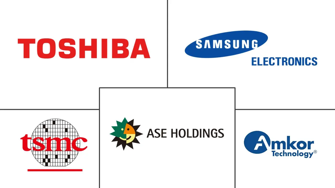
3D TSV And 2.5D Industry Leaders
-
Toshiba Corp.
-
Samsung Electronics Co. Ltd
-
ASE Group
-
Taiwan Semiconductor Manufacturing Company Limited
-
Amkor Technology, Inc.
- *Disclaimer: Major Players sorted in no particular order
Recent Industry Developments
- October 2022: TSMC launched its Open Innovation Platform 3DFabric Alliance at the 2022 Open Innovation Platform Ecosystem Forum. The latest TSMC 3DFabric Alliance would be TSMC's sixth OIP Alliance and the first of its kind in the semiconductor enterprise for collaborating with different partners to accelerate 3D IC ecosystem innovation with a full spectrum of solutions and services for semiconductor design, substrate technology, testing, packaging, memory modules, and manufacturing.
- September 2022: Siemens Digital Industries Applications designed an integrated tools flow for 2.D and 3D stacked chip layouts. The firm recently teamed with foundry UMC to fabricate these designs. Because most historical IC test methodologies are designed on traditional two-dimensional methods, 2.5D and 3D structures can create substantial hurdles for IC testing. Tessent Multi-die software collaborated with Siemens' Tessent TestKompress Streaming Scan Network technology and Tessent IJTAG applications to overcome these problems. These optimize DFT test capabilities for every block without regard for the overall design, speeding DFT implementation and preparing for the 2.5D and 3D IC generation.
- June 2022: ASE Group introduced VIPack, an advanced packaging platform that enabled vertically integrated packaging solutions. The VIPack represents ASE's next-generation 3D heterogeneous integration architecture that expands design rules and delivers ultra-high density and performance.
Global 3D TSV And 2.5D Market Report Scope
The TSV is a high-performance interconnect technique that passes through a silicon wafer by a vertical electrical relation, lowering power consumption and enhancing electrical performance.
The studied market is segmented by packaging type, 3D stacked memory, 2.5D interposer, CIS with TSV, and 3D SoC, among various End-user Applications such as consumer Electronics, automotive, high-performance computing (HPC), and networking in multiple geographies (North America, Europe, Asia-Pacific, and Rest of the World). The impact of macroeconomic trends on the market and influenced segments are also covered under the scope of the study. Further, the disturbance of the factors affecting the market's evolution in the near future has been covered in the study concerning drivers and restraints.
The market sizes and forecasts are provided in terms of value USD for all the above segments.
| 3D Stacked Memory |
| 2.5D Interposer |
| CIS with TSV |
| 3D SoC |
| Other Packaging Types ( LED, MEMS & Sensors, etc.) |
| Consumer Electronics |
| Automotive |
| High Performance Computing (HPC) and Networking |
| Other End User Applications |
| North America | U.S. |
| Canada | |
| Europe | United Kingdom |
| Germany | |
| France | |
| Italy | |
| Rest of Europe | |
| Asia-Pacific | China |
| India | |
| Japan | |
| Australia | |
| South East Asia | |
| Rest of Asia-Pacific | |
| Rest of the World |
| By Packaging Type | 3D Stacked Memory | |
| 2.5D Interposer | ||
| CIS with TSV | ||
| 3D SoC | ||
| Other Packaging Types ( LED, MEMS & Sensors, etc.) | ||
| By End User Application | Consumer Electronics | |
| Automotive | ||
| High Performance Computing (HPC) and Networking | ||
| Other End User Applications | ||
| By Geography | North America | U.S. |
| Canada | ||
| Europe | United Kingdom | |
| Germany | ||
| France | ||
| Italy | ||
| Rest of Europe | ||
| Asia-Pacific | China | |
| India | ||
| Japan | ||
| Australia | ||
| South East Asia | ||
| Rest of Asia-Pacific | ||
| Rest of the World | ||
Key Questions Answered in the Report
How big is the 3D TSV And 2.5D Market?
The 3D TSV And 2.5D Market size is expected to reach USD 59.92 billion in 2025 and grow at a CAGR of 30.10% to reach USD 223.35 billion by 2030.
What is the current 3D TSV And 2.5D Market size?
In 2025, the 3D TSV And 2.5D Market size is expected to reach USD 59.92 billion.
Who are the key players in 3D TSV And 2.5D Market?
Toshiba Corp., Samsung Electronics Co. Ltd, ASE Group, Taiwan Semiconductor Manufacturing Company Limited and Amkor Technology, Inc. are the major companies operating in the 3D TSV And 2.5D Market.
Which is the fastest growing region in 3D TSV And 2.5D Market?
Asia Pacific is estimated to grow at the highest CAGR over the forecast period (2025-2030).
Which region has the biggest share in 3D TSV And 2.5D Market?
In 2025, the North America accounts for the largest market share in 3D TSV And 2.5D Market.
What years does this 3D TSV And 2.5D Market cover, and what was the market size in 2024?
In 2024, the 3D TSV And 2.5D Market size was estimated at USD 41.88 billion. The report covers the 3D TSV And 2.5D Market historical market size for years: 2019, 2020, 2021, 2022, 2023 and 2024. The report also forecasts the 3D TSV And 2.5D Market size for years: 2025, 2026, 2027, 2028, 2029 and 2030.
Page last updated on:
3D TSV And 2.5D Market Report
Statistics for the 2025 3D TSV And 2.5D market share, size and revenue growth rate, created by Mordor Intelligence™ Industry Reports. 3D TSV And 2.5D analysis includes a market forecast outlook for 2025 to 2030 and historical overview. Get a sample of this industry analysis as a free report PDF download.
