3D Sensing And Imaging Market Size and Share
Market Overview
| Study Period | 2020 - 2031 |
|---|---|
| Market Size (2026) | USD 14.98 Billion |
| Market Size (2031) | USD 28.65 Billion |
| Growth Rate (2026 - 2031) | 13.84% CAGR |
| Fastest Growing Market | Asia-Pacific |
| Largest Market | North America |
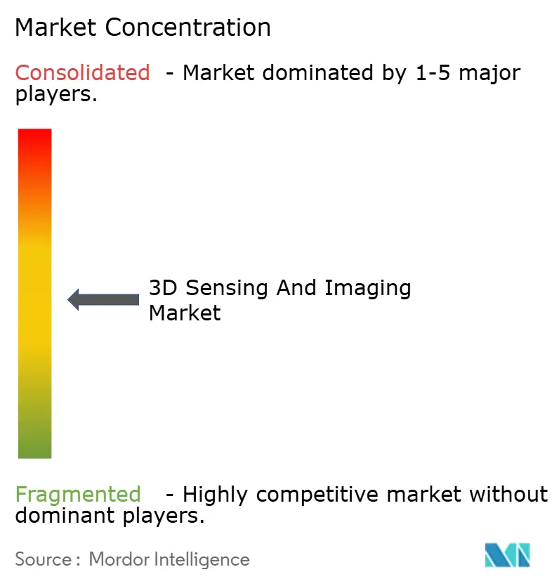
| Market Concentration | Medium |
Major Players *Disclaimer: Major Players sorted in no particular order Image © Mordor Intelligence. Reuse requires attribution under CC BY 4.0. | |
3D Sensing And Imaging Market Analysis by Mordor Intelligence
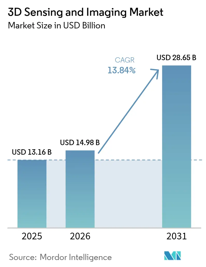
The 3D sensing and imaging market size is expected to grow from USD 13.16 billion in 2025 to USD 14.98 billion in 2026 and is forecast to reach USD 28.65 billion by 2031 at 13.84% CAGR over 2026-2031. Rapid integration of depth sensors in mid-tier smartphones, accelerating deployment of solid-state LiDAR in advanced driver assistance systems, and growing demand for real-time 3D medical imaging anchor this growth trajectory. Advancements in vertical-cavity surface-emitting laser (VCSEL) chiplets, coupled with lower-cost 3D semiconductor stacks, are eroding price barriers and expanding use cases across industrial inspection and climate analytics. Meanwhile, supply-chain exposure to gallium arsenide epi-wafer shortages and evolving biometric privacy regulations temper the near-term outlook but have not derailed investment programs by automotive, healthcare, and consumer-electronics OEMs seeking spatial intelligence at scale. Incumbent semiconductor vendors use portfolio breadth and wafer-level manufacturing control to retain leadership, yet specialized depth-sensing startups are closing the performance-per-dollar gap through AI-optimized algorithms and chiplet architectures.
Key Report Takeaways
- By component, hardware led with 72.15% of revenue of the 3D sensing and imaging market in 2025, while services are projected to advance at a 14.88% CAGR through 2031.
- By technology, time-of-flight accounted for 43.25% of the 2025 revenue of the 3D sensing and imaging market, whereas ultrasound-based sensing is set to grow at a 15.62% CAGR to 2031.
- By sensor type, image sensors captured 45.12% of 2025 sales of the 3D sensing and imaging market, and proximity sensors are forecast to expand at a 16.02% CAGR through 2031.
- By connectivity, wireless networks dominated with a 58.05% share of the 3D sensing and imaging market in 2025 and are also the fastest-growing at a 14.71% CAGR to 2031.
- By end-user industry, consumer electronics held 39.65% of the 2025 revenue of the 3D sensing and imaging market, while healthcare applications are rising at a 16.08% CAGR through 2031.
- By geography, North America led with 37.85% revenue of the 3D sensing and imaging market in 2025, but Asia-Pacific is projected to climb at a 15.74% CAGR to 2031.
Note: Market size and forecast figures in this report are generated using Mordor Intelligence’s proprietary estimation framework, updated with the latest available data and insights as of 2026.
Global 3D Sensing And Imaging Market Trends and Insights
Drivers Impact Analysis*
| Driver | (~) % Impact on CAGR Forecast | Geographic Relevance | Impact Timeline |
|---|---|---|---|
| Smartphone roll-out of structured-light depth cameras | +3.2% | Global; Asia-Pacific manufacturing hubs | Medium term (2-4 years) |
| Automotive ADAS adoption of solid-state LiDAR | +2.8% | North America, Europe, expanding Asia-Pacific | Long term (≥ 4 years) |
| Industry 4.0 3D machine-vision inspection | +2.1% | Global manufacturing centers | Medium term (2-4 years) |
| Healthcare demand for minimally invasive real-time 3D imaging | +1.9% | North America, Europe, emerging markets | Long term (≥ 4 years) |
| VCSEL-on-CMOS chiplets for sub-USD 1 sensors | +1.7% | Global; Asia-Pacific fabrication leadership | Short term (≤ 2 years) |
| Satellite 3D Earth-observation constellations | +1.5% | Global government and research agencies | Long term (≥ 4 years) |
| Source: Mordor Intelligence | |||


Widespread Smartphone Integration of Structured-Light 3D Cameras
Structured-light depth modules once reserved for premium flagships are now commonplace in mid-range handsets, lowering entry costs and normalizing user expectations for spatial photography, AR gaming, and secure face authentication. Apple’s iPhone 15 Pro LiDAR module validated consumer appetite for spatial computing, while Android OEMs rapidly released cost-reduced structured-light solutions. OmniVision’s April 2025 unveiling of a 1.5-megapixel global-shutter sensor for driver monitoring illustrates technology spillover from phones to vehicles, deepening economies of scale.[1]EEJournal Staff, “OMNIVISION Launches 1.5-Megapixel Global Shutter Sensor for Automotive Driver Monitoring Systems,” eejournal.com Volume ramp-ups push component pricing toward the sub-USD 1 threshold, unlocking adoption in industrial scanners and handheld medical devices.
Automotive ADAS Demand for Solid-State LiDAR Depth Maps
Vehicle makers are phasing out rotating LiDAR heads in favor of solid-state frequency-modulated continuous-wave (FMCW) units that offer vibration tolerance, velocity measurement, and lower cost. Daimler Truck’s 2024 selection of Aeva FMCW LiDAR underscored industry confidence in chip-scale depth sensors for Level 4 trucking fleets. Although automotive homologation extends timelines, Tier-1 suppliers with zero-defect manufacturing credentials stand to gain recurring design wins as ADAS moves down the vehicle price curve.
Industry 4.0 Adoption of 3D Machine-Vision Inspection Systems
Smart factories prioritize in-line 3D metrology to achieve zero-defect output in increasingly high-mix production. Keyence grew 2024 revenue to USD 7.061 billion with operating margins above 51.9%, attributable in part to instant measurement systems performing 99-dimensional checks in under three seconds.[2]Keyence Corporation, “Our Technology,” keyence.com These systems shave scrap rates and enable rapid line changeovers, ensuring robust demand for AI-assisted depth analysis software that accompanies hardware installs.
Healthcare Shift Toward Minimally Invasive, Real-Time 3D Imaging
Medical-device firms integrate micrometer-class 3D sensors into endoscopes, catheters, and navigation probes to enhance surgical precision and shorten recovery. OmniVision’s OH0TA sensor packs 400×400 RGB pixels at 30 fps inside a tip smaller than a grain of rice, running on just 20 mW. Surgeons gain depth perception that mitigates reliance on mental reconstruction from 2D images, supporting procedure time reductions and better outcomes that justify premium device pricing.
Restraints Impact Analysis*
| Restraint | (~) % Impact on CAGR Forecast | Geographic Relevance | Impact Timeline |
|---|---|---|---|
| Scarcity of high-power GaAs epi-wafers | -1.8% | Global; Asia-Pacific fabrication centers | Short term (≤ 2 years) |
| Calibration complexity in multi-sensor camera modules | -1.2% | Global manufacturing regions | Medium term (2-4 years) |
| Cyber-security risks from depth-map spoofing | -0.9% | North America, Europe | Medium term (2-4 years) |
| Uncertain rules on public-space biometric capture | -0.7% | Europe, North America, expanding worldwide | Long term (≥ 4 years) |
| Source: Mordor Intelligence | |||
Supply-Chain Scarcity of High-Power GaAs Epi-Wafers
Gallium arsenide substrate output remains concentrated among a handful of Asia-Pacific growers, creating price spikes and 20-week lead times for high-power VCSELs used in long-range time-of-flight modules. Sensor makers redesign optics for lower peak current draw and pursue silicon nitride photonics as a hedge, but near-term unit allocations still constrain automotive LiDAR rollout schedules.
Calibration Complexity Across Multi-Sensor Camera Modules
RGB, infrared, and depth elements stitched into single assemblies demand sub-pixel alignment over operating conditions from -40 °C to +85 °C. Automotive safety standards mandate 15-year stability, forcing vendors to adopt self-calibrating architectures and AI-based drift detection. Certification cycles lengthen, elevating engineering costs and raising the barrier to entry for new market entrants.
*Our forecasts treat driver/restraint impacts as directional, not additive. The impact forecasts reflect baseline growth, mix effects, and variable interactions.
Segment Analysis
By Component: Hardware Dominance Faces Services Disruption
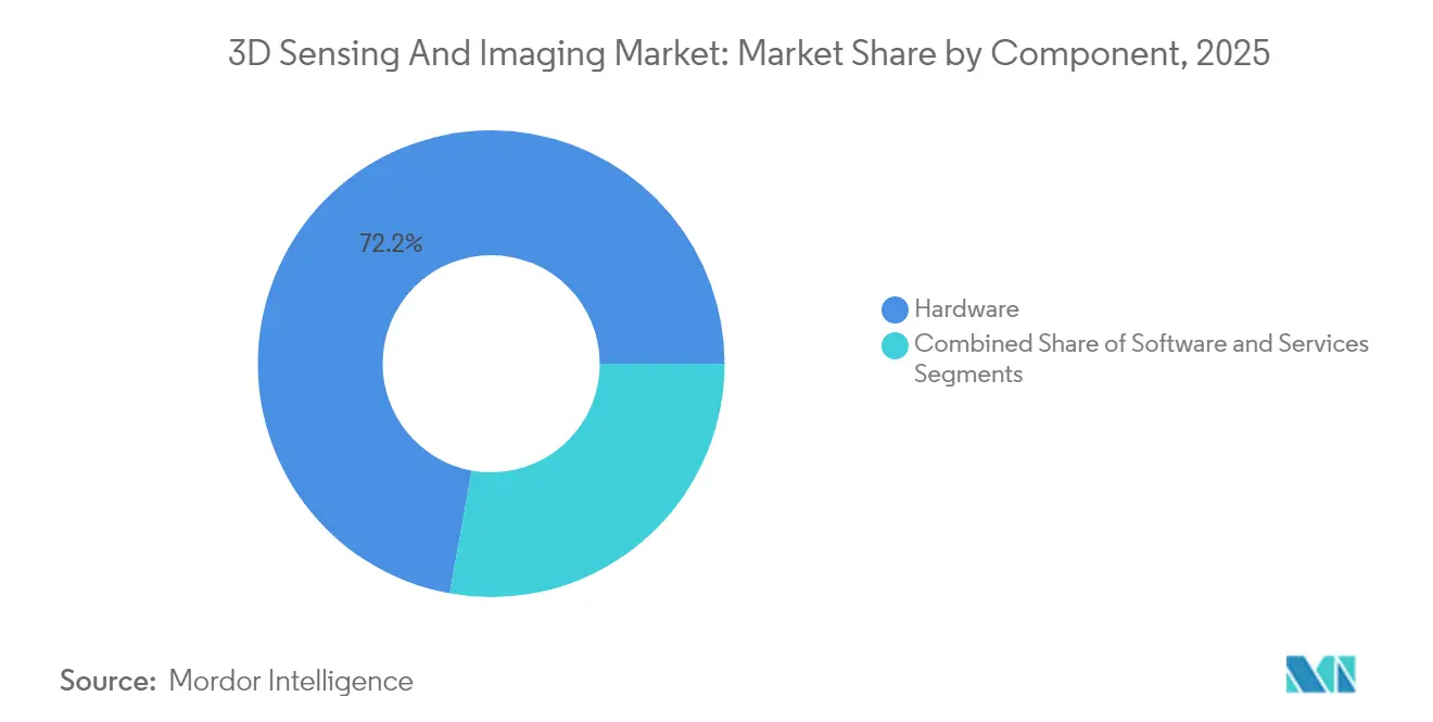
Hardware retained 72.15% of the 3D sensing and imaging market in 2025, yet services are growing 14.88% CAGR to 2031 as buyers seek turnkey deployments and outcome-based pricing. Faro Technologies now derives 20.9% of quarterly revenue from software and recurring cloud analytics, illustrating how calibration, maintenance, and AI model updates create annuity streams. Vendors package installation and lifetime support to secure multi-year deals, gradually tilting revenue mix toward services.
Demand for edge AI tool-chains that compress depth maps into actionable events further propels software attach rates. This erosion of pure-play hardware margins pressures component suppliers to form alliances with cloud and middleware providers, ensuring ecosystem stickiness and data-driven upsell potential.


By Technology: Time-of-Flight Leadership Challenged by Ultrasound Innovation
Time-of-flight kept a 43.25% share in 2025 because its silicon photodiodes and VCSEL drivers align with smartphone cost envelopes, securing billions of annual units. The 3D sensing and imaging market size for ultrasound-based systems, however, is projected to expand 15.62% annually as acoustic transducers excel in bright-sunlight and translucent-material scenarios. Industrial robotics adopts hybrid optical-ultrasound stacks for defect detection on glossy metals, while hospitals favor ultrasound depth probes for radiation-free fetal and cardiac imaging. Sensor designers leverage 3D-stacked CMOS to co-locate ultrasound receive circuits and optical imagers, yielding sensing clusters that toggle modality based on the environment.
By Sensor Type: Image Sensors Face Proximity Sensor Disruption
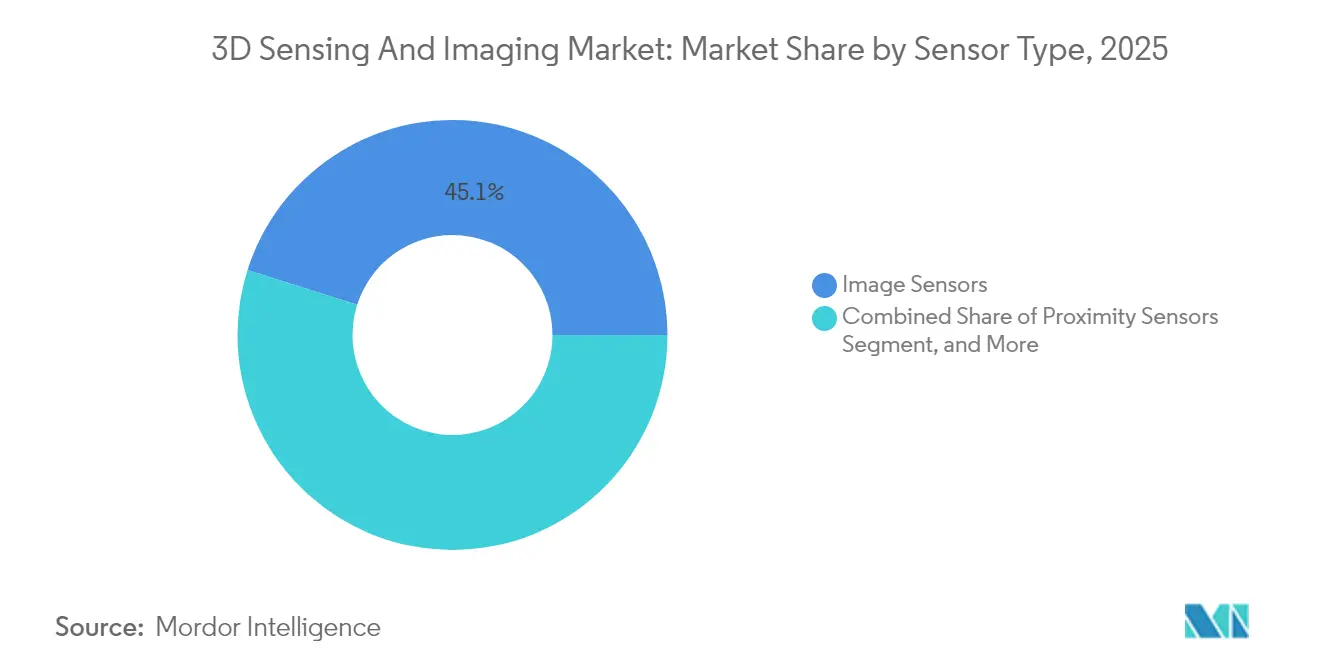
Image sensors accounted for 45.12% revenue in 2025, yet proximity sensors will grow 16.02% CAGR, buoyed by touchless interfaces in vehicles and operating rooms. 3D sensing-enabled human-machine interactions rely on short-range ToF or ultrasonic proximity data to wake displays, open doors, or trigger sterile-field commands. Multi-axis accelerometers and gyros embed motion cues that correct for hand jitter in mobile 3D scanning, widening adoption in construction and heritage preservation.
By Connectivity: Wireless Dominance Reflects Mobility Demands
Wireless links captured a 58.05% share in 2025 and will maintain a 14.71% CAGR as 5G release 17 introduces sidelink features ideal for vehicle-to-cloud depth-map uploads. Edge inference reduces bandwidth usage by 80%, transmitting only semantic scene graphs to enterprise servers. Wired Ethernet still rules inside factory cells and avionics cabins where latency determinism and electromagnetic immunity are paramount, prompting hybrid backbones that marry fiber spines with Wi-Fi 7 endpoints.
By End-User Industry: Healthcare Growth Challenges Consumer Electronics Leadership
Consumer electronics contributed 39.65% revenue in 2025 via smartphones, AR headsets, and gaming peripherals. The healthcare segment, expanding 16.08% CAGR, appropriates consumer sensor breakthroughs to power laparoscopic vision, dental scanning, and smart prosthetics. Surgical-robot OEMs demand sub-millimeter 3D accuracy, stimulating partnerships between optical sensor houses and medical-software vendors that navigate FDA 510(k) pathways.
Geography Analysis
North America led with 37.85% revenue in 2025, owing to entrenched automotive and medical-device manufacturers, yet Asia-Pacific is climbing 15.74% CAGR. Chinese handset and contract-manufacturing giants compress bill-of-materials to democratize depth cameras, while Japanese precision-machinery firms elevate quality inspection standards that require micron-level 3D capture. Korean display producers deploy in-line 3D profilometers to validate next-gen OLED stacks. India pilots satellite-based 3D soil-moisture mapping to optimize crop yields, signaling broader smart-agriculture uptake. Europe remains steady, driven by Euro NCAP mandates and industrial automation subsidies that reward machine vision investments.


Regulatory Landscape
Compliance is shaped by laser safety, EMC, automotive safety assessment, and emerging data and interoperability standards that affect how 3D point clouds and depth maps are generated, transmitted, and used. Across consumer and automotive deployments, laser products used in ToF modules and LiDAR systems are anchored to IEC 60825-1 requirements, while electronics also have to meet EMC regimes such as FCC Part 15 in the United States and the EMC Directive 2014/30/EU in Europe. These requirements influence module design, shielding, and validation cycles.
Standardization activity is expanding into both industrial and healthcare-adjacent use cases. In January 2026, the United States issued an RFI on diagnostic imaging interoperability standards and certification, reinforcing focus on standardized data exchange and certification pathways for imaging systems. In June 2026, NIST OSAC published an open-comment version of its Standard for Terrestrial LiDAR Scanner Data Capture (2025-N-0022) for forensic documentation workflows. At the same time, IEC TR 63145-400-20:2026 provided technical guidance for 3D sensing functions in eyewear displays, supporting more uniform integration practices for AR/VR form factors.
Value Chain Analysis
The 3D sensing and imaging value chain starts with upstream materials and device fabrication, including GaAs epi-wafers for VCSEL emitters, silicon wafers for CMOS image sensors, and specialty optics. It then moves into component manufacturing, covering lasers/VCSELs, photodiodes, ASICs/SoCs, and lenses and filters. Module integration follows, including optical alignment, calibration, packaging, and thermal design, before system-level OEMs in smartphones, vehicles, industrial automation, and medical devices deploy these components with software stacks for perception, calibration maintenance, and analytics.
Bottlenecks remain in precision optical packaging and alignment and in automotive-grade validation. Requirements tied to VDA 6.3 processes and AEC-Q102 qualification for optoelectronics extend lead times and raise entry barriers for new suppliers. Recent ecosystem moves also show how capacity and integration are being secured across foundry, sensor, and platform layers. In May 2026, Sony Semiconductor Solutions and TSMC signed an MoU to establish a joint venture for next-generation image sensor development and manufacturing in Kumamoto, linking sensor roadmaps more closely to advanced manufacturing access. On the platform side, Aeva integrated its 4D LiDAR as a reference sensor within NVIDIA DRIVE Hyperion (announced January 2026), and Nikon began commercial deployment of its APDIS MV5X laser radar system powered by Aeva (April 2026). Ouster and FUJIFILM also announced a May 2026 collaboration to embed organic color filter technology into digital lidar, indicating a push toward deeper materials and optics integration at the sensor level to improve data quality without relying solely on post-processing.
Competitive Landscape
Market fragmentation is moderate: legacy image-sensor titans Sony, STMicroelectronics, and Onsemi coexist with pure-play depth pioneers such as Aeva, Lumentum, and Airy3D. Semiconductor majors leverage wafer capacity and global sales channels, while startups differentiate with event-based neuromorphic arrays and quantum-dot short-wave-infrared hybrids. Keyence exploits vertical integration from optics through AI analytics, maintaining operating margins above 50%. Meanwhile, OmniVision’s April 2025 presence-detection sensor showcases single-die intelligence that sidesteps costly co-processors.[4]OmniVision Technologies, “OMNIVISION Announces New, Single Intelligent Sensor for Presence Detection, Facial Recognition and Always-On,” ovt.com Strategic directions favor mergers: Zebra bought Photoneo for logistics-automation depth cameras, and Viavi added Inertial Labs for position-aware test gear. Chipmakers pursue chiplet packaging to collapse lasers and photodiodes into CMOS interposers, aiming for sub-USD 1 bill-of-materials.
White-space opportunities span ultra-low-power IoT wake-on-motion modules and radiation-hardened lunar-surface mappers. Competitive advantage increasingly hinges on software ecosystems that transform raw point clouds into semantic maps, enabling vendors with machine-learning stacks to lock in customers through continuous model updates.
3D Sensing And Imaging Industry Leaders
Infineon Technologies AG
Microchip Technology Inc.
OmniVision Technologies Inc.
Qualcomm Inc.
Sick AG
- *Disclaimer: Major Players sorted in no particular order

Market Opportunities and Future Outlook
Edge-AI-native depth cameras and compact dToF modules are broadening deployment options in factories, logistics, and robotics, particularly where latency, bandwidth, and host compute constraints limit traditional RGB-D and point-cloud pipelines. RealSense used Automate 2026 to introduce the D585 Pro depth camera with on-camera edge AI and a Gen 5 SoC, and STMicroelectronics launched the VL53L9 compact direct ToF 3D LiDAR module with a 100 FPS frame rate. Together, these product launches reinforce a specific whitespace for vendors that bundle hardware with calibration, perception software, and lifecycle services, especially for high-mix industrial sites that need rapid commissioning and consistent updates.
Industrial interoperability and robotics scaling also create pull for 3D data standardization and higher unit throughput. IEEE published IEEE 2806-2025 for digital representation of physical objects in factory environments and approved IEEE 3141-2026 for 3D body processing, which can reduce integration friction across multi-vendor 3D datasets used in factory digital twins and human-centric applications. On the demand side, RoboSense reported 282,600 LiDAR units sold into robotics in H1 2026 with 510.4% year-over-year growth for that segment, supporting an active volume ramp for suppliers that can deliver robust calibration, cost-down, and manufacturing scale across modules and systems.
Recent Industry Developments
- June 2026: Qualcomm introduced the Snapdragon Reality Elite XR chipset and the START smart-glasses toolkit, pairing high on-device AI throughput with capabilities tuned for 3D environment reconstruction and camera passthrough. The combination of silicon plus turnkey reference designs reduces integration work for eyewear OEMs and can accelerate product cycles for spatial-computing devices that depend on depth-aware perception.
- July 2025: Zebra Technologies acquired Photoneo, adding 3D vision hardware and software used in logistics and industrial automation. The deal strengthens Zebra's ability to offer integrated warehouse automation stacks that combine scanning, perception, and workflows, increasing competitive pressure on standalone 3D camera suppliers.
- January 2024: Daimler Truck selected Aeva FMCW LiDAR for Level 4 trucking applications, signaling an OEM shift toward solid-state depth sensing with velocity measurement for long-haul autonomy. The win reinforced the role of automotive qualification and reliability as key gating factors, shaping supplier roadmaps around production-grade packaging and calibration stability.


Research Methodology Framework and Report Scope
Market Definition and Coverage
This market covers revenues generated from 3D sensing and imaging solutions that capture depth and build a 3D representation of objects or environments. The output is then used for measurement, recognition, navigation, and visualization across major end uses.
Scope exclusions: We exclude generic 2D imaging-only cameras and software that does not create or use depth data as a core output.
Segmentation Overview
- By Component
- Hardware
- Software
- Services
- By Technology
- Ultrasound
- Structured Light
- Time-of-Flight
- Stereoscopic Vision
- Other Technologies
- By Sensor Type
- Position Sensors
- Image Sensors
- Temperature Sensors
- Accelerometer Sensors
- Proximity Sensors
- Other Sensor Types
- By Connectivity
- Wired Network Connectivity
- Wireless Network Connectivity
- By End-user Industry
- Consumer Electronics
- Automotive
- Healthcare
- Aerospace and Defense
- Security and Surveillance
- Media and Entertainment
- Other End-user Industries
- By Geography
- North America
- United States
- Canada
- Mexico
- South America
- Brazil
- Argentina
- Chile
- Rest of South America
- Europe
- Germany
- United Kingdom
- France
- Italy
- Spain
- Rest of Europe
- Asia-Pacific
- China
- Japan
- South Korea
- India
- Singapore
- Australia
- Rest of Asia-Pacific
- Middle East and Africa
- Middle East
- Saudi Arabia
- United Arab Emirates
- Turkey
- Rest of Middle East
- Africa
- South Africa
- Nigeria
- Egypt
- Rest of Africa
- Middle East
- North America
Data Sources, Market Sizing, and Validation
Desk Research
Desk work starts by building the demand backdrop and the adoption triggers for depth-enabled devices and systems. We typically use public sources such as the US International Trade Commission for trade definitions, the OECD for digital and industry indicators, and standards references from ISO and IEC that clarify measurement and sensing terminology.
To keep assumptions grounded, we also review sources such as national statistical offices, US SEC filings and annual reports, customs and tariff schedules, and peer-reviewed journals focused on optics and computer vision. Patent databases are used to understand where R and D is concentrated and which modalities are being improved, and we reference an import and export shipment-level database selectively to sanity-check cross-border hardware flows. These desk sources are illustrative only, and we consulted additional public documents to collect data, validate inputs, and clarify open questions.
Primary Interviews and Surveys
Primary work focuses on checking what is actually shipping and being paid for, and how product mixes are changing by end use. We cover a spread of hardware makers, software and algorithm providers, system integrators, and downstream users in consumer electronics, automotive, industrial automation, healthcare, and security. Respondent coverage is balanced across APAC, EMEA, and the Americas to reduce single-region bias.
Distribution of primary research fieldwork respondents
| Company type | Respondent position | Region |
|---|---|---|
| Top tier: 39% | CXOs: 13% | APAC: 42% |
| Mid tier: 43% | Functional/Unit leaders: 27% | EMEA: 36% |
| Smaller Players: 18% | Managers: 60% | Americas: 22% |
Market-Sizing & Forecasting
The market model is first constructed using a top-down approach. We rebuild device and system demand pools using adoption rates for depth-enabled functions across key end uses, then convert those demand pools into value using typical price bands. After the demand pool is established, we corroborate the results with selective bottom-up approximations such as sampled ASP times estimated unit volumes for common module types, plus channel checks with integrators, and then adjust the output when the two views do not align.
Inputs are chosen to reflect how this market behaves in practice, so the model relies on indicators such as smartphone and consumer device shipment cycles, automotive feature penetration for driver monitoring and parking assist, industrial automation spending and machine vision uptake, medical imaging procedure and equipment refresh patterns, and the shift in technology mix between structured light, time-of-flight, stereo vision, and ultrasound. When data is missing for smaller countries or niche applications, we bridge gaps using proxy ratios from similar markets, and we test those bridges in interviews before finalizing them.
For forecasting, we mainly use scenario analysis supported by short time-series smoothing on the variables above, because demand can swing with consumer device launches and automotive regulation timing. The forward path is then reviewed with experts to confirm whether price erosion, integration levels, and attach rates are moving in the direction assumed.
Data Validation & Update Cycle
Validation is done by triangulating the model against independent signals such as regional shipment patterns, end-use spending direction, and observed technology mix changes. We compare those checks with the implied revenue outcomes. If a segment shows an unusual jump or drop, it is flagged for a second-pass review, and we re-contact a subset of respondents to confirm whether the change is real or driven by an input issue.
Before sign-off, we complete cross-checks across regional totals, growth rates, and pricing logic so the numbers add up in a consistent way across years. Reports are refreshed annually, and interim updates are completed when material events occur, followed by a final pre-delivery review so clients receive the most current view available.
Mordor Intelligence's 3d Sensing and Imaging Market Sizing Compared With Other Published Estimates
Published values for this market can look far apart because firms do not always count the same revenue streams, and they often use different timing for pricing and adoption. Some differences also come from whether an estimate assumes faster consumer electronics upgrades, or whether it weighs industrial and medical deployments that tend to move at a steadier pace.
The biggest gap driver is usually scope. Some figures fold in broader 3D imaging systems and mapping workflows, while others stay closer to depth-sensing modules and related software tied to recognition and measurement use cases. Currency timing and the way price erosion is applied across structured light and time-of-flight can also move totals, and so can refresh cadence when a major device cycle changes in-year. This is why the defined component split and yearly input refresh were kept explicit in our model, a choice applied by Mordor Intelligence.
Benchmark comparison
| Source | Market Size | Gaps in Research Methodology |
|---|---|---|
| Mordor Intelligence | USD 13.16 B (2025) | |
| Industry Research House A | USD 39.00 B (2025) | Uses a broader definition that appears to include more full-system 3D imaging platforms and adjacent scanning and mapping workflows, which expands the counted revenue base beyond core depth-enabled sensing and imaging functions. |
| Industry Publisher B | USD 19.00 B (2025) | Leans on a higher near-term adoption and pricing assumption for consumer-facing devices, with less transparency on technology-mix pricing and currency timing, which can inflate the first forecast year versus a component- and modality-checked build. |
Taken together, the spread is mostly explained by what gets counted and how quickly pricing and adoption are assumed to move in the early years. By tying the estimate to observable demand pools, clear technology mix assumptions, and repeatable pricing logic, we keep the outcome traceable and easier to reconcile against real shipment and deployment signals over time.


Key Questions Answered in the Report
How large is the global 3D sensing and imaging market in 2026?
The market is valued at USD 14.98 billion in 2026.
What compound annual growth rate is projected through 2031?
A 13.84% CAGR is forecast between 2026 and 2031.
Which component category is expanding fastest?
Services are growing at 14.88% CAGR, reflecting demand for turnkey depth-sensing solutions.
Which technology segment leads today?
Time-of-flight holds 43.25% of 2025 revenue and remains the largest technology segment.
Which region is expected to grow most rapidly?
Asia-Pacific is advancing at a 15.74% CAGR, driven by manufacturing scale and smartphone production.
What is restraining near-term supply?
Limited gallium arsenide epi-wafer capacity is delaying VCSEL production and raising component costs.
Page last updated on: