
3D IC Packaging Market Size and Share
Market Overview
| Study Period | 2020 - 2031 |
|---|---|
| Market Size (2026) | USD 18.64 Billion |
| Market Size (2031) | USD 37.41 Billion |
| Growth Rate (2026 - 2031) | 14.95 % |
| Fastest Growing Market | Middle East and Africa |
| Largest Market | Asia Pacific |
| Market Concentration | Low |
Major Players
*Disclaimer: Major Players sorted in no particular order Image © Mordor Intelligence. Reuse requires attribution under CC BY 4.0. |
|
3D IC Packaging Market Analysis by Mordor Intelligence
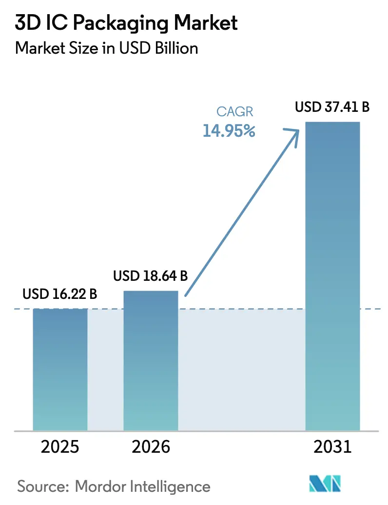
3D IC packaging market size in 2026 is estimated at USD 18.64 billion, growing from 2025 value of USD 16.22 billion with 2031 projections showing USD 37.41 billion, growing at 14.95% CAGR over 2026-2031. This surge is propelled by soaring artificial-intelligence and high-performance-computing workloads that outstrip the bandwidth, latency and power limits of conventional 2D layouts, forcing semiconductor vendors to adopt vertically stacked architectures. Advanced memory such as HBM4+ and logic-to-memory co-design inside the 3D IC packaging market are resetting cost hierarchies, while supply–demand imbalances in through-silicon-via (TSV) tooling and CoWoS substrates temper near-term output expansion. Asia-Pacific maintains a formidable lead thanks to Taiwan and South Korea’s tightly integrated foundry clusters, but North American reshoring under the CHIPS Act and Gulf-region green-field programs are altering long-term capacity maps. Intensifying export-control regimes, coupled with defense-grade security mandates, compel foundries to re-engineer equipment procurement and partner networks without compromising time-to-yield.[1]
Key Report Takeaways
- By packaging technology, 3D TSV retained 37.96% of the 3D IC packaging market share in 2025, while hybrid-bond stacking is projected to compound at 21.15% CAGR through 2031.
- By integration approach, 2.5D interposers held 57.38% share of the 3D IC packaging market in 2025; true 3D stacking shows the steepest growth at 21.28% CAGR to 2031.
- By device type, memory—dominated by HBM stacks—accounted for 40.35% of the 3D IC packaging market size in 2025; HBM4+ volumes are poised for a 23.86% CAGR through 2031.
- By end-user application, HPC and AI captured 37.45% revenue share of the 3D IC packaging market in 2025 and is on track for a 19.05% CAGR to 2031.
- By geography, Asia-Pacific led with 62.41% share in 2025, whereas the Middle East and Africa region is forecast to register a 19.06% CAGR between 2026 and 2031.
Note: Market size and forecast figures in this report are generated using Mordor Intelligence’s proprietary estimation framework, updated with the latest available data and insights as of 2026.
Global 3D IC Packaging Market Trends and Insights
Drivers Impact Analysis*
| Driver | (~) % Impact on CAGR Forecast | Geographic Relevance | Impact Timeline |
|---|---|---|---|
| Explosive AI / HPC demand for HBM-stacked packages | 4.20% | Global, concentrated in North America & APAC | Short term (≤ 2 years) |
| Mobile & wearables shift to Wafer-Level Chip-Scale Packages (WLCSP) | 2.80% | APAC core, spill-over to North America | Medium term (2-4 years) |
| Foundry "Foundry 2.0" strategy integrating packaging | 2.10% | Global, led by Taiwan & South Korea | Medium term (2-4 years) |
| Glass-core & panel-level substrates lowering cost at scale | 1.90% | APAC manufacturing, global deployment | Long term (≥ 4 years) |
| Defense-grade chiplets mandate secure heterogeneous integration | 1.40% | North America & EU, selective APAC | Long term (≥ 4 years) |
| Carbon-neutral fabs prioritising low-temperature hybrid bonding | 0.80% | EU & North America, expanding to APAC | Long term (≥ 4 years) |
| Source: Mordor Intelligence | |||
Explosive AI / HPC Demand for HBM-Stacked Packages
A wave of data-center accelerators is reshaping bill-of-materials priorities, pushing HBM stacks inside the 3D IC packaging market to the top of every advanced-node roadmap. TSMC is scaling CoWoS output to 88,000 wafers per month by 2026 to keep pace with Nvidia’s next-generation GPUs. The shift from HBM3E to HBM4+ triples effective bandwidth density while holding thermal design limits steady, forcing substrate makers to qualify thicker core materials and finer copper redistribution layers. Samsung’s H-Cube platform couples’ logic and memory on-package, illustrating how memory-centric topologies are cascading down to board-level architecture. The net effect is a higher stacked-die ratio per device, a richer TSV mix and, ultimately, an elevated ASP across the 3D IC packaging market.
Mobile and Wearables Shift to Wafer-Level Chip-Scale Packages (WLCSP)
Wearable and premium-smartphone OEMs now view wafer-level system-in-package footprints as the default path to squeezing radios, PMICs and MEMS into sub-7 mm platforms. Apple’s 2026 flagship is widely expected to showcase advanced WLCSP for its A-series SoC, a signal that form-factor is trumping traditional cost-per-pin trade-offs. Taiwanese OSATs have responded by doubling lithography lines dedicated to redistributed-layer-count (RDL)-first flows, while South Korean rivals pivot toward resin-coated copper foils to mitigate warpage. These moves expand the 3D IC packaging market beyond data-center silicon and into everyday consumer devices, diversifying revenue streams and improving fab loading factors.
Foundry “Foundry 2.0” Strategy Integrating Packaging
The boundary between wafer fabrication and advanced packaging vanished once node-to-node transistor gains slipped below historical norms. TSMC’s USD 65 billion Arizona campus now dedicates two buildings exclusively to CoWoS and SoIC services. Samsung’s roadmap marries 2 nm FEOL with 2.5D H-CUBE back-end in the same cleanroom complex, lowering inter-factory cycle time by 30%. Intel Foundry Services, meanwhile, bundles Foveros Direct and EMIB with reticle-stitching options, allowing customers to marry leading-edge compute tiles with mature I/O dice. Vertical integration lifts margin accelerates yield learning and positions foundries as one-stop shops for the full 3D IC packaging market lifecycle.[2]
Glass-Core and Panel-Level Substrates Lowering Cost at Scale
Organic substrates cannot meet the co-planarity and CTE requirements of ≥50 Gbps die-to-die links, prompting early adoption of glass-core laminates that support through-glass vias (TGVs). Intel’s 2025 pilot showed a 40% reduction in skew variance across 300 mm glass cores, paving the way for panel-level stitching onto 510 mm × 515 mm substrates. TSMC’s panel-level packaging program targets a 20–30% unit-cost drop for AI accelerators by 2027, while C Sun and Mycronic ship over-size lithography gear to Taiwan OSATs. As economies of scale kick in, glass-based carriers will widen the addressable tier-2 customer base of the 3D IC packaging market.
Defense-Grade Chiplets Mandate Secure Heterogeneous Integration
U.S. and European defense agencies now specify tamper-resistant, multi-vendor chiplet stacks that can be audited down to individual bump geometry. Programs such as the U.S. SHIP initiative fund prototype runs where logic processed at a trusted North American fab is hybrid-bonded to Asia-Pacific-sourced RF dice within secure facilities. The requirement for onshore trusted flows, secure firmware provisioning and lifetime traceability raises the engineering content per unit and injects premium pricing into specialized corridors of the 3D IC packaging market. Supply-chain transparency tools and cryptographic die-to-die links are becoming as critical as mechanical alignment accuracy.
Restraints Impact Analysis*
| Restraint | (~) % Impact on CAGR Forecast | Geographic Relevance | Impact Timeline |
|---|---|---|---|
| Scarcity of production TSV tools and CoWoS capacity | -3.10% | Global, most severe in APAC | Short term (≤ 2 years) |
| Thermal-design-limit (TDL) challenges beyond 1 W/mm² | -2.40% | Global, critical for HPC applications | Medium term (2-4 years) |
| High IP / EDA cost for 3D floor-planning | -1.80% | Global, concentrated in design centers | Medium term (2-4 years) |
| Panel warp and yield loss >3% in early PLP lines | -1.20% | APAC manufacturing hubs | Short term (≤ 2 years) |
| Source: Mordor Intelligence | |||
Scarcity of Production TSV Tools and CoWoS Capacity
TSV etchers, bonding aligners and CoWoS-grade substrate laminators remain booked 12–18 months out, constraining upside for OSATs scrambling to meet AI accelerator schedules. Applied Materials and Tokyo Electron both forecast double-digit equipment backlog into mid-2026, yet component shortages and install-crew bottlenecks slow actual ramp-ups. With TSMC commanding the lion’s share of CoWoS substrates, buyers compete for wafer-start allocations, sometimes pre-paying quarters in advance. The scarcity curtails immediate revenue realization across the 3D IC packaging market even when demand signals are unmistakably strong.[3]
Thermal-Design-Limit (TDL) Challenges Beyond 1 W/mm²
As stacked dies exceed 1 W/mm², conventional heat-spreaders fail to evacuate junction heat in the middle tiers. TSMC is piloting microfluidic cooling channels etched directly into silicon interposers, but early-stage prototypes add manufacturing complexity and uncertain reliability. Device builders must therefore throttle clocks or adopt spread-out chiplet layouts, diluting some performance gains and nudging power budgets upward. The gap between cooling innovation and power-density escalation will persist throughout the decade, shaving points off the compound trajectory of the 3D IC packaging market.
*Our forecasts treat driver/restraint impacts as directional, not additive. The impact forecasts reflect baseline growth, mix effects, and variable interactions.
Segment Analysis
By Packaging Technology: TSV Leadership Faces Hybrid Bonding Disruption
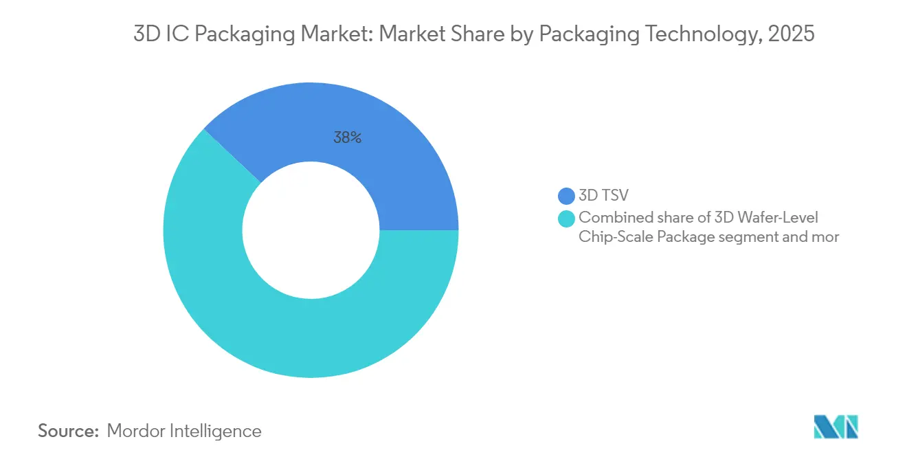
3D TSV nodes retained 37.96% of the 3D IC packaging market share in 2025 because mature lithographic rules, bulk production tooling and field reliability data aligned with memory vendors’ cost-per-GB targets. Multiple HBM3E lines already amortized their TSV drill and fill equipment, stabilizing gross margins even as die counts increased. Yet the hybrid-bond segment is expanding at a 21.15% CAGR, levering copper-to-copper direct contact to cut z-height by 40% and interconnect resistance by 15%. These electrical gains are pivotal in compute-dense AI accelerators that push beyond traditional package-substrate escape routing limits.
The pivot does not render TSV obsolete. Instead, dual-path roadmaps emerge: TSV remains the default for high-volume memory and sensor stacks, while hybrid bonding occupies compute-centric, low-latency corners of the 3D IC packaging market. OSATs able to host both flows on adjacent lines secure risk-diversified bookings. As substrate makers scale glass cores, hybrid bonding alignment accuracy improves further, hinting at future cross-over where cost curves intersect and hybrid bonding usurps TSV in certain volume SKUs.

By Integration Approach: Interposer Dominance Challenged by True 3D Evolution
2.5D interposers booked 57.38% revenue in 2025, capitalizing on a decade of yield learning that brought silicon-interposer defectivity to <0.1 dpm. Because interposers decouple front-end node choice from back-end assembly, GPU vendors ship reticle-sized compute tiles beside older-node I/O dies without redesigning the full stack. However, true 3D stacking logs a 21.28% CAGR, fuelled by die-to-die latency gains that can cut model-training time by double-digit percentages. Flagship use cases include vertical NAND, near-memory compute lenses and in-package high-Q RF filters—all scenarios where z-axis proximity beats planar reticulation.
Early reliability fears—electro-migration in buried micro-bumps and thermo-mechanical shear at die corners—are being mitigated by low-modulus under-fills and hybrid-bond copper diffusion barriers. As micro-fluidic cooling and graphene heat-spreaders mature, true 3D adoption accelerates. The 3D IC packaging market therefore bifurcates into an interposer mainstream and a true-stacked performance edge, each advancing on differentiated KPI roadmaps rather than price alone.
By Device Type: Memory Applications Drive HBM4+ Innovation
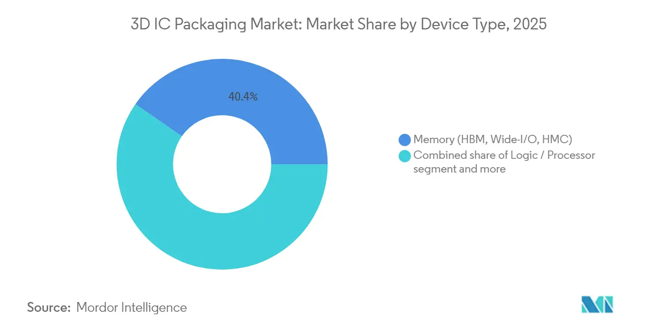
Memory held 40.35% of 2025 revenue, the single largest usage slice inside the 3D IC packaging market. The impending jump to HBM4+—slated for high-volume ramp in 2027—injects a forecast 23.86% CAGR for memory-centric packages through 2031. Stacked-memory vendors co-design channel architecture and micro-bump pitch with foundry partners to preserve signal integrity at >1 Tbps aggregate bandwidth. Logic-plus-memory cobonds yield SKU-specific trade-offs: more layers raise cache residency but translate into tougher thermal budgets.
Outside memory, logic processors gain share through chiplet partitioning that mixes EUV-patterned compute tiles with mature-node PHY dice. Sensor and MEMS modules adopt 3D WLCSP to marry optical, inertial and environmental sensing within dental-paste-sized packages for wearables and automotive cabins. RF and analog players harness vertical isolation inside glass cores to shield noise-sensitive blocks even as 5G FR2 frequencies cross 52 GHz. Each device sub-niche shapes its own cost-performance envelope within the 3D IC packaging market, driving demand diversity and smoothing capacity utilization.
By End-User Application: HPC and AI Dominance Reshapes Industry Priorities
HPC and AI workloads seized 37.45% of 2025 sales and are projected to rise at a 19.05% CAGR through 2031, catapulting accelerator vendors to the top tier of package-substrate allocation. Cloud hyperscalers increasingly sidestep merchant silicon and fund custom ASICs stitched inside CoWoS or panel-level carriers, ensuring guaranteed slotting in the 3D IC packaging market. With model-parameter counts doubling every nine months, bandwidth per millimetre of substrate outpaces Moore-era transistor density as the key metric.
Consumer electronics retains scale momentum—especially as OEMs add mixed-reality compute to smartphones—but its pricing power pales next to data-center ASPs. Automotive and ADAS designs, governed by AEC-Q100 and ISO 26262, seek extended runtimes over a −40 °C-to-150 °C envelope, nudging suppliers to adopt under-fill chemistries resistant to temperature cycling. Aerospace and defence embrace secure chiplets and radiation-hard dielectrics, paying 3–5 × consumer ASP per square millimetre. Medical and Industrial IoT packages prioritise photonic sensors and extreme-low-leakage logic, broadening the footprint of the 3D IC packaging market without diluting its technology edge.
Geography Analysis
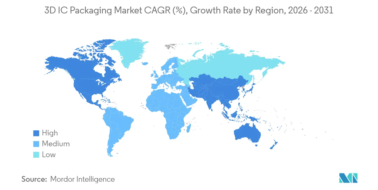
Asia-Pacific commanded 62.41% of the 3D IC packaging market in 2025, a consequence of Taiwan’s advanced-node hegemony, South Korea’s memory-centric back-end clusters and mainland China’s sprint toward domestic capacity. TSMC’s CoWoS, Samsung’s H-Cube and ASE’s FOCoS platforms anchor dense supplier habitats, driving low logistics latency and fast process transfer loops. Even so, relocation risk under geopolitical crosscurrents pushes some customers to dual source into Malaysia, Singapore and Vietnam, lengthening the region’s technology reach while marginally raising cost baselines.
North America benefits from USD-denominated CHIPS Act incentives that subsidize capex for both leading-edge wafers and advanced packaging lines. TSMC Arizona and Intel Ohio collectively exceed a projected 100,000 wafers per month of back-end capacity by 2028, a cushion against Asia-bound supply disruption. Proximity to Nvidia, AMD and a host of machine-learning start-ups tightens design-manufacturing feedback loops, granting North America disproportionate influence over the direction of the 3D IC packaging market even if absolute volume lags Asia.
The Middle East and Africa region posts the highest forecast CAGR at 19.06%, albeit from a small base. Sovereign-wealth-fund-backed fabs in the UAE and Saudi Arabia’s Vision 2030 industrial zones earmark billions for glass-core substrate lines and OSAT pilot plants. Europe focuses on automotive reliability and green-manufacturing leadership, leveraging German power-electronic expertise and French photonics clusters. Latin America remains a niche assembly point for consumer devices, while Eastern Europe eyes defense-oriented secure-package initiatives. Together, these moves fragment capacity geographically, opening localized demand pockets inside the broader 3D IC packaging market.
Regulatory Landscape
Policy support and trade controls are shaping both where 2.5D/3D packaging capacity is built and which toolchains can be deployed. In the United States, the CHIPS and Science Act framework includes USD 11 billion in R&D funding, and NIST-led programs such as the National Advanced Packaging Manufacturing Program (NAPMP) emphasize advanced packaging, metrology, and prototyping as strategic capabilities for onshore scaling.
Cross-border shipment of advanced packaging equipment and AI-class devices faces tighter scrutiny. In 2026, U.S. Bureau of Industry and Security (BIS) updates expanded licensing requirements that include packaging-relevant tools and high-bandwidth memory stacks, pushing OSATs and foundries to strengthen export classification and end-use due diligence. In Europe, the European Commission proposed a new Chips Act package in 2026 that includes support for first-of-a-kind facilities combining leading-edge manufacturing with 2.5D/3D chiplet integration, reinforcing the role of public-private programs in de-risking advanced packaging investments.
Value Chain Analysis
The 3D IC packaging value chain starts with upstream materials and equipment, then concentrates in wafer fabs and OSATs that execute TSV formation, bonding (including hybrid bonding and thermocompression), advanced substrates/interposers, and final test. Critical upstream inputs include ABF-based substrate materials, high-precision bonding and alignment systems, TSV etch/fill toolsets, metrology/inspection, and advanced test infrastructure for large heterogeneous packages. Midstream activity is anchored by foundry-integrated packaging offerings (for example CoWoS and SoIC) alongside OSAT platforms, while downstream demand is pulled by HPC and AI accelerators that draw in HBM stacks and high-layer-count substrates.
Capacity and substrate bottlenecks are most visible in CoWoS-grade assembly, which raises the importance of coordination among foundries, OSATs, and substrate suppliers. TSMC expanded its 3DFabric Alliance in 2026 to include additional substrate and materials partners, and alliance participation also broadened to research-oriented contributors such as imec. This supply-chain posture links design enablement, process modules, and qualified materials. Geographic diversification is also showing up through announced or advancing US-based advanced packaging footprints (including Arizona-linked initiatives) alongside Asia-based expansions, reducing single-site dependency but increasing the complexity of qualification, logistics, and export-compliance management.
Competitive Landscape
Technological differentiation rather than labour cost now dictates competitive rank. TSMC and Samsung together hold the premium slice of the 3D IC packaging market with CoWoS, SoIC and H-Cube portfolios addressing compute and memory concurrently. ASE Group retains volume leadership in versatile FOCoS flows, while Amkor champions turnkey service for consumer SOCs. Intel Foundry Services bridges FEOL and BEOL with Foveros Direct plus EMIB, luring fabless clients seeking node-agnostic chiplet aggregation.
Chinese contenders—JCET, Huahong and SMIC’s packaging arms—narrow process gaps by licensing hybrid-bond aligners and TSV etchers, accelerating domestic uptake under the national “advanced packaging first” policy. Equipment access constraints and export-licence uncertainty, however, complicate scale-up pace. Japanese specialists such as Ibiden and Shinko Electric secure high-TG BT substrates and next-gen Ajinomoto-build-up films, undergirding the material backbone of the 3D IC packaging market. Patent thickets in copper direct bonding and elastomer-embedded micro-fluidics grant early entrants’ defensible moats, but standards bodies—chiefly the UCIe Consortium—chip away at proprietary interposer and chiplet link protocols, gradually commoditizing baseline connectivity.
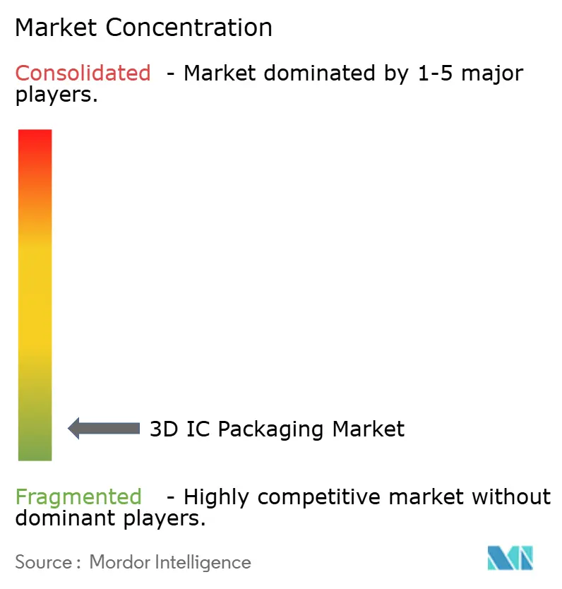
Strategic moves over the past 18 months underline a pivot toward end-to-end verticals. TSMC’s USD 35 billion multiyear capex uplift channels one-third of spend into BEOL packaging, while Samsung corrals logic, DRAM and packaging into a single business unit. ASE’s Penang mega-campus triples cleanroom footage, signalling OSAT commitment to HPC packages. In response, equipment vendors consolidate through M and A—e.g., Lam Research’s acquisition of a specialist panel-warpage metrology start-up—to anchor share in a swelling capex cycle. Competition is therefore dynamic but not yet fragmented, keeping the 3D IC packaging market moderately concentrated.[4]
3D IC Packaging Industry Leaders
-
Taiwan Semiconductor Manufacturing Company Limited
-
Advanced Semiconductor Engineering Inc.
-
Amkor Technology Inc.
-
Samsung Electronics Co., Ltd.
-
Siliconware Precision Industries Co. Ltd.
- *Disclaimer: Major Players sorted in no particular order
Market Opportunities and Future Outlook
One clear whitespace is at the intersection of capacity, test, and yield-learning for large AI/HPC packages, where incremental wafer-fab output does not translate into shipped systems without commensurate CoWoS-class assembly and advanced testing. Investment and build activity in major hubs support this view: ASE Technology Holding began construction in April 2026 on a new advanced semiconductor testing facility in Kaohsiung (Renwu Industrial Park), and SK hynix announced a large-scale advanced packaging facility plan in Cheongju with a defined construction and completion timeline through 2027-2028. These moves point to an expanding spend envelope across bonding and interconnect, plus high-throughput test, burn-in, and reliability screening that determines end-customer shipments.
Technology roadmaps also create opportunities in finer-pitch heterogeneous integration and in new substrate formats that reduce cost per I/O while supporting larger reticle-scale assemblies. TSMC has publicly outlined a SoIC scaling path toward 4.5 micrometer interconnect pitch by 2029, reinforcing hybrid bonding as a key enabler for higher I/O density and lower parasitics in true 3D stacks. At the same time, panel-format concepts (for example chip-on-panel approaches) and glass-related interposer development efforts broaden the pathway for suppliers of oversize lithography, metrology, warpage control, and advanced substrate materials, particularly where ABF and interposer supply constraints limit package throughput.
Recent Industry Developments
- July 2026: Taiwan officials disclosed plans for TSMC to add advanced packaging plants in Chiayi Science Park as part of a new phase of expansion. The program underscores how CoWoS-class packaging has become a primary constraint for AI accelerators, and it signals further clustering of packaging capacity alongside Taiwan’s existing advanced-node ecosystem.
- June 2026: TSMC and Amkor Technology announced a long-term partnership focused on advanced packaging and testing in Arizona. The agreement supports a more geographically distributed back-end supply chain for 2.5D/3D packages and improves alignment between foundry wafer output and downstream packaging/test availability in the United States.
- June 2025: Broadcom introduced its 3.5D eXtreme Dimension System in Package, integrating a very large silicon footprint with multiple HBM stacks. The launch illustrates continuing escalation in package size and memory integration, increasing demand for high-yield interconnect, substrate capability, and advanced thermal and test solutions.
Research Methodology Framework and Report Scope
Market Definition and Coverage
For this study, the 3D IC packaging market covers revenue generated from packaging solutions that stack multiple dies in a single package to improve bandwidth, reduce footprint, and shorten interconnect lengths across electronic systems.
Scope exclusions: This sizing does not count traditional 2D packages and general outsourced assembly revenue that is not tied to 3D stacking architectures.
Segmentation Overview
-
By Packaging Technology
- 3D TSV
- 3D Wafer-Level Chip-Scale Package (WLCSP)
- Hybrid-Bond Stacking (WoW, CoW, SoIC)
- Fan-Out 3D & Panel-Level Packaging (PLP)
-
By Integration Approach
- 2.5D Interposer
- True 3D Stacking
- System-in-Package / Chiplet-based HI
-
By Device Type
- Memory (HBM, Wide-I/O, HMC)
- Logic / Processor
- Sensor & MEMS
- RF & Analog
-
By End-User Application
- High-Performance Computing & AI
- Consumer Electronics & Mobile
- Automotive & ADAS
- Aerospace & Defence
- Medical & Industrial IoT
-
Geography
-
North America
- United States
- Canada
- Mexico
-
Europe
- United Kingdom
- Germany
- France
- Italy
- Rest of Europe
-
Asia-Pacific
- China
- Japan
- India
- South Korea
- Rest of Asia
-
Middle East
- Israel
- Saudi Arabia
- United Arab Emirates
- Turkey
- Rest of Middle East
-
Africa
- South Africa
- Egypt
- Rest of Africa
-
South America
- Brazil
- Argentina
- Rest of South America
-
North America
Data Sources, Market Sizing, and Validation
Desk Research
Desk research was used to set the boundaries of what qualifies as 3D IC packaging and to anchor the model to real industry signals. We relied on public, non-paywalled sources such as USITC trade data, the OECD STAN database, SEMI updates, IEEE publications, and ITRS style roadmaps and technical proceedings, since these sources help show where packaging technology is heading and what demand is pulling it forward.
We also reviewed company annual reports, investor presentations, and earnings transcripts to understand capacity expansion timing, advanced packaging investment plans, and end-market exposure. Where needed, we cross-checked key figures using paid subscriptions for company financials and news intelligence, patent databases for activity trends, and an import and export shipment-level database to sanity-check equipment and materials flow. These desk sources are not exhaustive, and we used additional public references for data collection, validation, and clarification during the research.
Primary Interviews and Surveys
Primary work helped convert technical adoption stories into measurable assumptions that could be modeled, then validated with people who see orders and volumes. We spoke with stakeholders across OSAT and packaging ecosystem functions, device supply chain leaders, and end-user engineering and sourcing teams across major geographies, so gaps from desk research could be filled and checked again before finalizing the sizing.
Distribution of primary research fieldwork respondents
| Company type | Respondent position | Region |
|---|---|---|
| Top tier: 36% | CXOs: 14% | APAC: 53% |
| Mid tier: 49% | Functional/Unit leaders: 42% | EMEA: 29% |
| Smaller Players: 15% | Managers: 44% | Americas: 18% |
Market-Sizing & Forecasting
Sizing starts from a top-down build where semiconductor packaging demand is reconstructed using adoption rates of 3D stacking by end-user use cases, and then filtered through packaging technology mix before it is converted into USD value. We corroborated the totals with selective bottom-up checks, such as sampled price per package ranges times estimated unit volumes for key device categories, plus a few supplier roll-ups where public disclosures supported those views.
Inputs used in the model include, for example, advanced node wafer starts that drive higher-density packaging needs, HBM attachment and stacking trends for AI and HPC, the share shift between 3D TSV and 3D WLCSP formats, OSAT and foundry advanced packaging capacity additions, and cycle timing in consumer electronics and automotive programs. When a bottom-up check showed gaps, we used conservative proxy ranges and then re-tested them in interviews, so the final number did not hinge on a single hard-to-obtain data point.
For forecasting, scenario analysis was used because this market is strongly affected by capacity ramp timing and end-market demand swings. A base case is created from consensus primary inputs on adoption speed and pricing progression, followed by upside and downside cases around yield learning, capex execution, and product cycle timing. The midpoint of these cases is used for the published forecast.
Data Validation & Update Cycle
Results are triangulated across independent checks, where model outputs are compared with related signals such as packaging capacity announcements, shipment proxies from trade series, and the observed pace of AI and HPC deployments. Large variances are investigated by drilling into the specific assumption that drove the difference, and then re-contact is triggered when a key input like capacity timing or pricing moves outside the expected range.
Before sign-off, the work goes through multi-step analyst reviews to confirm that units, currency conversion timing, and year mapping are consistent across all tables and charts. The report is refreshed annually, and interim updates are made when material events occur, including major capacity expansions, sudden demand shocks, or policy changes affecting supply chains. Right before delivery, a final review pass is completed so clients receive the latest updated view.
Mordor Intelligence's 3d Ic Packaging Market Estimate Compared With Other Published Estimates
Published market sizes for 3D IC packaging can look far apart because authors do not always count the same revenue pool, and the timing of the base year also changes what gets captured. The benchmark table makes this spread easy to see, and it highlights differences that often come from scope boundaries, pricing paths, and how quickly assumptions are updated.
The table shows a meaningful gap versus sources that bundle nearby categories together, and in Mordor Intelligence's model, only 3D IC packaging revenue tied to die stacking architectures is counted, rather than folding in broader advanced packaging or 2.5D interposer value by default. Another driver is how price and mix are handled, since some estimates apply one blended ASP across technologies, while our approach models separate mix shifts for 3D TSV and 3D WLCSP and then checks them with primary feedback. Currency timing and refresh cadence also matter, because using a different conversion window or not revisiting capacity ramp assumptions after major expansion news can move the market value up or down.
Benchmark comparison
| Source | Market Size | Gaps in Research Methodology |
|---|---|---|
| Mordor Intelligence | USD 18.64 B (2026) | |
| Trade Journal A | USD 18.35 B (2025) | Uses a nearby year and often groups 3D packaging with a wider 3D semiconductor packaging bucket, which can mix in formats that are not strictly die-stacked IC packages, and it may apply a broad blended pricing curve. |
| Industry Research Portal B | USD 6.34 B (2025) | Combines 2.5D and 3D in the title but appears to size a narrower captured revenue base, which can undercount high-value AI and HPC packaging, and it uses a longer forecast horizon that smooths near-term ramp effects. |
Taken together, the differences mostly come from what is included, which year is used as the anchor, and whether technology mix is explicitly modeled. By tying the value build-up to observable demand signals and then cross-checking key assumptions with industry interviews, the estimate stays traceable to clear inputs and repeatable calculation steps.
Key Questions Answered in the Report
What is the current size of the 3D IC packaging market?
The 3D IC packaging market size reached USD 18.64 billion in 2026 and is forecast to hit USD 37.41 billion by 2031.
Which segment leads the 3D IC packaging market?
By technology, 3D TSV maintains leadership with 37.96% share, though hybrid-bonding is the fastest-growing segment.
Why is Asia-Pacific dominant in 3D IC packaging?
Asia-Pacific hosts the densest cluster of foundries and OSATs—chiefly in Taiwan and South Korea—giving it 62.41% market share in 2025.
How fast is the HPC and AI application segment growing?
HPC and AI packages are projected to expand at a 19.05% CAGR, reflecting rising demand for memory-centric accelerator designs.
What are the main restraints on market growth?
Capacity shortages in TSV and CoWoS tooling, thermal-design-limit challenges above 1 W/mm², and high 3D EDA licensing costs collectively dampen near-term expansion.
Which new technologies could lower advanced packaging costs?
Glass-core and panel-level substrates promise 20–30% unit-cost reductions once high-volume lines mature, reshaping future cost curves in the 3D IC packaging market.